1. General description - nxp.com · SDCD A16 I SD card detect (active LOW). This pin can be used to...
37
1. General description The SDIO101A is a SD/SDIO/MMC/CE-ATA host controller with a standard 16-bit asynchronous memory interface. The device conforms to the SD Host Standard Specification Version 2.0 (see Ref. 1 ). The SDIO101A manages the physical layer of SD, SDIO, MMC and CE-ATA protocols and can be used together with SD Host Standard compatible driver software to add SD/SDIO/MMC/CE-ATA host functionality to a variety of microprocessor systems. The SDIO101A supports both full-speed (< 25 MHz) and high-speed (< 52 MHz) data transmissions on the SD/SDIO/MMC/CE-ATA port. The SDIO101A offers separate pins for SD/SDIO/MMC/CE-ATA port supply voltage, host interface supply voltage and core supply voltage. The SD/SDIO/MMC/CE-ATA port can operate at a wide voltage range (1.8 V to 3.6 V) which allows the device to interface to a large variety of SD, SDIO, MMC or CE-ATA devices. The SDIO101A allows 1-bit and 4-bit SD transactions and 8-bit MMC/CE-ATA transactions. The 16-bit asynchronous memory interface can operate at a 2.5 V to 3.6 V voltage range. A built-in, 2 kB data buffer allows for a low interrupt latency time and efficient communication with the host processor at high data rates. The SDIO101A provides a DMA request line that can be connected to an external DMA controller to off-load the host processor and increase overall system performance. An on-board PLL allows a large range of SD/SDIO/MMC/CE-ATA clock speeds to be generated from a single externally available clock source. An additional fractional divider allows the SD clock speed to be fine-tuned with very fine granularity, which enables the user to achieve the maximum desired SD clock speed from the external clock source. The SDIO101A offers 5 levels of power saving, including a ‘Hibernate mode’ where the on-board oscillator, PLL and data buffer memories are switched off, and a ‘Coma mode’ in which supply power to most of the device is internally switched off. This allows the device to be used in very power-critical applications. 2. Features and benefits 2.1 General Provides 1 SD/SDIO/MMC/CE-ATA slot, operating in 1-bit, 4-bit and 8-bit (MMC/CE-ATA) modes 2.5 V to 3.3 V host interface 1.8 V core supply voltage Separate SD supply voltage pin. SD/SDIO/MMC/CE-ATA slot is able to operate at a wide voltage range (1.8 V to 3.3 V). SDIO101A SD/SDIO/MMC/CE-ATA host controller Rev. 1 — 13 June 2013 Product data sheet
Transcript of 1. General description - nxp.com · SDCD A16 I SD card detect (active LOW). This pin can be used to...

1. General description
The SDIO101A is a SD/SDIO/MMC/CE-ATA host controller with a standard 16-bit asynchronous memory interface. The device conforms to the SD Host Standard Specification Version 2.0 (see Ref. 1). The SDIO101A manages the physical layer of SD, SDIO, MMC and CE-ATA protocols and can be used together with SD Host Standard compatible driver software to add SD/SDIO/MMC/CE-ATA host functionality to a variety of microprocessor systems.
The SDIO101A supports both full-speed (< 25 MHz) and high-speed (< 52 MHz) data transmissions on the SD/SDIO/MMC/CE-ATA port. The SDIO101A offers separate pins for SD/SDIO/MMC/CE-ATA port supply voltage, host interface supply voltage and core supply voltage. The SD/SDIO/MMC/CE-ATA port can operate at a wide voltage range (1.8 V to 3.6 V) which allows the device to interface to a large variety of SD, SDIO, MMC or CE-ATA devices. The SDIO101A allows 1-bit and 4-bit SD transactions and 8-bit MMC/CE-ATA transactions. The 16-bit asynchronous memory interface can operate at a 2.5 V to 3.6 V voltage range.
A built-in, 2 kB data buffer allows for a low interrupt latency time and efficient communication with the host processor at high data rates. The SDIO101A provides a DMA request line that can be connected to an external DMA controller to off-load the host processor and increase overall system performance.
An on-board PLL allows a large range of SD/SDIO/MMC/CE-ATA clock speeds to be generated from a single externally available clock source. An additional fractional divider allows the SD clock speed to be fine-tuned with very fine granularity, which enables the user to achieve the maximum desired SD clock speed from the external clock source.
The SDIO101A offers 5 levels of power saving, including a ‘Hibernate mode’ where the on-board oscillator, PLL and data buffer memories are switched off, and a ‘Coma mode’ in which supply power to most of the device is internally switched off. This allows the device to be used in very power-critical applications.
2. Features and benefits
2.1 General
Provides 1 SD/SDIO/MMC/CE-ATA slot, operating in 1-bit, 4-bit and 8-bit (MMC/CE-ATA) modes
2.5 V to 3.3 V host interface
1.8 V core supply voltage
Separate SD supply voltage pin. SD/SDIO/MMC/CE-ATA slot is able to operate at a wide voltage range (1.8 V to 3.3 V).
SDIO101ASD/SDIO/MMC/CE-ATA host controllerRev. 1 — 13 June 2013 Product data sheet

NXP Semiconductors SDIO101ASD/SDIO/MMC/CE-ATA host controller
Compliant with SDIO card specification version 2.00 (see Ref. 2)
Compliant with SD Host Controller Standard Specification Version 2.0 (see Ref. 1)
Compliant with SD Physical Layer Specification version 2.0 (see Ref. 3)
Compliant with MMC Specification version 3.31 and 4.2 (see Ref. 4)
Supports CE-ATA Digital Protocol revision 1.1 (see Ref. 5)
Supports CE-ATA Digital Protocol commands (CMD60/CMD61)
Dedicated SD Card Detection input pin (insertion/removal)
Dedicated SD Card Write Protection input pin
Full speed (< 25 MHz) and high-speed (< 52 MHz) SD data transmissions
Supports interrupt and slave-DMA transfer operation
Built-in 2 kB double data buffer (with 1 kB maximum block size) for efficient communication with host processor
Supports SDIO features Multi-block, Suspend/Resume, Read Wait and Wake-up Control
Up to 400 Mbit/s read and write data transfer rates at 50 MHz using MMC 8 data lines
Up to 208 Mbit/s read and write data transfer rates at 52 MHz using SD 4 data lines
On-board crystal oscillator and PLL
5 levels of power saving, including a ‘Hibernate mode’ where oscillator, PLL and memories are switched off, and a ‘Coma mode’ that internally switches off supply power to most of the chip
Additional on-board fractional clock divider for fine-grained SD clock speed control
Cyclic Redundancy Check (CRC) for command and data
Programmable pull-up resistor on SD CMD and SD DATn lines
Programmable drive strength for SDCLK output to optimize SD/SDIO/MMC/CE-ATA clock speed
2.2 Host processor interface
Supports 16-bit asynchronous memory interface
Separate host interface power supply pin, able to operate on 2.5 V to 3.3 V
Programmable open collector or push-pull mode for INT interrupt pin output
SDIO101A All information provided in this document is subject to legal disclaimers. © NXP B.V. 2013. All rights reserved.
Product data sheet Rev. 1 — 13 June 2013 2 of 37

NXP Semiconductors SDIO101ASD/SDIO/MMC/CE-ATA host controller
3. Ordering information
3.1 Ordering options
4. Block diagram
Table 1. Ordering information
Type number Topside marking
Package
Name Description Version
SDIO101AIHR D101A HXQFN60 plastic compatible thermal enhanced extremely thin quad flat package; no leads; 60 terminals; body 5 5 0.5 mm
SOT1133-2
Table 2. Ordering options
Type number Orderable part number
Package Packing method Minimum order quantity
Temperature
SDIO101AIHR SDIO101AIHRZ HXQFN60 Reel 7” Q1/T1 *standard mark dry pack
1500 Tamb = 40 C to +85 C
SDIO101AIHR SDIO101AIHRE HXQFN60 Standard marking * Tray dry pack, bakeable, single
490 Tamb = 40 C to +85 C
Fig 1. Block diagram of SDIO101A
SDIO101A
002aah559
16-BITASYNCHRONOUS
MEMORYINTERFACE
CSA[7:1]
D[15:0]REWE
BE[1:0]INT
DREQ
POWERMANAGEMENT
DATA BUFFER
VDD(IO) VDD VDD(SD)
SD/SDIO/MMC/CE-ATA
HOST INTERFACE
RESET
OSCILLATOR
PLL
ADDITIONALCLOCK CONTROL
X2_CLK X1_CLK
SDCLKDAT[7:0]CMDSDCDSDWPPOW[1:0]
A8
VDDA
SDIO101A All information provided in this document is subject to legal disclaimers. © NXP B.V. 2013. All rights reserved.
Product data sheet Rev. 1 — 13 June 2013 3 of 37

NXP Semiconductors SDIO101ASD/SDIO/MMC/CE-ATA host controller
5. Pinning information
5.1 Pinning
Fig 2. Pin configuration for HXQFN60
SDIO101AIHR
002aah560
Transparent top view
D1
D5 B20 B19 B18 B17 B16
B6 B7 B8 B9 B10
D8
D6 D7
A24A1
A2
A3
A4
A5
A6
B1
B2
B3
B4
B5
B15
B14
B13
B12
B11
A7
A8
D2
A23
A22
A21
A20
A19
A18
A17
D3
A32 A31 A30 A29 A28 A27 A26 A25
A9 A10 A11 A12 A13 A14 A15 A16
D4
terminal A1index area
SDIO101A All information provided in this document is subject to legal disclaimers. © NXP B.V. 2013. All rights reserved.
Product data sheet Rev. 1 — 13 June 2013 4 of 37

NXP Semiconductors SDIO101ASD/SDIO/MMC/CE-ATA host controller
Fig 3. Terminal mapping for HXQFN60
SDIO101AIHR
002aah561
Transparent top view
D1
D5 B20 B19 B18 B17 B16
B6 B7 B8 B9 B10
D8
D6 D7
A24A1
A2
A3
A4
A5
A6
B1
B2
B3
B4
B5
B15
B14
B13
B12
B11
A7
A8
D2
A23
A22
A21
A20
A19
A18
A17
D3
A32 A31 A30 A29 A28 A27 A26 A25
A9 A10 A11 A12 A13 A14 A15 A16
D4
terminal A1index area
X1_CLK
VDD
VDDA
DREQ
BE1
VDD(IO)
RE
A6
A5
A7
A8
BE0
INT
GND
SD
CLK
DA
T0
DA
T1
DA
T3
GN
D
DA
T5
DA
T6
SD
CD
X2_
CLK
VD
D(S
D)
VD
D(S
D)
CM
D
DA
T2
DA
T4
DA
T7
VD
D(S
D)
SDWP
POW1
POW0
RESET
CS
VDD(IO)
GND
WE
D8
D4
D2
D1
D3
D0
D5
GN
D
VD
D(IO
)
D6
D7
D9
D10
D11
D12
D13
D14
D15
A1
A2
A3
A4
SDIO101A All information provided in this document is subject to legal disclaimers. © NXP B.V. 2013. All rights reserved.
Product data sheet Rev. 1 — 13 June 2013 5 of 37
NXP Semiconductors SDIO101ASD/SDIO/MMC/CE-ATA host controller
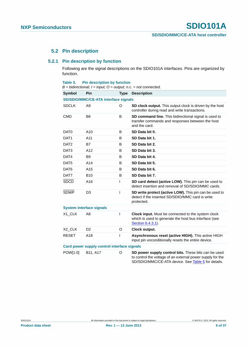
5.2 Pin description
5.2.1 Pin description by function
Following are the signal descriptions on the SDIO101A interfaces. Pins are organized by function.
Table 3. Pin description by functionB = bidirectional; I = input; O = output; n.c. = not connected.
Symbol Pin Type Description
SD/SDIO/MMC/CE-ATA interface signals
SDCLK A9 O SD clock output. This output clock is driven by the host controller during read and write transactions.
CMD B6 B SD command line. This bidirectional signal is used to transfer commands and responses between the host and the card.
DAT0 A10 B SD Data bit 0.
DAT1 A11 B SD Data bit 1.
DAT2 B7 B SD Data bit 2.
DAT3 A12 B SD Data bit 3.
DAT4 B9 B SD Data bit 4.
DAT5 A14 B SD Data bit 5.
DAT6 A15 B SD Data bit 6.
DAT7 B10 B SD Data bit 7.
SDCD A16 I SD card detect (active LOW). This pin can be used to detect insertion and removal of SD/SDIO/MMC cards.
SDWP D3 I SD write protect (active LOW). This pin can be used to detect if the inserted SD/SDIO/MMC card is write protected.
System interface signals
X1_CLK A8 I Clock input. Must be connected to the system clock which is used to generate the host bus interface (see Section 6.4.3.1).
X2_CLK D2 O Clock output.
RESET A18 I Asynchronous reset (active HIGH). This active HIGH input pin unconditionally resets the entire device.
Card power supply control interface signals
POW[1:0] B11, A17 O SD power supply control bits. These bits can be used to control the voltage of an external power supply for the SD/SDIO/MMC/CE-ATA device. See Table 5 for details.
SDIO101A All information provided in this document is subject to legal disclaimers. © NXP B.V. 2013. All rights reserved.
Product data sheet Rev. 1 — 13 June 2013 6 of 37

NXP Semiconductors SDIO101ASD/SDIO/MMC/CE-ATA host controller
[1] HXQFN60 package die supply ground is connected to both GND pins and exposed center pad. GND pins must be connected to supply ground for proper device operation. For enhanced thermal, electrical, and board level performance, the exposed pad needs to be soldered to the board using a corresponding thermal pad on the board and for proper heat conduction through the board, thermal vias need to be incorporated in the PCB in the thermal pad region.
Host Interface control signals
CS A19 I Chip Select (active LOW).
A[7:1] B1, A1, D1, D5, A32, B20, A31
I Address lines. Can be used to address the 256 bytes of the Standard Host register space.
A8 B2 I Address 8. When accessing SDIO101A transmit or receive buffer under DMA control, this pin must be HIGH. This pin must be LOW when accessing other registers or when accessing transmit or receive buffer under interrupt control.
D[15:0] A30, B19, A29, B18, A28, A27, B17, A21, A26, D4, D8, A24, B15, A23, A22, B14
B Data lines. Used to transfer data between host controller and the processor.
RE A2 I Read Enable (active LOW). Initiates a read transaction when active.
WE B13 I Write Enable (active LOW). Initiates a write transaction when active.
BE[1:0] A5, B3 I Byte write enables (active LOW). When BE[0] is active, the least significant byte on the data bus can be written. When BE[1] is active, the most significant byte on the data bus can be written.
INT B4 O Interrupt request (active LOW). Can be configured as push/pull or open-collector output.
DREQ A6 O DMA request.
Power interface signals
VDD A4 - Core power supply pin, 1.8 V.
VDDA A7 - Analog power supply, 1.8 V.
VDD(SD) D6, B8, D7 - SD power supply pins, 1.8 V to 3.3 V.
VDD(IO) B12, B16, A3 - Host interface power supply pins, 2.5 V to 3.3 V.
GND B5, A13, A20, A25[1]
- Ground.
GND center pad[1] - Ground.
Table 3. Pin description by function …continuedB = bidirectional; I = input; O = output; n.c. = not connected.
Symbol Pin Type Description
SDIO101A All information provided in this document is subject to legal disclaimers. © NXP B.V. 2013. All rights reserved.
Product data sheet Rev. 1 — 13 June 2013 7 of 37

NXP Semiconductors SDIO101ASD/SDIO/MMC/CE-ATA host controller
6. Functional description
The SDIO101A offers the SD Standard Host register set as defined in the SD Host Standard Specification Version 2.0 (see Ref. 1), through which the Host Driver software can configure the host controller and initiate transactions to and from an SD/SDIO/MMC/CE-ATA target. On top of the Standard Host registers, 4 extra registers are available in the Host Controller register space, which can be used to control the additional features in the SDIO101A. These features are described in detail in Section 6.4. Section 6.2 gives an overview of the SDIO101A register set.
6.1 DMA mode
The SDIO101A supports slave DMA where the transferring of data between the host and the SDIO101A is under the control of the host’s DMA controller. In this mode, the software can program DMA burst size (number of 16-bit words per DMA cycle) as well as the delay between back-to-back DMA requests from SDIO101A.
In DMA mode, Buffer Data Port 0 (0x20) and Buffer Data Port 1 (0x22) are mapped differently than in Interrupt mode — address line A8 must be at logic 1 when Buffer Data Ports are being accessed while the rest of the address lines are ignored by the SDIO101A. Once the DMA operation starts, all the accesses to the SDIO101A with A8 set to logic 1 will be considered as Buffer Data Ports access. To access other SDIO101A internal registers, address A8 must be set to logic 0.
The total number of DMA accesses to the Buffer Data Ports must be an even number. The first access from the host will be to Buffer Data Port 0, and the second access will be to Buffer Data Port 1. The SDIO101A will automatically alternate between Buffer Data Port 0 and Buffer Data Port 1 on each access by the host. This scheme allows the SDIO101A Buffer Data Ports to look like a continuous block of memory or FIFO to the DMA controller.
There are two registers that must be programmed for the SDIO101A to support DMA operation:
• Miscellaneous register (0xF8) bit 1 (enable slave DMA) must be set to logic 1.
• DMA burst size and DMA inter delay (back-to-back DREQs) must be programmed through DMA register (0xF4). DMA register bit [8:0] programs the DMA burst size (the number of 16-bit words to be transferred between the DMA controller and the SDIO101A), and DMA register bit [15:9] programs the delay time between two back-to-back DMA requests from SDIO101A (the inter delay value in bit [15:9] represents the number of SD clocks).
6.1.1 DMA read
When the receive buffer is empty, DREQ is at LOW state. Once the receive buffer has at least the number of 16-bit words equal to the programmed DMA burst size (DMA register [8:0]) DREQ goes HIGH. The DMA controller then can perform a block read of the receive buffer with the block size equal to the programmed DMA burst size in the DMA register.
The DREQ will go LOW once a block of data has been read from the SDIO101A’s receive buffer, and DREQ will remain LOW for a period defined by DMA register bit [15:9]. The DREQ signal will go HIGH again if the receive buffer still holds at least the burst size of 16-bit word data.
SDIO101A All information provided in this document is subject to legal disclaimers. © NXP B.V. 2013. All rights reserved.
Product data sheet Rev. 1 — 13 June 2013 8 of 37

NXP Semiconductors SDIO101ASD/SDIO/MMC/CE-ATA host controller
6.1.2 DMA write
When the transmit buffer is empty, DREQ is at HIGH state. The DMA controller then can perform a block write to the receive buffer with the block size equal to the programmed DMA burst size programmed in DMA register [9:0].
The DREQ will go LOW once a block of data has been written to the SDIO101A’s transmit buffer, and DREQ will remain LOW for a period defined by DMA register bit [15:9]. The DREQ signal will go HIGH again if the transmit buffer still has space to hold at least the burst size of 16-bit word data.
6.2 Standard Host register overview
[1] This register is not part of the Standard Host register set.
Table 4. SD Host Controller register map
Offset Bits 15:8 Bits 7:0 Offset Bits 15:8 Bits 7:0
0x02 System Address (high) 0x00 System Address (low)
0x06 Block Count 0x04 Block Size
0x0A Argument1 0x08 Argument0
0x0E Command 0x0C Transfer Mode
0x12 Response1 0x10 Response0
0x16 Response3 0x14 Response2
0x1A Response5 0x18 Response4
0x1E Response7 0x1C Response6
0x22 Buffer Data Port1 0x20 Buffer Data Port 0
0x26 Present State 0x24 Present State
0x2A Wake-up Control Block Gap Control 0x28 Power Control Host Control
0x2E Software Reset Time-out Control 0x2C Clock Control
0x32 Error Interrupt Status 0x30 Normal Interrupt Status
0x36 Error Interrupt Status Enable 0x34 Normal Interrupt Status Enable
0x3A Error Interrupt Signal Enable 0x38 Normal Interrupt Signal Enable
0x3E reserved 0x3C Auto CMD12 Error Status
0x42 Capabilities 0x40 Capabilities
0x46 Capabilities (reserved) 0x44 Capabilities (reserved)
0x4A Maximum Current Capabilities 0x48 Maximum Current Capabilities
0x4E Maximum Current Capabilities (reserved)
0x4C Maximum Current Capabilities (reserved)
0x52 (reserved) 0x50[1] IO-cell Configuration
- - - -
0xF6[1] Secondary Clock Control 0xF4[1] DMA register
0xFA[1] PLL 0xF8[1] Miscellaneous
0xFE Host Controller Version 0xFC Slot Interrupt Status
SDIO101A All information provided in this document is subject to legal disclaimers. © NXP B.V. 2013. All rights reserved.
Product data sheet Rev. 1 — 13 June 2013 9 of 37
NXP Semiconductors SDIO101ASD/SDIO/MMC/CE-ATA host controller
6.3 Standard Host register set description
The SDIO101A registers that are part of the Standard Host register set are described in detail in Ref. 1. In this paragraph, we will only describe the specific implementation of the Standard register set in the SDIO101A that are different from Ref. 1.
6.3.1 System Address register (offset 0x00)
Since master-DMA functionality is not implemented, all bits in this register will always read zero. Writes to this register will be ignored.
6.3.2 Block Size register (offset 0x04)
Data written to bits R[14:12] will be ignored. The maximum block size that can be programmed is 1 kB. Any block size higher than that will default to 1 kB.
6.3.3 Transfer Mode register (offset 0x0C)
Since master-DMA functionality is not implemented, bit R[00] will always read zero. Writes to this bit will be ignored.
6.3.4 Present State register (offset 0x24)
The SDIO101A supports multiple buffers, that is, the available data buffer space (2 kB) is larger than the Maximum Block Size (1 kB). The Buffer Write Enable bit R[10] indicates that there is room to write at least one more single block length (as specified in the Block Size register) in the data buffer even though previously-written blocks might still be present. Similarly, the Buffer Read Enable R[11] bit indicates that there is at least one single block length (as specified in the Block Size register) available in the data buffer.
6.3.5 Host Control register (offset 0x28)
A separate LED control pin SDLD is not supported in the SDIO101A. If desired, the user can use a GPIO pin on the Host Processor to implement this functionality. Bit R[00] in the Host Control register will always read zero, and writing to it will have no effect.
6.3.6 Power Control register (offset 0x29)
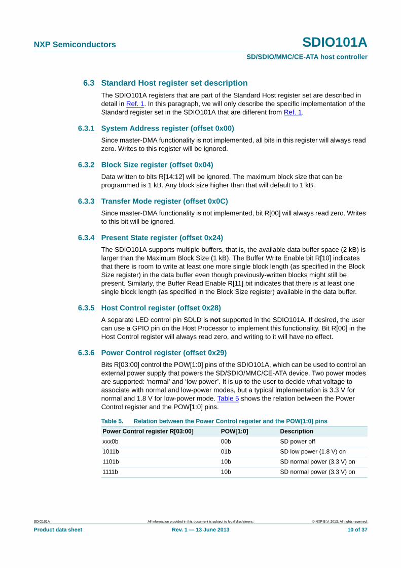
Bits R[03:00] control the POW[1:0] pins of the SDIO101A, which can be used to control an external power supply that powers the SD/SDIO/MMC/CE-ATA device. Two power modes are supported: ‘normal’ and ‘low power’. It is up to the user to decide what voltage to associate with normal and low-power modes, but a typical implementation is 3.3 V for normal and 1.8 V for low-power mode. Table 5 shows the relation between the Power Control register and the POW[1:0] pins.
Table 5. Relation between the Power Control register and the POW[1:0] pins
Power Control register R[03:00] POW[1:0] Description
xxx0b 00b SD power off
1011b 01b SD low power (1.8 V) on
1101b 10b SD normal power (3.3 V) on
1111b 10b SD normal power (3.3 V) on
SDIO101A All information provided in this document is subject to legal disclaimers. © NXP B.V. 2013. All rights reserved.
Product data sheet Rev. 1 — 13 June 2013 10 of 37

NXP Semiconductors SDIO101ASD/SDIO/MMC/CE-ATA host controller
6.3.7 Capabilities register (offset 0x40)
The SDIO101A Capabilities register contents are shown in Table 6.
6.4 Additional register set description
The additional registers are not part of the SD Host Standard Specification Version 2.0 (see Ref. 1). These registers do not have to be initialized, so Standard Host Driver software does not have to be aware of them.
6.4.1 IO Configuration register (offset 0x50)
The IO Configuration register offers three bits to set the drive strength of the IO cell used for driving the SDCLK pin. This way the user can adjust SDCLK rise/fall times according to their system performance requirements. Typically, drive strength should be set to LOW when the SD slot is operating on normal (2.7 V to 3.3 V) voltage, and to HIGH when the SD slot is operating on low voltage (1.8 V). Also, a bit is offered to disable the default pull-up resistors on the SD CMD and SD DATn lines, in case they are not required and the possible leakage current through these resistors is undesired.
Table 6. Contents of the Capabilities register (offset 0x40)
Location Attribute Default Description
63:30 reserved 00h reserved
29 reserved 1b reserved
28 reserved 1b reserved
27 reserved 1b reserved
26 R 1b low voltage (1.8 V) supported
25 R 0b 3.0 V not supported (defaults to normal voltage)
24 R 1b normal voltage (3.3 V) supported
23 R 1b suspend/resume supported
22 R 0b master DMA not supported
21 R 1b high-speed SD (> 25 MHz) supported
20:18 R 001b 8-bit supported
17:16 R 10b 2 kB maximum block length
15:14 reserved 00h reserved
13:08 R 00h get info through other method (Ref. 1)
07 R 1b time-out clock unit in MHz
06 reserved 0b reserved
05:00 R 00h get info through other method (Ref. 1)
Fig 4. IO Configuration register
D00
002aac757
D03 D02 D01
SDCLKdrive strength
SD PU enable
D06 D05 D04D09 D08 D07D12 D11 D10D15 D14 D13
reserved
SDIO101A All information provided in this document is subject to legal disclaimers. © NXP B.V. 2013. All rights reserved.
Product data sheet Rev. 1 — 13 June 2013 11 of 37

NXP Semiconductors SDIO101ASD/SDIO/MMC/CE-ATA host controller
6.4.2 DMA register (offset 0xF4)
The DMA register is located in the Common register area. This register controls the DREQ output. The DREQ LOW and HIGH times are programmed with DMA inter delay and DMA burst size.
Remark: Refer to Section 6.1 for more detailed DMA description.
Table 7. Contents of the IO Configuration register (offset 0x50)
Location Attribute Default Description
15:04 reserved 0h reserved
03:01 R/W 0h SDCLK drive strength select. These bits can be used to program the drive strength of the SDCLK IO cell. Table 8 shows the possible values.
00 R/W 0b SD line pull-up. If set to b1, the internal pull-up resistors on the SD CMD and SD DATn lines are switched ON.
Table 8. SDCLK drive strength programming
IO Configuration register R[03:01] SDCLK drive strength
000b low (SD operating on 2.7 V to 3.6 V)
0001b reserved
010b reserved
011b reserved
100b high (SD operating on 1.8 V)
101b reserved
110b reserved
111b reserved
Fig 5. DMA register
Table 9. DREQ control programming
Location Attribute Default Description
15:09 R/W 0h DREQ delay period (DREQ LOW time)
LOW time = value SD clock cycle time
08:01 R/W 0h DMA burst size (DREQ HIGH time)
D00
002aad321
D03 D02 D01
DMA burst size
D06 D05 D04D09 D08 D07D12 D11 D10D15 D14 D13
DREQ inter delay
SDIO101A All information provided in this document is subject to legal disclaimers. © NXP B.V. 2013. All rights reserved.
Product data sheet Rev. 1 — 13 June 2013 12 of 37

NXP Semiconductors SDIO101ASD/SDIO/MMC/CE-ATA host controller
6.4.3 Secondary Clock Control register (offset 0xF6)
The Secondary Clock Control register is located in the Common register area. This register gives the user more control over the clock generation. An additional fractional divider is offered to program the SDCLK base frequency with higher granularity, allowing the design to use an existing (available) clock rather than an external crystal or oscillator. Figure 6 shows the architecture of the secondary clock control.
The SDCLK base frequency can be calculated with Equation 11:
(1)
Where ‘divisor’ is the standard divisor as programmed in the Clock Control register; N is the integer divisor as programmed in the Secondary Clock Control register R[07:00]; M is the fractional divisor as programmed in the Secondary Clock Control register R[11:08]. Figure 7 and Table 10 below show the register bits of the Secondary Clock Control register.
(1) Divisor is set by the Clock Control register (0x2C).
Fig 6. Secondary clock control architecture
002aac758
SECONDARY CLOCKCONTROL REGISTER
bypass
PLL REGISTER
fPLLfosc PLLfosc × (B + 1)
B P
CRYSTALOSCILLATOR
X1_CLK
X2_CLK
FRACTIONALDIVIDER
fPLL
N + M16
N M
SD SLOT 1CLOCK CONTROL
REGISTER
fSDCLK(base)
divisor
DIVIDERF/divisor(1)
SD CONTROLLER
F
1. This is the average SD clock frequency. The peak SD clock frequency might be higher when the fractional divisor M is used.
Fig 7. Secondary Clock Control register
Table 10. Contents of the Secondary Clock Control register (offset 0xF6)
Location Attribute Default Description
15:12 reserved 00h reserved
11:08 R/W 00h fractional divisor value M
07:00 R/W 01h integer divisor value N
fSDCLK base fPLL
divisor NM16------+
-----------------------------------------=
D00
002aac759
D03 D02 D01
integer divisor N
D06 D05 D04D09 D08 D07D12 D11 D10D15 D14 D13
reserved fractional divisor M
SDIO101A All information provided in this document is subject to legal disclaimers. © NXP B.V. 2013. All rights reserved.
Product data sheet Rev. 1 — 13 June 2013 13 of 37

NXP Semiconductors SDIO101ASD/SDIO/MMC/CE-ATA host controller
6.4.3.1 SDIO101A X1_CLK input
It is recommended that the SDIO101A’s input clock be connected to one of the systems available clock sources to eliminate the use of an external crystal. The best use case is to have the SDIO101A’s X1_CLK input be connected to the processor’s clock output (Figure 8) or processor’s crystal output (Figure 9). In either case, the SDIO101A internal PLL can be used to boost up the X1_CLK input then divided down to the desired SDIO clock by using the internal divider in combination with the built-in fractional divider.
Figure 10 details a typical scenario where the host processor uses a 13 MHz crystal as its clock source, and the same clock is used by the SDIO101A to operate the SD clock as close to 50 MHz as possible.
With its input clock supplies by the processor crystal output, the SDIO101A internal PLL (0xFA) is used to boost the input frequency to 104 MHz, the standard Clock Control register (0x2C) and the fractional divider (0xF6) registers are then used to divide the 104 MHz to about 48.9 MHz to be used as SD clock.
Fig 8. X1_CLK connected to processor’s system clock
Fig 9. X1_CLK connected to processor crystal clock output
Fig 10. Host processor using 13 MHz crystal as clock source
002aah562
PROGRAMMABLEOSCILLATOR
DIVIDER
X1_CLKclock in
HOST
CPU clock
clock out
SDIO101A
002aah563
X1_CLK
HOST SDIO101AX1 X2
002aah564
X1_CLK
HOST SDIO101AX1 X2
13 MHz
SDIO101A All information provided in this document is subject to legal disclaimers. © NXP B.V. 2013. All rights reserved.
Product data sheet Rev. 1 — 13 June 2013 14 of 37

NXP Semiconductors SDIO101ASD/SDIO/MMC/CE-ATA host controller
PLL register (0xFA) settings:
Bit 15 = 0b
Bit 14 = 0b
Bit [13:7] = 0000000b
Bit [6:5] = 01b
Bit [4:0] = 00111b; B = 7
Fractional divider (0xF6) settings:
Bit [15:12] = 0000b; reserved bit
Bit [11:8] = 0001b; M = 1
Bit [7:0] = 00000001b; N = 1
Clock Control register (0x2C) settings:
Bit [15:0] = 103h
= (13 MHz 8) / (2 (1 + 1 / 16))
= 48.9 MHz
6.4.4 Miscellaneous register (offset 0xF8)
The Miscellaneous register is located in the Common register area. This register can be programmed to put the device in the ‘Coma mode’ or ‘Hibernate mode’, extra-low power-down modes on top of the Standby mode programmable through bit R[00] in the Clock Control register. Also, a bit is offered to disable the DREQ DMA request line on the Host Interface. Lastly, a bit is offered to switch between open-drain and push-pull mode for the INT interrupt output pin. Figure 11 and Table 11 below show the register bits of the Miscellaneous register.
fSDCLK base fPLL
divisor NM16------+
-------------------------------------------=
Fig 11. Miscellaneous register
D00
002aac761
D03 D02 D01D06 D05 D04D09 D08 D07D12 D11 D10D15 D14 D13
reserved
slave DMA enable
Coma mode
INT mode
Hibernate mode
SDIO101A All information provided in this document is subject to legal disclaimers. © NXP B.V. 2013. All rights reserved.
Product data sheet Rev. 1 — 13 June 2013 15 of 37

NXP Semiconductors SDIO101ASD/SDIO/MMC/CE-ATA host controller
6.4.5 PLL register (offset 0xFA)
The PLL register is located in the Common register area. This register provides control over the Phase-Locked Loop, which is used in the SDIO101A to generate an SD base clock frequency from the crystal oscillator or external clock source. The default values of this register are such that the PLL multiplies the incoming frequency from the crystal oscillator by 5. This means that, if the PLL register is not programmed, the frequency generated by the crystal oscillator or external clock source should be 10.4 MHz in order to generate the 52 MHz maximum SDCLK speed. For the SD base clock frequency generated by the PLL from the Crystal oscillator frequency it holds
(2)
where B is the feedback divider value as programmed in R[04:00] of the PLL register. The user should determine the desired fPLL, choose the required value B for the feedback divider based on the available clock source fosc, and then choose a value for post divider P (as programmed in R[06:05]) such that the following condition gets satisfied:
(3)
The post divider setting decided by the value of P does not affect the frequency value (in MHz) of the fPLL. The only advantage of this post divider is in adjusting the duty cycle of the resulting fPLL clock. The greater the value of P, the closer the duty cycle will be to 50 % (provided the condition mentioned in Equation 3 is not violated, for a guaranteed behavior).
The PLL register also provides the possibility to bypass the PLL post divider, effectively setting a value of 1 for P. Also, the user can bypass the entire PLL. Figure 12 and Table 12 show the register bits of the PLL register.
Table 11. Contents of the Miscellaneous register (offset 0xF8)
Location Attribute Default Description
15:04 reserved 00h reserved
03 R/W 0b Hibernate mode select. When set to 1b, the oscillator, PLL and supply to the buffer memory will be switched OFF. Card detection is disabled. Clearing this bit will re-instate power to the buffer memory, the oscillator and PLL are enabled.
02 R/W 0b INT mode select. When set to 0b, the INT interrupt output pin will be open-drain mode. An external 10 k pull-up resistor is required in this case. When set to 1b, the INT interrupt output pin will be in push-pull mode.
01 R/W 1b Slave DMA enable. If programmed to 1b, the DREQ signal will be functional. If programmed to 0b, the DREQ signal will be fixed to zero.
00 R/W 0b Coma mode. If programmed to 1b, power will internally be switched off to most of the device, resulting in a very low coma mode current. All state in the device will be lost, and no registers can be read or written, with the exception of the ‘Software Reset for All’ bit in the Software Reset register. Clearing this bit will re-instate power to the entire chip, and reset the SDIO101A. A hard-reset on the RESET pin will also bring the device back out of Coma mode.
fPLL B 1+ f= CLK
156 MHz 2 P 1+ fPLL 320 MHz
SDIO101A All information provided in this document is subject to legal disclaimers. © NXP B.V. 2013. All rights reserved.
Product data sheet Rev. 1 — 13 June 2013 16 of 37

NXP Semiconductors SDIO101ASD/SDIO/MMC/CE-ATA host controller
6.4.6 Host Controller Version register (offset 0xFE)
The SDIO101A Host Controller version is shown in Table 13.
[1] These bits do not match Host Controller specification. Host driver should not use these bits.
Fig 12. PLL register
Table 12. Contents of the PLL register (offset 0xFA)
Location Attribute Default Description
15 R/W 1b PLL bypass. If this bit is 1b, the PLL is bypassed. The SDCLK base frequency is then equal to the frequency provided by the oscillator, either generated by a crystal or generated by an external clock. If this bit is 0b, the PLL is not bypassed.
14 R/W 1b PLL direct. If this bit is 1b, the post divider of the PLL is bypassed, effectively setting the post divider value P to 1b. In this mode, the duty cycle out of the PLL can be unequal to 50 %. If set to 0b, the post divider P is used, and its value is determined by R[06:05] of the PLL register.
13:07 reserved 00h reserved
06:05 R/W 01h PLL post divider P
04:00 R/W 04h PLL feedback divider B
D00
002aac760
D03 D02 D01
post dividerP
D06 D05 D04D09 D08 D07D12 D11 D10D15 D14 D13
reserved
PLL bypass
PLL directfeedback divider B
Table 13. Contents of the Host Controller Version register (offset 0xFE)
Location Attribute Default Description
15:08 R 10h SDIO101A version 1.0
07:00 reserved 00h reserved[1]
SDIO101A All information provided in this document is subject to legal disclaimers. © NXP B.V. 2013. All rights reserved.
Product data sheet Rev. 1 — 13 June 2013 17 of 37

NXP Semiconductors SDIO101ASD/SDIO/MMC/CE-ATA host controller
6.5 Power-saving modes
The SDIO101A provides 5 power-saving modes that can be used in different situations to minimize the power consumption of the device. Table 14 below describes these modes and their associated register bits that can be programmed to enable them. Idle, Low Power and Standby modes can be used if card interrupts should still be serviced. The Hibernate mode will switch off the power to the SD device and the Coma mode switches off most of the Host Controller, therefore, card interrupts will not be generated. Table 14 shows the 5 power-saving modes.
7. Application design-in information
Table 14. SDIO101A Power-saving modes
Mode Associated register bits
Description
Idle mode Clock Control register R[02]
SD Card clock stopped; oscillator and PLL are active.
Low-Power mode
Power Control register R[00]
SD Card power switched off.
Standby mode Clock Control register R[00]
When the Clock Control register R[00] is set to b0, the SDIO101A internal clock is stopped, the PLL is in Power-down mode, the oscillator is active and all register states are maintained. The device will still respond to card interrupts. When waking up from Standby mode, after writing a b1 in the Clock Control register R[00], the data buffer FIFO pointers will reset to empty.
Coma mode Miscellaneous register R[00]
When the Miscellaneous register R[00] is set to b1, the SDIO101A internal power is switched off. All device pins are 3-stated, and only a write to the ‘Software Reset for All’ bit in the Software Reset register or a hard reset on the RESET pin will wake up the device. All device states, including data buffer contents, are lost. Card insertion and removal detection through the SDCD pin is disabled.
Hibernate mode
Miscellaneous register R[03]
The oscillator, PLL and supply to the buffer memory will be switched off. All states are maintained, but data buffer contents are lost. Card insertion and removal detection through the SDCD pin is disabled. Upon wake-up, the data buffer FIFO pointers will reset to empty.
Fig 13. Typical application: host and card interface
002aad063
SDIOCORE
HOSTINTERFACE
CARDINTERFACE
VDD(IO) = 3.3 V VDD = 1.8 V VDD(SD) = 1.8 V or 3.3 V
SDIO CONTROLLER
SDPOWERSUPPLY
3.3 V/1.8 V
POW0POW1
CARD
SDIO101A All information provided in this document is subject to legal disclaimers. © NXP B.V. 2013. All rights reserved.
Product data sheet Rev. 1 — 13 June 2013 18 of 37

NXP Semiconductors SDIO101ASD/SDIO/MMC/CE-ATA host controller
8. Basic architecture
The SDIO101A provides SD/SDIO/MMC/CE-ATA functionality to a microprocessor system as illustrated in Figure 14. A standard SD/SDIO/MMC/CE-ATA driver running on the host processor will be able to access the standard host register set in the SDIO101A through the 16-bit memory interface, and initiate transactions to and from the SD card. An external SD power supply (controlled by the SDIO101A) can be used to supply the SD card.
Fig 14. SDIO101A used in a microprocessor application
002aah565
SDIO101A
CS
A[7:1]
D[15:0]
RE
WE
BE[1:0]
INT
DREQ
MICROPROCESSOR
DMACONTROLLER
POW[1:0]
SDCLK
CMD
DAT[7:0]
SDPOWERSUPPLY
VDD VSS
CARD
X1_CLKA8
SDCD
SDWP
SDIO101A All information provided in this document is subject to legal disclaimers. © NXP B.V. 2013. All rights reserved.
Product data sheet Rev. 1 — 13 June 2013 19 of 37
NXP Semiconductors SDIO101ASD/SDIO/MMC/CE-ATA host controller
9. Limiting values
10. Recommended operating conditions
[1] If the PLL is not bypassed, the minimum input frequency is 10 MHz.
Table 15. Limiting valuesIn accordance with the Absolute Maximum Rating System (IEC 60134).
Symbol Parameter Conditions Min Max Unit
VDD(IO) input/output supply voltage host interface; in 2.5 V to 3.3 V range
0.3 +4.6 V
VDD(SD) SD supply voltage SD interface
in 1.8 V range 0.3 +1.95 V
in 3.3 V range 0.3 +3.6 V
VDD supply voltage core; 1.8 V range 0.3 +2.4 V
VI input voltage on any input pin
1.8 V interface VSS 0.3 VDD + 0.6 V
3.3 V interface 0.3 +3.6 V
Tamb ambient temperature operating 40 +85 C
Tstg storage temperature 65 +150 C
VESD electrostatic discharge voltage SD/MMC/SDIO interface; Human Body Model
4 +4 kV
Table 16. Operating conditions
Symbol Parameter Conditions Min Typ Max Unit
VDD supply voltage core 1.65 1.8 1.95 V
VDD(IO) input/output supply voltage host interface 2.25 3.3 3.6 V
VDD(SD) SD supply voltage SD interface 1.65 3.3 3.6 V
fclk(ext) external clock frequency [1] 1 - 52 MHz
IDD(AV) average supply current f = 13 MHz; SDCLK = 25 MHz
- 6 - mA
IDD supply current Standby mode - 460 - A
Hibernate mode - 69 - A
Coma mode - 5 - A
Toper operating temperature 40 +25 +85 C
SDIO101A All information provided in this document is subject to legal disclaimers. © NXP B.V. 2013. All rights reserved.
Product data sheet Rev. 1 — 13 June 2013 20 of 37

NXP Semiconductors SDIO101ASD/SDIO/MMC/CE-ATA host controller
11. Static characteristics
[1] X1_CLK = 3.3 V only.
[2] IDD is the supply on VDD and VDDA.
[3] IDD(IO) current might be higher or lower depending on the activity of the 16-bit data bus. The numbers specified in the data sheet are measured with no activity on the host controller bus. The data bus, address bus and control signals are pulled HIGH.
Table 17. Static characteristics
Symbol Parameter Conditions VDD(IO) = 2.5 V VDD(IO) = 3.3 V Unit
Min Max Min Max
VIL(clk) clock LOW-level input voltage X1_CLK [1] 0.3 +0.6 0.3 +0.6 V
VIH(clk) clock HIGH-level input voltage X1_CLK [1] 2.4 VDD 2.4 VDD V
VIL LOW-level input voltage 0.3 +0.65 0.3 +0.8 V
VIH HIGH-level input voltage 1.6 VDD 2.1 VDD V
VOL LOW-level output voltage IOL = 2 mA - 0.4 - 0.4 V
VOH HIGH-level output voltage IOH = 800 A 1.4 - 2.1 - V
ILIL LOW-level input leakage current - 10 - 10 A
ILIH HIGH-level input leakage current - 10 - 10 A
IL(clk) clock leakage current X1_CLK - 30 - 30 A
Ci input capacitance - 5 - 5 pF
Dynamic average supply current (VDD(SD) = 3.3 V)
IDD(AV) average supply current 25 MHz [2] - 7 - 7 mA
52 MHz [2] - 9 - 9 mA
IDD(IO) input/output supply current 25 MHz [3] - 1.3 - 1.5 mA
52 MHz [3] - 1.3 - 1.5 mA
IDD(SD) SD supply current 25 MHz - 1.5 - 1.5 mA
52 MHz - 2.3 - 2.3 mA
Hibernate mode supply current (VDD(SD) = 3.3 V)
IDD supply current [2] - 130 - 130 A
IDD(IO) input/output supply current 25 MHz [3] - 20 - 20 A
IDD(SD) SD supply current - 1.5 - 1.5 A
Standby mode supply current (VDD(SD) = 3.3 V)
IDD supply current [2] - 4 - 4 mA
IDD(IO) input/output supply current [3] - 20 - 20 A
IDD(SD) SD supply current - 1.5 - 1.5 A
Coma mode supply current (VDD(SD) = 3.3 V)
IDD supply current [2] - 0.6 - 0.6 A
IDD(IO) input/output supply current [3] - 20 - 20 A
IDD(SD) SD supply current - 0.5 - 0.5 A
SDIO101A All information provided in this document is subject to legal disclaimers. © NXP B.V. 2013. All rights reserved.
Product data sheet Rev. 1 — 13 June 2013 21 of 37

NXP Semiconductors SDIO101ASD/SDIO/MMC/CE-ATA host controller
12. Dynamic characteristics
Table 18. Dynamic characteristics for 16-bit host bus interface
Symbol Parameter Conditions VDD(IO) = 2.5 V VDD(IO) = 3.3 V Unit
Min Max Min Max
tWL(X1_CLK) X1_CLK pulse width LOW 9 - 9 - ns
tWH(X1_CLK) X1_CLK pulse width HIGH 9 - 9 - ns
fX1_CLK frequency on pin X1_CLK - 52 - 52 MHz
tsu(A) address set-up time 5 - 5 - ns
th(A) address hold time 10 - 5 - ns
th(WE-CS) hold time from WE to CS 0 - 0 - ns
td(CSL-WEL) delay time from CS LOW to WE LOW 0 - 0 - ns
tw(WE) WE pulse width 10 - 20 - ns
td(WE) WE delay time 10 - 20 - ns
tsu(D-WEH) set-up time from data input to WE HIGH
5 - 5 - ns
th(WEH-D) data input hold time after WE HIGH 5 - 5 - ns
tsu(BEn) set-up time on pin BEn 5 - 5 - ns
th(BEn) hold time on pin BEn 5 - 5 - ns
th(RE-CS) hold time from RE to CS 0 - 0 ns
td(CS-RE) delay time from CS to RE 0 - 0 ns
tw(RE) RE pulse width 25 - 20 ns
td(RE) RE delay time 10 - 10 ns
td(RE-Q) delay time from RE to data output 25 pF load - 20 - 25 ns
tdis(RE-QZ) disable time from RE to high-impedance data output
25 pF load - 20 - 15 ns
tw(RESET) pulse width on pin RESET 10 - 5 - ns
td(buf_full-INTL) delay time from buffer full to INT LOW receive buffer (receive)
- 4XTAL1 - 4XTAL1 ns
td(int_clr-INTH) delay time from interrupt clear to INT HIGH
receive buffer (read)
- 300 - 300 ns
td(buf_emp-INTL) delay time from buffer empty to INT LOW
transmit buffer (transmit)
- 4XTAL2 - 4XTAL2 ns
td(int_clr-INTH) delay time from interrupt clear to INT HIGH
transmit buffer (write)
- 80 - 80 ns
tsu(A8) address 8 set-up time 5 - 5 - ns
tsu(A8-CS) set-up time from address 8 to CS 5 - 5 - ns
td(SDCLK-DREQH) delay time from SDCLK to DREQ HIGH
- 20 - 15 ns
td(CSH-DREQL)W write delay time from CS HIGH to DREQ LOW
- 20 - 15 ns
td(CSH-DREQL)R read delay time from CS HIGH to DREQ LOW
- 20 - 15 ns
SDIO101A All information provided in this document is subject to legal disclaimers. © NXP B.V. 2013. All rights reserved.
Product data sheet Rev. 1 — 13 June 2013 22 of 37

NXP Semiconductors SDIO101ASD/SDIO/MMC/CE-ATA host controller
Table 19. Dynamic characteristics for MMC/SD/SDIO bus interfaceVDD(SD) = 2.7 V to 3.3 V.
Symbol Parameter Conditions 25 MHz 52 MHz Unit
Min Max Min Max
Clock
tWL clock low time 10 pF max. 12 - 8 - ns
tWH clock high time 10 pF max. 12 - 8 - ns
tw(clk) clock pulse width 10 pF max. 40 - 18 - ns
tTLH clock rise time 10 pF max. - 10 - 3 ns
tTHL clock fall time 10 pF max. - 10 - 3 ns
Input CMD, DATn
tISU input set-up time 10 pF max. 5 - 6 - ns
tIH input hold time 10 pF max. 5 - 2 - ns
Output CMD, DATn
tODLY output delay time during data transfer mode; 40 pF max. 0 14 - 14 ns
tOH output hold time 2.5 - 2.5 - ns
Table 20. Dynamic characteristics for MMC/SD/SDIO bus interfaceVDD(SD) = 1.70 V to 1.95 V.
Symbol Parameter Conditions 25 MHz 52 MHz Unit
Min Max Min Max
Clock
tWL clock low time 10 pF max. 12 - 8 - ns
tWH clock high time 10 pF max. 12 - 8 - ns
tw(clk) clock pulse width 10 pF max. 40 - 18 - ns
tTLH clock rise time 10 pF max. - 10 - 3 ns
tTHL clock fall time 10 pF max. - 10 - 3 ns
Input CMD, DATn
tISU input set-up time 10 pF max. 5 - 6 - ns
tIH input hold time 10 pF max. 5 - 2 - ns
Output CMD, DATn
tODLY output delay time during data transfer mode; 40 pF max. 0 14 - 14 ns
tOH output hold time 2.5 - 2.5 - ns
SDIO101A All information provided in this document is subject to legal disclaimers. © NXP B.V. 2013. All rights reserved.
Product data sheet Rev. 1 — 13 June 2013 23 of 37

NXP Semiconductors SDIO101ASD/SDIO/MMC/CE-ATA host controller
12.1 Timing diagrams
Fig 15. 8-bit write
A[7:1]
CS
WE
BE0 to BE1
D[15:0]
tsu(A)
002aad301
tsu(A)
tsu(BEn)
th(A)
th(WE-CS)
td(WE)
th(BEn)
10b
tsu(D-WEH) th(WEH-D)
D[7:0]
01b
D[15:8]
tw(WE)
Fig 16. 16-bit write
A[7:1]
CS
WE
BE0 to BE1
D[15:0]
tsu(A)
002aad302
tsu(A)
tsu(BEn)
th(A)
th(WE-CS)
td(WE)
th(BEn)
00b
tsu(D-WEH) th(WEH-D)
D[15:0]
00b
D[15:0]
tw(WE)
SDIO101A All information provided in this document is subject to legal disclaimers. © NXP B.V. 2013. All rights reserved.
Product data sheet Rev. 1 — 13 June 2013 24 of 37

NXP Semiconductors SDIO101ASD/SDIO/MMC/CE-ATA host controller
Fig 17. 8-bit read
A[7:1]
CS
RE
BE0 to BE1
D[15:0]
tsu(A)
002aad304
tsu(A)
tsu(BEn)
th(A)
th(RE-CS)
td(RE)
th(BEn)
10b
td(RE-Q) tdis(RE-QZ)
D[7:0]
01b
D[15:8]
tw(RE)
Fig 18. 16-bit read
A[7:1]
CS
RE
BE0 to BE1
D[15:0]
tsu(A)
002aad303
tsu(A)
tsu(BEn)
th(A)
th(RE-CS)
td(RE)
th(BEn)
00b
td(RE-Q) tdis(RE-QZ)
D[15:0]
00b
D[15:0]
tw(RE)
SDIO101A All information provided in this document is subject to legal disclaimers. © NXP B.V. 2013. All rights reserved.
Product data sheet Rev. 1 — 13 June 2013 25 of 37

NXP Semiconductors SDIO101ASD/SDIO/MMC/CE-ATA host controller
Fig 19. 25 MHz SDCLK
Fig 20. 55 MHz SDCLK
002aad306
tWL
0.2VDDSDCLK
tw(clk)
tWH
valid
0.7VDD
tTHL
valid
tTLH
DAT[7:0], CMD(input)
DAT[7:0], CMD(output)
tISU tIH
tODLY(max)tODLY(min)
0.7VDD
0.2VDD
002aad305
tWL
0.2VDDSDCLK
tw(clk)
tWH
valid
0.7VDD
tTHL
valid
tTLH
DAT[7:0], CMD(input)
DAT[7:0], CMD(output)
tISU tIH
tODLY
50 % VDD
tOH
0.7VDD
0.2VDD
SDIO101A All information provided in this document is subject to legal disclaimers. © NXP B.V. 2013. All rights reserved.
Product data sheet Rev. 1 — 13 June 2013 26 of 37

NXP Semiconductors SDIO101ASD/SDIO/MMC/CE-ATA host controller
Fig 21. DMA write
Fig 22. DMA read
tsu(A8)
002aad324
A8
A[7:1] DON'T CARE
DREQ
CS
WE
SDCLK
tsu(A8-CS)
1 2 N
DMA burst size
1 2
td(SDCLK-DREQH)
NDMA inter delay
td(CSH-DREQL)W
tsu(A8)
002aad325
A8
A[7:1] DON'T CARE
DREQ
CS
RE
SDCLK
tsu(A8-CS)
1 2 N
DMA burst size
1 2
td(SDCLK-DREQH)
NDMA inter delay
td(CSH-DREQL)R
SDIO101A All information provided in this document is subject to legal disclaimers. © NXP B.V. 2013. All rights reserved.
Product data sheet Rev. 1 — 13 June 2013 27 of 37
NXP Semiconductors SDIO101ASD/SDIO/MMC/CE-ATA host controller
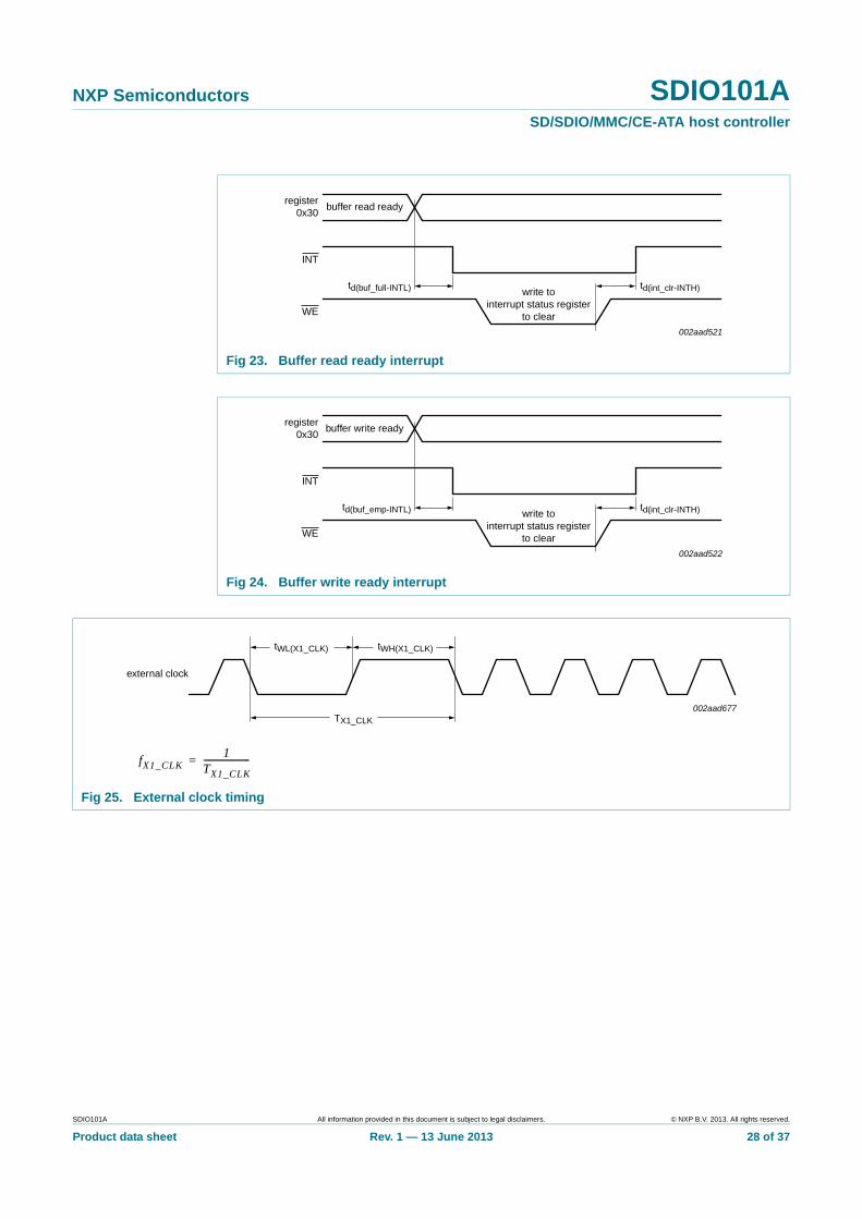
Fig 23. Buffer read ready interrupt
Fig 24. Buffer write ready interrupt
register0x30
INT
WE
td(buf_full-INTL)
002aad521
td(int_clr-INTH)
buffer read ready
write tointerrupt status register
to clear
register0x30
INT
WE
td(buf_emp-INTL)
002aad522
td(int_clr-INTH)
buffer write ready
write tointerrupt status register
to clear
Fig 25. External clock timing
external clock
002aad677TX1_CLK
tWL(X1_CLK) tWH(X1_CLK)
fX1_CLK1
TX1_CLK---------------------=
SDIO101A All information provided in this document is subject to legal disclaimers. © NXP B.V. 2013. All rights reserved.
Product data sheet Rev. 1 — 13 June 2013 28 of 37

NXP Semiconductors SDIO101ASD/SDIO/MMC/CE-ATA host controller
13. Package outline
Fig 26. Package outline SOT1133-2 (HXQFN60)
ReferencesOutlineversion
Europeanprojection Issue date
IEC JEDEC JEITA
SOT1133-2 - - -- - -- - -
sot1133-2_po
11-09-1611-11-24
Unit
mmmaxnommin
0.50 0.080.050.02
0.280.230.18
2.952.852.75
5.055.004.95
2.952.852.75
2.0 3.5 3.50.170.120.07
0.1
A
Dimensions
HXQFN60: plastic compatible thermal enhanced extremely thin quad flat package; no leads;60 terminals; body 5 x 5 x 0.5 mm SOT1133-2
A1 A2
0.420.400.38
b D
5.055.004.95
Dh E Eh
0.08 0.1
y y1e
0.5
e1 e2 e3
2.0
e4 eT
0.515
eR
0.525
K
0.250.200.15
L
0.280.230.18
L1 v
0.05
w
0 5 mm
scale
terminal 1index area
B AD
E
C
yCy1
X
detail X
A A2
A1
terminal 1index area
e2
e1
eTeR
eT
eR
e4e3
e
e
1/2 e
1/2 eAC Bv
Cw
bAC Bv
Cw
Dh
K
L
Eh
L1
B1
A1
B5
D5 D8
D6 D7
D1 D4
D2 D3
B20 B16A25
A24
A17
B11
B15
A9B6 B10
A16
A32
A8
eR
eT
eReT
SDIO101A All information provided in this document is subject to legal disclaimers. © NXP B.V. 2013. All rights reserved.
Product data sheet Rev. 1 — 13 June 2013 29 of 37
NXP Semiconductors SDIO101ASD/SDIO/MMC/CE-ATA host controller
14. Soldering of SMD packages
This text provides a very brief insight into a complex technology. A more in-depth account of soldering ICs can be found in Application Note AN10365 “Surface mount reflow soldering description”.
14.1 Introduction to soldering
Soldering is one of the most common methods through which packages are attached to Printed Circuit Boards (PCBs), to form electrical circuits. The soldered joint provides both the mechanical and the electrical connection. There is no single soldering method that is ideal for all IC packages. Wave soldering is often preferred when through-hole and Surface Mount Devices (SMDs) are mixed on one printed wiring board; however, it is not suitable for fine pitch SMDs. Reflow soldering is ideal for the small pitches and high densities that come with increased miniaturization.
14.2 Wave and reflow soldering
Wave soldering is a joining technology in which the joints are made by solder coming from a standing wave of liquid solder. The wave soldering process is suitable for the following:
• Through-hole components
• Leaded or leadless SMDs, which are glued to the surface of the printed circuit board
Not all SMDs can be wave soldered. Packages with solder balls, and some leadless packages which have solder lands underneath the body, cannot be wave soldered. Also, leaded SMDs with leads having a pitch smaller than ~0.6 mm cannot be wave soldered, due to an increased probability of bridging.
The reflow soldering process involves applying solder paste to a board, followed by component placement and exposure to a temperature profile. Leaded packages, packages with solder balls, and leadless packages are all reflow solderable.
Key characteristics in both wave and reflow soldering are:
• Board specifications, including the board finish, solder masks and vias
• Package footprints, including solder thieves and orientation
• The moisture sensitivity level of the packages
• Package placement
• Inspection and repair
• Lead-free soldering versus SnPb soldering
14.3 Wave soldering
Key characteristics in wave soldering are:
• Process issues, such as application of adhesive and flux, clinching of leads, board transport, the solder wave parameters, and the time during which components are exposed to the wave
• Solder bath specifications, including temperature and impurities
SDIO101A All information provided in this document is subject to legal disclaimers. © NXP B.V. 2013. All rights reserved.
Product data sheet Rev. 1 — 13 June 2013 30 of 37

NXP Semiconductors SDIO101ASD/SDIO/MMC/CE-ATA host controller
14.4 Reflow soldering
Key characteristics in reflow soldering are:
• Lead-free versus SnPb soldering; note that a lead-free reflow process usually leads to higher minimum peak temperatures (see Figure 27) than a SnPb process, thus reducing the process window
• Solder paste printing issues including smearing, release, and adjusting the process window for a mix of large and small components on one board
• Reflow temperature profile; this profile includes preheat, reflow (in which the board is heated to the peak temperature) and cooling down. It is imperative that the peak temperature is high enough for the solder to make reliable solder joints (a solder paste characteristic). In addition, the peak temperature must be low enough that the packages and/or boards are not damaged. The peak temperature of the package depends on package thickness and volume and is classified in accordance with Table 21 and 22
Moisture sensitivity precautions, as indicated on the packing, must be respected at all times.
Studies have shown that small packages reach higher temperatures during reflow soldering, see Figure 27.
Table 21. SnPb eutectic process (from J-STD-020D)
Package thickness (mm) Package reflow temperature (C)
Volume (mm3)
< 350 350
< 2.5 235 220
2.5 220 220
Table 22. Lead-free process (from J-STD-020D)
Package thickness (mm) Package reflow temperature (C)
Volume (mm3)
< 350 350 to 2000 > 2000
< 1.6 260 260 260
1.6 to 2.5 260 250 245
> 2.5 250 245 245
SDIO101A All information provided in this document is subject to legal disclaimers. © NXP B.V. 2013. All rights reserved.
Product data sheet Rev. 1 — 13 June 2013 31 of 37

NXP Semiconductors SDIO101ASD/SDIO/MMC/CE-ATA host controller
For further information on temperature profiles, refer to Application Note AN10365 “Surface mount reflow soldering description”.
MSL: Moisture Sensitivity Level
Fig 27. Temperature profiles for large and small components
001aac844
temperature
time
minimum peak temperature= minimum soldering temperature
maximum peak temperature= MSL limit, damage level
peak temperature
SDIO101A All information provided in this document is subject to legal disclaimers. © NXP B.V. 2013. All rights reserved.
Product data sheet Rev. 1 — 13 June 2013 32 of 37

NXP Semiconductors SDIO101ASD/SDIO/MMC/CE-ATA host controller
15. Appendix
15.1 Errata
This errata describes the functional behavior deviation of the SDIO101A from the data sheet Rev. 1.
15.1.1 Card detection in Hibernate mode or Coma mode
Card detection does not work when the device is in Coma mode or Hibernate mode. When put in these modes, the SDIO101A SD supply is powered down. When a card is inserted, the card detection circuit will not be able to detect the card because there is no power.
Workaround: If the card is to be put in Hibernate mode or Coma mode, a processor’s GPIO pin with a pull-up resistor can be used to do card detect function. The pin is to be programmed as input, and set to interrupt on both edges. When a card is inserted, this GPIO pin will be pulled LOW by the card and an interrupt is generated. When a card is removed, this GPIO pin will be pulled HIGH by the pull-up resistor and an interrupt is generated.
15.1.2 SD side data rate limitation at 1.8 V
The current device does not work at 52 MHz when the VDD(SD) supply is at 1.8 V. When powered at 1.8 V, the SD side works up to about 30 MHz. (Please note that when VDD(SD) is 2.5 V to 3.3 V, there is no data rate limitation and the device works up to 52 MHz).
Workaround: There is no known workaround solution for this issue, if the card is to be used at 52 MHz with 1.8 V supply. To run the card at 52 MHz, VDD(SD) must be powered at 2.5 V minimum.
15.1.3 High current on VDD pin after power-up
After power-up, VDD pin draws close to 2 mA then the current slowly drops down to the idle current state at 68 A in about 40 seconds. This issue does not have any effect on the normal operation of the device, and the high current only occurs just after the device is powered up.
Workaround: We are investigating this issue to find out what might cause this problem. And, since the issue does not alter the behavior of the device and a root cause has not been identified, there is not a workaround for this issue at this time.
SDIO101A All information provided in this document is subject to legal disclaimers. © NXP B.V. 2013. All rights reserved.
Product data sheet Rev. 1 — 13 June 2013 33 of 37

NXP Semiconductors SDIO101ASD/SDIO/MMC/CE-ATA host controller
16. Abbreviations
17. References
[1] SD Specifications Part A2, SD Host Controller Standard Specification, Version 2.00, February 2007
[2] SD Specifications Part E1, SDIO Specification, Version 2.00, February 8, 2007
[3] SD Specifications Part 1, Physical Layer Specification, Version 2.0, May 9, 2006
[4] The Multimedia Card, System Specification Version 4.1
[5] CE-ATA Digital Protocol, Version 1.1
18. Revision history
Table 23. Abbreviations
Acronym Description
CE-ATA Consumer Electronics Advanced Technology Attachment
CPU Central Processing Unit
DMA Direct Memory Access
FIFO First In, First Out
GPIO General Purpose Input/Output
IO Input/Output
kB kiloByte
LED Light Emitting Diode
MMC Multi-Media Card
PCB Printed-Circuit Board
PLL Phase-Locked Loop
PU Pull-Up
SD Secure Digital
SDIO Secure Digital Input/Output
Table 24. Revision history
Document ID Release date Data sheet status Change notice Supersedes
SDIO101A v.1 20130613 Product data sheet - -
SDIO101A All information provided in this document is subject to legal disclaimers. © NXP B.V. 2013. All rights reserved.
Product data sheet Rev. 1 — 13 June 2013 34 of 37

NXP Semiconductors SDIO101ASD/SDIO/MMC/CE-ATA host controller
19. Legal information
19.1 Data sheet status
[1] Please consult the most recently issued document before initiating or completing a design.
[2] The term ‘short data sheet’ is explained in section “Definitions”.
[3] The product status of device(s) described in this document may have changed since this document was published and may differ in case of multiple devices. The latest product status information is available on the Internet at URL http://www.nxp.com.
19.2 Definitions
Draft — The document is a draft version only. The content is still under internal review and subject to formal approval, which may result in modifications or additions. NXP Semiconductors does not give any representations or warranties as to the accuracy or completeness of information included herein and shall have no liability for the consequences of use of such information.
Short data sheet — A short data sheet is an extract from a full data sheet with the same product type number(s) and title. A short data sheet is intended for quick reference only and should not be relied upon to contain detailed and full information. For detailed and full information see the relevant full data sheet, which is available on request via the local NXP Semiconductors sales office. In case of any inconsistency or conflict with the short data sheet, the full data sheet shall prevail.
Product specification — The information and data provided in a Product data sheet shall define the specification of the product as agreed between NXP Semiconductors and its customer, unless NXP Semiconductors and customer have explicitly agreed otherwise in writing. In no event however, shall an agreement be valid in which the NXP Semiconductors product is deemed to offer functions and qualities beyond those described in the Product data sheet.
19.3 Disclaimers
Limited warranty and liability — Information in this document is believed to be accurate and reliable. However, NXP Semiconductors does not give any representations or warranties, expressed or implied, as to the accuracy or completeness of such information and shall have no liability for the consequences of use of such information. NXP Semiconductors takes no responsibility for the content in this document if provided by an information source outside of NXP Semiconductors.
In no event shall NXP Semiconductors be liable for any indirect, incidental, punitive, special or consequential damages (including - without limitation - lost profits, lost savings, business interruption, costs related to the removal or replacement of any products or rework charges) whether or not such damages are based on tort (including negligence), warranty, breach of contract or any other legal theory.
Notwithstanding any damages that customer might incur for any reason whatsoever, NXP Semiconductors’ aggregate and cumulative liability towards customer for the products described herein shall be limited in accordance with the Terms and conditions of commercial sale of NXP Semiconductors.
Right to make changes — NXP Semiconductors reserves the right to make changes to information published in this document, including without limitation specifications and product descriptions, at any time and without notice. This document supersedes and replaces all information supplied prior to the publication hereof.
Suitability for use — NXP Semiconductors products are not designed, authorized or warranted to be suitable for use in life support, life-critical or safety-critical systems or equipment, nor in applications where failure or malfunction of an NXP Semiconductors product can reasonably be expected to result in personal injury, death or severe property or environmental damage. NXP Semiconductors and its suppliers accept no liability for inclusion and/or use of NXP Semiconductors products in such equipment or applications and therefore such inclusion and/or use is at the customer’s own risk.
Applications — Applications that are described herein for any of these products are for illustrative purposes only. NXP Semiconductors makes no representation or warranty that such applications will be suitable for the specified use without further testing or modification.
Customers are responsible for the design and operation of their applications and products using NXP Semiconductors products, and NXP Semiconductors accepts no liability for any assistance with applications or customer product design. It is customer’s sole responsibility to determine whether the NXP Semiconductors product is suitable and fit for the customer’s applications and products planned, as well as for the planned application and use of customer’s third party customer(s). Customers should provide appropriate design and operating safeguards to minimize the risks associated with their applications and products.
NXP Semiconductors does not accept any liability related to any default, damage, costs or problem which is based on any weakness or default in the customer’s applications or products, or the application or use by customer’s third party customer(s). Customer is responsible for doing all necessary testing for the customer’s applications and products using NXP Semiconductors products in order to avoid a default of the applications and the products or of the application or use by customer’s third party customer(s). NXP does not accept any liability in this respect.
Limiting values — Stress above one or more limiting values (as defined in the Absolute Maximum Ratings System of IEC 60134) will cause permanent damage to the device. Limiting values are stress ratings only and (proper) operation of the device at these or any other conditions above those given in the Recommended operating conditions section (if present) or the Characteristics sections of this document is not warranted. Constant or repeated exposure to limiting values will permanently and irreversibly affect the quality and reliability of the device.
Terms and conditions of commercial sale — NXP Semiconductors products are sold subject to the general terms and conditions of commercial sale, as published at http://www.nxp.com/profile/terms, unless otherwise agreed in a valid written individual agreement. In case an individual agreement is concluded only the terms and conditions of the respective agreement shall apply. NXP Semiconductors hereby expressly objects to applying the customer’s general terms and conditions with regard to the purchase of NXP Semiconductors products by customer.
No offer to sell or license — Nothing in this document may be interpreted or construed as an offer to sell products that is open for acceptance or the grant, conveyance or implication of any license under any copyrights, patents or other industrial or intellectual property rights.
Document status[1][2] Product status[3] Definition
Objective [short] data sheet Development This document contains data from the objective specification for product development.
Preliminary [short] data sheet Qualification This document contains data from the preliminary specification.
Product [short] data sheet Production This document contains the product specification.
SDIO101A All information provided in this document is subject to legal disclaimers. © NXP B.V. 2013. All rights reserved.
Product data sheet Rev. 1 — 13 June 2013 35 of 37

NXP Semiconductors SDIO101ASD/SDIO/MMC/CE-ATA host controller
Export control — This document as well as the item(s) described herein may be subject to export control regulations. Export might require a prior authorization from competent authorities.
Non-automotive qualified products — Unless this data sheet expressly states that this specific NXP Semiconductors product is automotive qualified, the product is not suitable for automotive use. It is neither qualified nor tested in accordance with automotive testing or application requirements. NXP Semiconductors accepts no liability for inclusion and/or use of non-automotive qualified products in automotive equipment or applications.
In the event that customer uses the product for design-in and use in automotive applications to automotive specifications and standards, customer (a) shall use the product without NXP Semiconductors’ warranty of the product for such automotive applications, use and specifications, and (b) whenever customer uses the product for automotive applications beyond
NXP Semiconductors’ specifications such use shall be solely at customer’s own risk, and (c) customer fully indemnifies NXP Semiconductors for any liability, damages or failed product claims resulting from customer design and use of the product for automotive applications beyond NXP Semiconductors’ standard warranty and NXP Semiconductors’ product specifications.
Translations — A non-English (translated) version of a document is for reference only. The English version shall prevail in case of any discrepancy between the translated and English versions.
19.4 TrademarksNotice: All referenced brands, product names, service names and trademarks are the property of their respective owners.
20. Contact information
For more information, please visit: http://www.nxp.com
For sales office addresses, please send an email to: [email protected]
SDIO101A All information provided in this document is subject to legal disclaimers. © NXP B.V. 2013. All rights reserved.
Product data sheet Rev. 1 — 13 June 2013 36 of 37

NXP Semiconductors SDIO101ASD/SDIO/MMC/CE-ATA host controller
21. Contents
1 General description . . . . . . . . . . . . . . . . . . . . . . 1
2 Features and benefits . . . . . . . . . . . . . . . . . . . . 12.1 General . . . . . . . . . . . . . . . . . . . . . . . . . . . . . . . 12.2 Host processor interface. . . . . . . . . . . . . . . . . . 2
3 Ordering information. . . . . . . . . . . . . . . . . . . . . 33.1 Ordering options . . . . . . . . . . . . . . . . . . . . . . . . 3
4 Block diagram . . . . . . . . . . . . . . . . . . . . . . . . . . 3
5 Pinning information. . . . . . . . . . . . . . . . . . . . . . 45.1 Pinning . . . . . . . . . . . . . . . . . . . . . . . . . . . . . . . 45.2 Pin description . . . . . . . . . . . . . . . . . . . . . . . . . 65.2.1 Pin description by function . . . . . . . . . . . . . . . . 6
6 Functional description . . . . . . . . . . . . . . . . . . . 86.1 DMA mode . . . . . . . . . . . . . . . . . . . . . . . . . . . . 86.1.1 DMA read . . . . . . . . . . . . . . . . . . . . . . . . . . . . . 86.1.2 DMA write . . . . . . . . . . . . . . . . . . . . . . . . . . . . . 96.2 Standard Host register overview. . . . . . . . . . . . 96.3 Standard Host register set description . . . . . . 106.3.1 System Address register (offset 0x00) . . . . . . 106.3.2 Block Size register (offset 0x04) . . . . . . . . . . . 106.3.3 Transfer Mode register (offset 0x0C) . . . . . . . 106.3.4 Present State register (offset 0x24) . . . . . . . . 106.3.5 Host Control register (offset 0x28) . . . . . . . . . 106.3.6 Power Control register (offset 0x29) . . . . . . . . 106.3.7 Capabilities register (offset 0x40) . . . . . . . . . . 116.4 Additional register set description. . . . . . . . . . 116.4.1 IO Configuration register (offset 0x50) . . . . . . 116.4.2 DMA register (offset 0xF4) . . . . . . . . . . . . . . . 126.4.3 Secondary Clock Control register
(offset 0xF6) . . . . . . . . . . . . . . . . . . . . . . . . . . 136.4.3.1 SDIO101A X1_CLK input . . . . . . . . . . . . . . . . 146.4.4 Miscellaneous register (offset 0xF8). . . . . . . . 156.4.5 PLL register (offset 0xFA) . . . . . . . . . . . . . . . . 166.4.6 Host Controller Version register (offset 0xFE) 176.5 Power-saving modes . . . . . . . . . . . . . . . . . . . 18
7 Application design-in information . . . . . . . . . 18
8 Basic architecture . . . . . . . . . . . . . . . . . . . . . . 19
9 Limiting values. . . . . . . . . . . . . . . . . . . . . . . . . 20
10 Recommended operating conditions. . . . . . . 20
11 Static characteristics. . . . . . . . . . . . . . . . . . . . 21
12 Dynamic characteristics . . . . . . . . . . . . . . . . . 2212.1 Timing diagrams . . . . . . . . . . . . . . . . . . . . . . . 24
13 Package outline . . . . . . . . . . . . . . . . . . . . . . . . 29
14 Soldering of SMD packages . . . . . . . . . . . . . . 3014.1 Introduction to soldering . . . . . . . . . . . . . . . . . 3014.2 Wave and reflow soldering . . . . . . . . . . . . . . . 30
14.3 Wave soldering . . . . . . . . . . . . . . . . . . . . . . . 3014.4 Reflow soldering . . . . . . . . . . . . . . . . . . . . . . 31
15 Appendix . . . . . . . . . . . . . . . . . . . . . . . . . . . . . 3315.1 Errata . . . . . . . . . . . . . . . . . . . . . . . . . . . . . . . 3315.1.1 Card detection in Hibernate mode or Coma
mode . . . . . . . . . . . . . . . . . . . . . . . . . . . . . . . 3315.1.2 SD side data rate limitation at 1.8 V. . . . . . . . 3315.1.3 High current on VDD pin after power-up . . . . . 33
16 Abbreviations . . . . . . . . . . . . . . . . . . . . . . . . . 34
17 References. . . . . . . . . . . . . . . . . . . . . . . . . . . . 34
18 Revision history . . . . . . . . . . . . . . . . . . . . . . . 34
19 Legal information . . . . . . . . . . . . . . . . . . . . . . 3519.1 Data sheet status . . . . . . . . . . . . . . . . . . . . . . 3519.2 Definitions . . . . . . . . . . . . . . . . . . . . . . . . . . . 3519.3 Disclaimers . . . . . . . . . . . . . . . . . . . . . . . . . . 3519.4 Trademarks . . . . . . . . . . . . . . . . . . . . . . . . . . 36
20 Contact information . . . . . . . . . . . . . . . . . . . . 36
21 Contents. . . . . . . . . . . . . . . . . . . . . . . . . . . . . . 37
© NXP B.V. 2013. All rights reserved.
For more information, please visit: http://www.nxp.comFor sales office addresses, please send an email to: [email protected]
Date of release: 13 June 2013
Document identifier: SDIO101A
Please be aware that important notices concerning this document and the product(s)described herein, have been included in section ‘Legal information’.