
1 Fulvio TESSAROTTO GDD meeting, CERN, 01/10/2008 Trieste THGEM news First indications from...
24
Fulvio TESSAROTTO GDD meeting, CERN, 01/10/2008 GDD meeting, CERN, 01/10/2008 Trieste THGEM news Trieste THGEM news 1 First indications from First indications from electrostatic simulation exercise electrostatic simulation exercise Goals of the simulation Parameters of simulated THGEM Values of E z Simulated trajectories News about UV light source work done by Gabriele Giacomini
-
Upload
kelly-sutton -
Category
Documents
-
view
215 -
download
0
Transcript of 1 Fulvio TESSAROTTO GDD meeting, CERN, 01/10/2008 Trieste THGEM news First indications from...

Fulvio TESSAROTTO GDD meeting, CERN, 01/10/2008 Trieste THGEM newsGDD meeting, CERN, 01/10/2008 Trieste THGEM news 11
First indications from electrostatic First indications from electrostatic simulation exercisesimulation exercise
Goals of the simulation
Parameters of simulated THGEM
Values of Ez
Simulated trajectories
News about UV light source
work done by Gabriele Giacomini

Fulvio TESSAROTTO GDD meeting, CERN, 01/10/2008 Trieste THGEM newsGDD meeting, CERN, 01/10/2008 Trieste THGEM news 22
Electrostatic calculations are Electrostatic calculations are essential to optimize our essential to optimize our
THGEMsTHGEMs
We decided to start from simple simulation exercises with ANSYS (and Garfield) in order to estimate the optimal geometrical and electrical configuration for the THGEM
Critical points:
- Effective CsI Q.E. depends on the electric field at the CsI surface
- The backscattering effect depends on the gas and on the field too
-The collection of photoelectrons in the holes for multiplication is
difficult to measure and critically depends on geometry and fields
The optimization of the THGEM geometry and operating parameters
will need some understanding, which can be achieved only
combining measurements and simulations

Fulvio TESSAROTTO GDD meeting, CERN, 01/10/2008 Trieste THGEM newsGDD meeting, CERN, 01/10/2008 Trieste THGEM news 33
Focusing is done by hole dipole field.• Maximum efficiency at Edrift =0 (like in GEM).• Slightly reversed Edrift (50-100V/cm) good photoelectron collection & low sensitivity to MIPS (~5-10%) !
-0.6 -0.4 -0.2 0.0 0.2 0.4 0.60.0
0.5
1.0
1.5
2.0
0
Gain~103
1 Atm. Ar/CH4(95:5)
40
20
80
60
100
e- tr
ansf
er e
ffici
ency
[%]
Edrift [kv/cm]
Re
lativ
e
Reverse drift studies at Weizmann
eRef. PC
Edrift
E
EE=0
MIP
Attention: gas and field dependent!

Fulvio TESSAROTTO GDD meeting, CERN, 01/10/2008 Trieste THGEM newsGDD meeting, CERN, 01/10/2008 Trieste THGEM news 44
High field on the PC surface (high effective QE)Also at low THGEM voltages (e.g. in Ne mixtures!)
eRef PC
0.4mm thick0.3mm holes0.7mm pitch
>3kV/cm
Electric field on photocathode surfacecreated by the hole dipole field
VTHGEM=2200V
VTHGEM=1200V
VTHGEM=800V
VTHGEM=2200V
VTHGEM=1200V
VTHGEM=800V
C. Shalem et al. NIM A558 (2006) 468
FIELD AT THE THGEM CsI SURFACE
Attention: varies with hole-pitch & hole-voltage

Fulvio TESSAROTTO GDD meeting, CERN, 01/10/2008 Trieste THGEM newsGDD meeting, CERN, 01/10/2008 Trieste THGEM news 55
Recent measurement by ElenaRecent measurement by ElenaSingle THGEM, diam. 0.4 mm, th. 0.4 mm, pitch: 0.8 mm

Fulvio TESSAROTTO GDD meeting, CERN, 01/10/2008 Trieste THGEM newsGDD meeting, CERN, 01/10/2008 Trieste THGEM news 66
Photocurrent vs field on CsIPhotocurrent vs field on CsI
not acceptable
acceptable good
Fulvio TESSAROTTO GDD meeting, CERN, 01/10/2008 Trieste THGEM newsGDD meeting, CERN, 01/10/2008 Trieste THGEM news 77
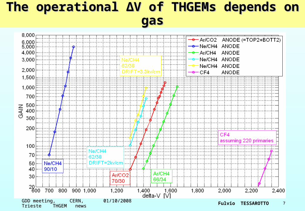
The operational The operational ΔΔVV of THGEMs depends of THGEMs depends on gason gas
Simulation performed using tools provided by RD51 Colleagues:
based on “ANSYS” and “GARFIELD”
Fulvio TESSAROTTO GDD meeting, CERN, 01/10/2008 Trieste THGEM newsGDD meeting, CERN, 01/10/2008 Trieste THGEM news 88
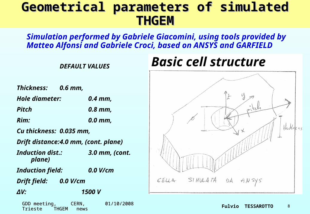
Geometrical parameters of simulated Geometrical parameters of simulated THGEMTHGEM
DEFAULT VALUES
Thickness: 0.6 mm,
Hole diameter: 0.4 mm,
Pitch 0.8 mm,
Rim: 0.0 mm,
Cu thickness: 0.035 mm,
Drift distance:4.0 mm, (cont. plane)
Induction dist.: 3.0 mm, (cont. plane)
Induction field: 0.0 V/cm
Drift field: 0.0 V/cm
ΔV: 1500 V
Basic cell structure
Simulation performed by Gabriele Giacomini, using tools provided by Matteo Alfonsi and Gabriele Croci, based on ANSYS and GARFIELD

Fulvio TESSAROTTO GDD meeting, CERN, 01/10/2008 Trieste THGEM newsGDD meeting, CERN, 01/10/2008 Trieste THGEM news 99
Values of Ez along the “z” axis, for different diameters
diameter scan
0
5000
10000
15000
20000
25000
30000
-0.1 -0.08 -0.06 -0.04 -0.02 0 0.02 0.04 0.06 0.08 0.1
z (cm)
Ez
(V/c
m)
0.1 mm
0.2
0.3
0.4
0.5
0.6
holescan along the
“z” axis (hole axis)
Thickness: 0.6 mm,
Pitch: 0.8 mm,
Induction field: 0.0 V/cm
Drift field: 0.0 V/cm
Fulvio TESSAROTTO GDD meeting, CERN, 01/10/2008 Trieste THGEM newsGDD meeting, CERN, 01/10/2008 Trieste THGEM news 1010
diameter scan
-10000
-7500
-5000
-2500
0
2500
5000
7500
10000
0 0.01 0.02 0.03 0.04 0.05 0.06 0.07
y (cm)
Ez
(V/c
m)
0.1 mm
0.2
0.3
0.4
0.5
0.6
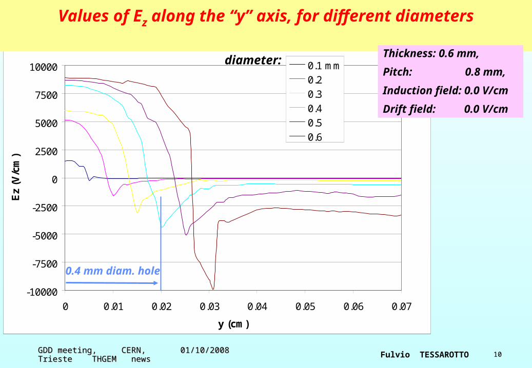
Values of Ez along the “y” axis, for different diameters
0.4 mm diam. hole
Thickness: 0.6 mm,
Pitch: 0.8 mm,
Induction field: 0.0 V/cm
Drift field: 0.0 V/cm
diameter:
Fulvio TESSAROTTO GDD meeting, CERN, 01/10/2008 Trieste THGEM newsGDD meeting, CERN, 01/10/2008 Trieste THGEM news 1111
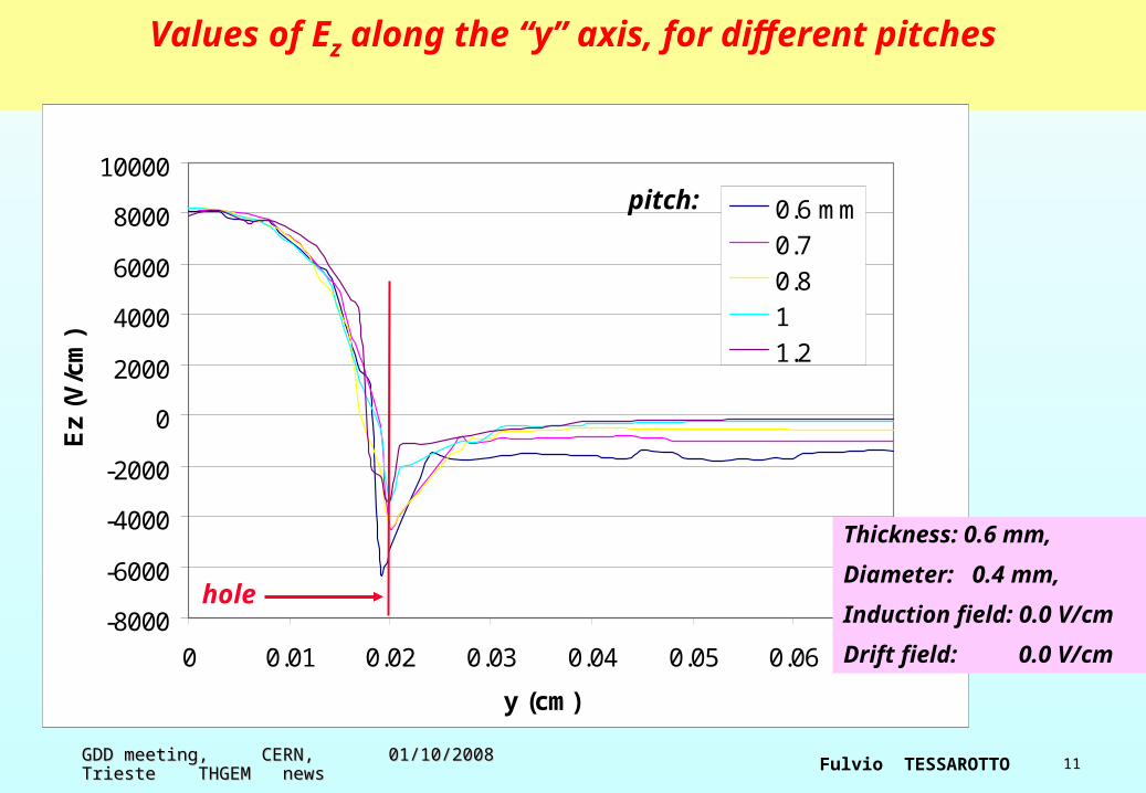
Values of Ez along the “y” axis, for different pitches
-8000
-6000
-4000
-2000
0
2000
4000
6000
8000
10000
0 0.01 0.02 0.03 0.04 0.05 0.06 0.07
y (cm)
Ez
(V/c
m)
0.6 mm
0.7
0.8
1
1.2
pitch:
hole
Thickness: 0.6 mm,
Diameter: 0.4 mm,
Induction field: 0.0 V/cm
Drift field: 0.0 V/cm
Fulvio TESSAROTTO GDD meeting, CERN, 01/10/2008 Trieste THGEM newsGDD meeting, CERN, 01/10/2008 Trieste THGEM news 1212
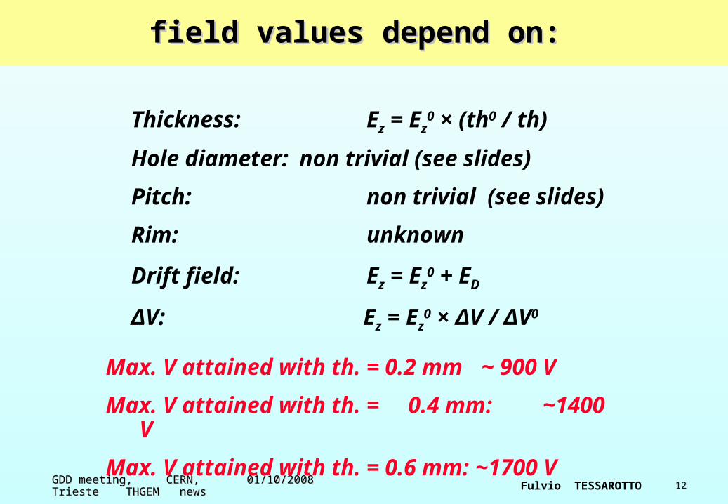
field values depend on: field values depend on:
Thickness: Ez = Ez0 × (th0 / th)
Hole diameter: non trivial (see slides)
Pitch: non trivial (see slides)
Rim: unknown
Drift field: Ez = Ez0 + ED
ΔV: Ez = Ez0 × ΔV / ΔV0
Max. V attained with th. = 0.2 mm ~ 900 V
Max. V attained with th. = 0.4 mm: ~1400 V
Max. V attained with th. = 0.6 mm: ~1700 V
Fulvio TESSAROTTO GDD meeting, CERN, 01/10/2008 Trieste THGEM newsGDD meeting, CERN, 01/10/2008 Trieste THGEM news 1313
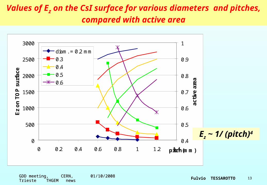
Values of Ez on the CsI surface for various diameters and pitches, compared with active area
0
500
1000
1500
2000
2500
3000
0 0.2 0.4 0.6 0.8 1 1.2 1.4pitch(mm)
Ez
on
TO
P s
urf
ace
0.4
0.5
0.6
0.7
0.8
0.9
1
acti
ve a
rea
diam. = 0.2 mm
0.3
0.4
0.5
0.6
Ez ~ 1/ (pitch)4
Fulvio TESSAROTTO GDD meeting, CERN, 01/10/2008 Trieste THGEM newsGDD meeting, CERN, 01/10/2008 Trieste THGEM news 1414
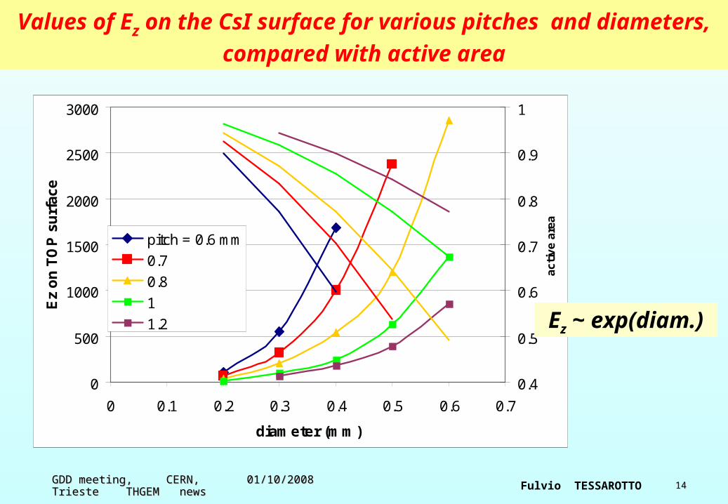
Values of Ez on the CsI surface for various pitches and diameters, compared with active area
0
500
1000
1500
2000
2500
3000
0 0.1 0.2 0.3 0.4 0.5 0.6 0.7
diameter (mm)
Ez
on
TO
P s
urf
ace
0.4
0.5
0.6
0.7
0.8
0.9
1
ac
tiv
e a
rea
pitch = 0.6 mm
0.7
0.8
1
1.2 Ez ~ exp(diam.)
Fulvio TESSAROTTO GDD meeting, CERN, 01/10/2008 Trieste THGEM newsGDD meeting, CERN, 01/10/2008 Trieste THGEM news 1515
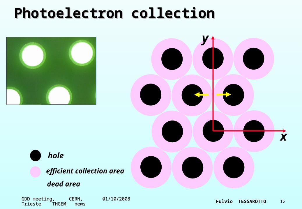
Photoelectron collectionPhotoelectron collection
hole
efficient collection area
dead area
x
y

Fulvio TESSAROTTO GDD meeting, CERN, 01/10/2008 Trieste THGEM newsGDD meeting, CERN, 01/10/2008 Trieste THGEM news 1616
trajectories for drift = 0 V/cm
x
y scan along the “y” axis
scan along the “x” axis
x
y
Collection efficiency is o.k.
y0- 0.2 0.2 0.5- 0.5
Ez = - 543 V/cm
th. 0.6 mm, diam. 0.4 mm, pitch: 0.8 mm, ΔV = 1500 V

Fulvio TESSAROTTO GDD meeting, CERN, 01/10/2008 Trieste THGEM newsGDD meeting, CERN, 01/10/2008 Trieste THGEM news 1717
trajectories for drift = -50 V/cm
x
y scan along the “y” axis
scan along the “x” axis
x
y
partial collection efficiency
y0- 0.2 0.2 0.5- 0.5
Ez = - 593 V/cm
“full collection radius” = 0.42 mm
th. 0.6 mm, diam. 0.4 mm, pitch: 0.8 mm, ΔV = 1500 V
Fulvio TESSAROTTO GDD meeting, CERN, 01/10/2008 Trieste THGEM newsGDD meeting, CERN, 01/10/2008 Trieste THGEM news 1818
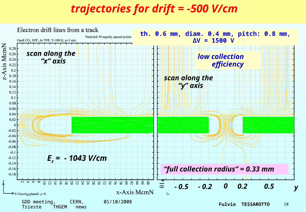
trajectories for drift = -500 V/cm
scan along the “y” axis
scan along the “x” axis
low collection efficiency
y0- 0.2 0.2 0.5- 0.5
Ez = - 1043 V/cm“full collection radius” = 0.33 mm
th. 0.6 mm, diam. 0.4 mm, pitch: 0.8 mm, ΔV = 1500 V

Fulvio TESSAROTTO GDD meeting, CERN, 01/10/2008 Trieste THGEM newsGDD meeting, CERN, 01/10/2008 Trieste THGEM news 1919
trajectories for drift = +500 V/cm
scan along the “y” axis
scan along the “x” axis
Ez by far too low
y0- 0.2 0.2 0.5- 0.5
Ez = - 43 V/cm x
yy
x
th. 0.6 mm, diam. 0.4 mm, pitch: 0.8 mm, ΔV = 1500 V
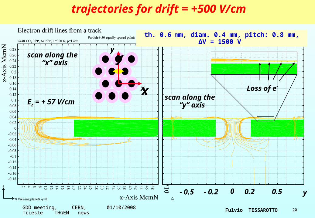
Fulvio TESSAROTTO GDD meeting, CERN, 01/10/2008 Trieste THGEM newsGDD meeting, CERN, 01/10/2008 Trieste THGEM news 2020
trajectories for drift = +500 V/cm
scan along the “y” axis
scan along the “x” axis
y0- 0.2 0.2 0.5- 0.5
Ez = + 57 V/cmx
yy
x Loss of e-
th. 0.6 mm, diam. 0.4 mm, pitch: 0.8 mm, ΔV = 1500 V

Fulvio TESSAROTTO GDD meeting, CERN, 01/10/2008 Trieste THGEM newsGDD meeting, CERN, 01/10/2008 Trieste THGEM news 2121
Consistency check with other Consistency check with other simulation programssimulation programs
lattice spacing:
50 μm, 30 μm, 20 μm

Fulvio TESSAROTTO GDD meeting, CERN, 01/10/2008 Trieste THGEM newsGDD meeting, CERN, 01/10/2008 Trieste THGEM news 2222
Consistency check with other Consistency check with other simulation programssimulation programs
diameter scan
-10000
-7500
-5000
-2500
0
2500
5000
7500
10000
0 0.01 0.02 0.03 0.04 0.05 0.06 0.07
y (cm)
Ez
(V/c
m)
0.1 mm0.20.30.40.50.6
Fulvio TESSAROTTO GDD meeting, CERN, 01/10/2008 Trieste THGEM newsGDD meeting, CERN, 01/10/2008 Trieste THGEM news 2323
Main uses of UV lightMain uses of UV light
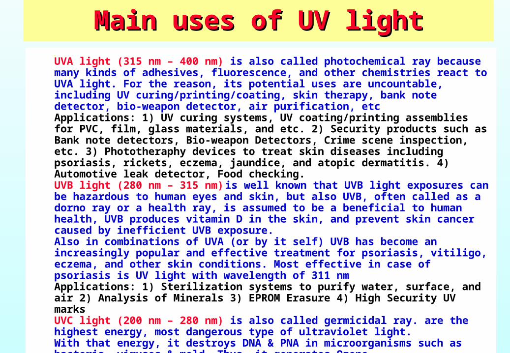
UVA light (315 nm – 400 nm) is also called photochemical ray because many kinds of adhesives, fluorescence, and other chemistries react to UVA light. For the reason, its potential uses are uncountable, including UV curing/printing/coating, skin therapy, bank note detector, bio-weapon detector, air purification, etc Applications: 1) UV curing systems, UV coating/printing assemblies for PVC, film, glass materials, and etc. 2) Security products such as Bank note detectors, Bio-weapon Detectors, Crime scene inspection, etc. 3) Phototheraphy devices to treat skin diseases including psoriasis, rickets, eczema, jaundice, and atopic dermatitis. 4) Automotive leak detector, Food checking. UVB light (280 nm – 315 nm) is well known that UVB light exposures can be hazardous to human eyes and skin, but also UVB, often called as a dorno ray or a health ray, is assumed to be a beneficial to human health, UVB produces vitamin D in the skin, and prevent skin cancer caused by inefficient UVB exposure.Also in combinations of UVA (or by it self) UVB has become an increasingly popular and effective treatment for psoriasis, vitiligo, eczema, and other skin conditions. Most effective in case of psoriasis is UV light with wavelength of 311 nmApplications: 1) Sterilization systems to purify water, surface, and air 2) Analysis of Minerals 3) EPROM Erasure 4) High Security UV marks UVC light (200 nm – 280 nm) is also called germicidal ray. are the highest energy, most dangerous type of ultraviolet light. With that energy, it destroys DNA & PNA in microorganisms such as bacteria, viruses & mold, Thus, it generates Ozone.Especially 254.7nm is most effective wavelength for disinfectionsApplications: 1) Water/Surface purification system 2) Laboratory testing devices

Fulvio TESSAROTTO GDD meeting, CERN, 01/10/2008 Trieste THGEM newsGDD meeting, CERN, 01/10/2008 Trieste THGEM news 2424
LED at 255 nmLED at 255 nm


![Thick GEM versus thin GEM in two-phase argon avalanche ... · presented elsewhere [15,16,18,28]. Here we describe details relevant to THGEM performance in general and to THGEM and](https://static.fdocuments.net/doc/165x107/601aa2bd1fb51279164b0325/thick-gem-versus-thin-gem-in-two-phase-argon-avalanche-presented-elsewhere-15161828.jpg)


