
1 Enabling Technologies for the Mass Storage Industry Dr. David Tuckerman, CTO...
14
Transcript of 1 Enabling Technologies for the Mass Storage Industry Dr. David Tuckerman, CTO...

2
Enabling Technologies for Data Storage
Semiconductor evolving to ever-smaller devicesFeature size going down, currently 65 nmDie Thickness below 100 micronReduced voltages and power needs
Advanced Packaging keeps finished ICs smallChip Scale Packaging, final footprint is die-sizeBall Grid Arrays attach directly to PCB without leadsStacked and Folded Packages
“Systems in a Package” DesignsDifferent functions combined at die levelOne chip does the work of many dieComplete function in a single package (GPS, cellular, imaging)
3
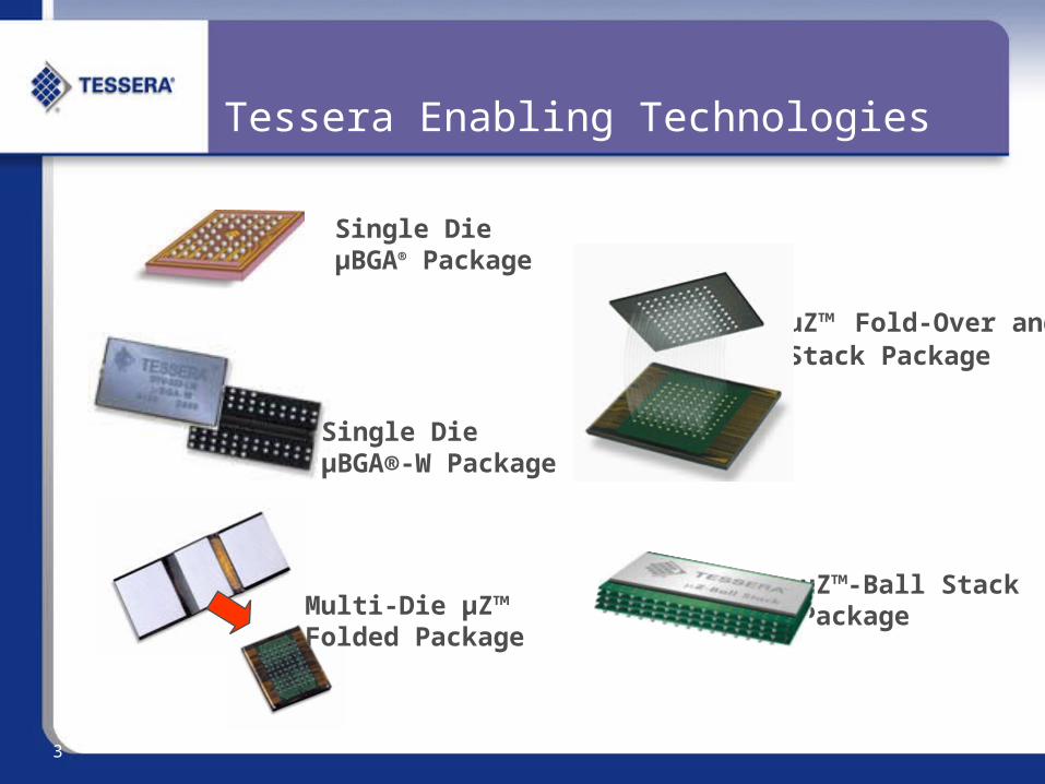
Tessera Enabling Technologies
µZ™-Ball Stack Package
Single Die µBGA®-W Package
Multi-Die µZ™ Folded Package
µZ™ Fold-Over and Stack Package
Single Die µBGA® Package
4
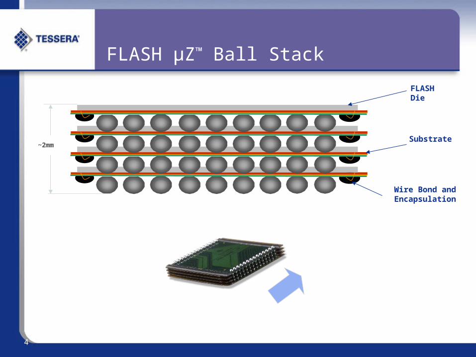
FLASH µZ™ Ball Stack
FLASH Die
Substrate
Wire Bond and Encapsulation
~2mm
5
µZ™ - Ball Stack Package
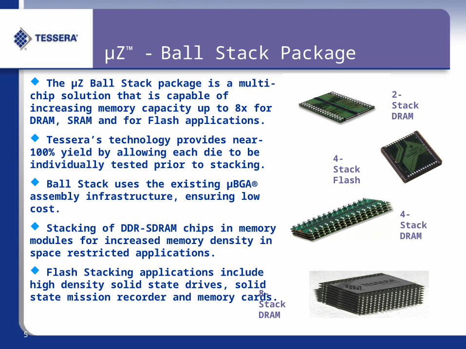
The µZ Ball Stack package is a multi-chip solution that is capable of increasing memory capacity up to 8x for DRAM, SRAM and for Flash applications.
Tessera’s technology provides near-100% yield by allowing each die to be individually tested prior to stacking.
Ball Stack uses the existing µBGA® assembly infrastructure, ensuring low cost.
Stacking of DDR-SDRAM chips in memory modules for increased memory density in space restricted applications.
Flash Stacking applications include high density solid state drives, solid state mission recorder and memory cards.
2-Stack DRAM
4-Stack Flash
4-Stack DRAM
8-Stack DRAM

6
Small Device Applications
Cellular PhonesIntel pioneered stacked memory in hand-held devicesFeatures added while shrinking overall phone dimensionsNew features require more memoryFederal mandate requires GPS receivers on new cellular phones
PC and Server MemoryBlade servers and laptops are severely space constrainedDie stacking allows 8X the device count in same footprintFewer leads, simpler PCB
Military and Aerospace“Land Warrior” requires ultra small “wearable” computerDevices must work in hostile environments (high G, vacuum)High reliability, low power, “survivability” are key issues
7
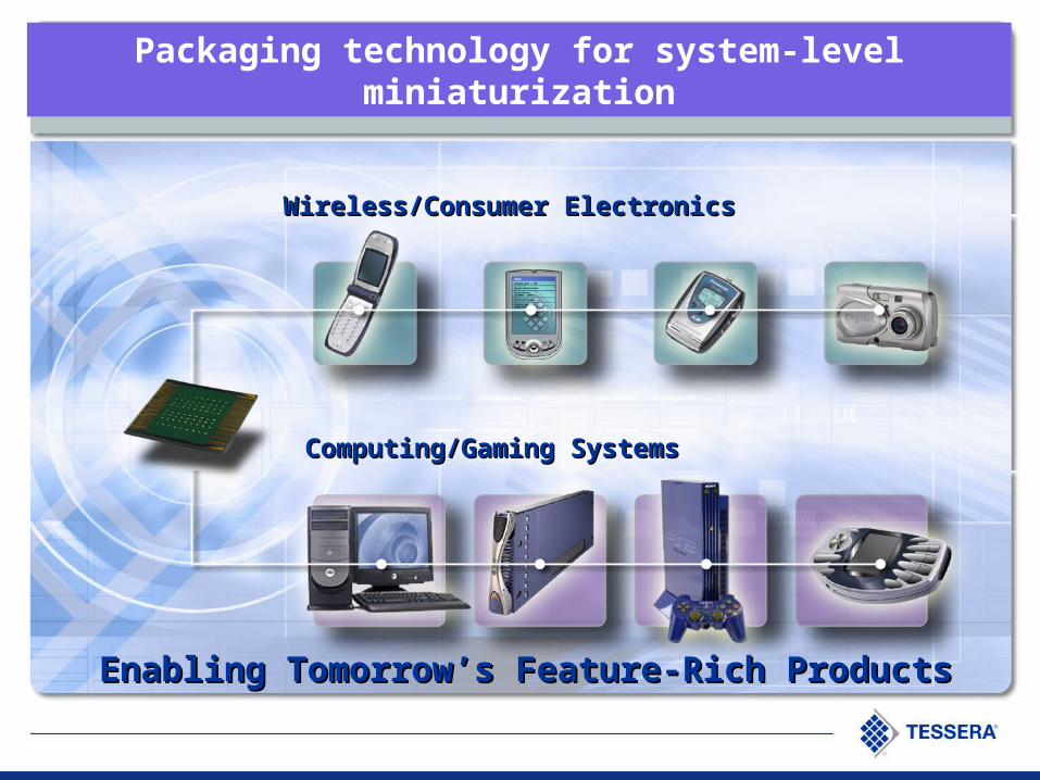
Computing/Gaming SystemsComputing/Gaming Systems
Wireless/Consumer ElectronicsWireless/Consumer Electronics
Enabling Tomorrow’s Feature-Rich ProductsEnabling Tomorrow’s Feature-Rich Products
Packaging technology for system-level miniaturization
8
Typical Applications
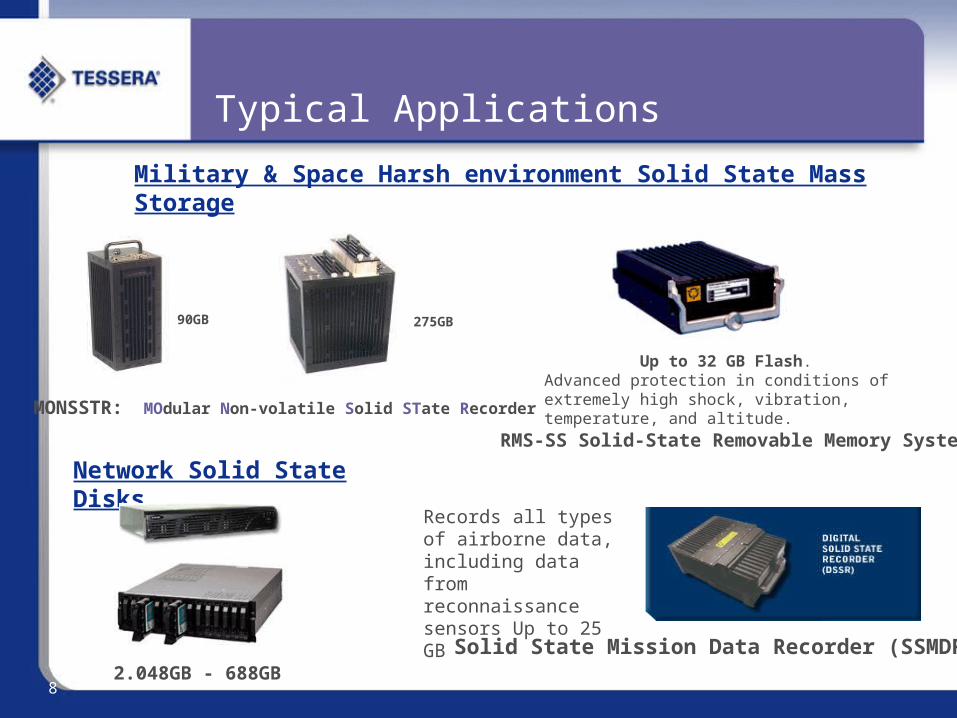
MONSSTR: MOdular Non-volatile Solid STate Recorder
Military & Space Harsh environment Solid State Mass Storage
90GB 275GB
Up to 32 GB Flash.Advanced protection in conditions of extremely high shock, vibration, temperature, and altitude.
RMS-SS Solid-State Removable Memory System
Solid State Mission Data Recorder (SSMDR)
Records all types of airborne data, including data from reconnaissance sensors Up to 25 GB
Network Solid State Disks
2.048GB - 688GB
9
Solid State Drive Application
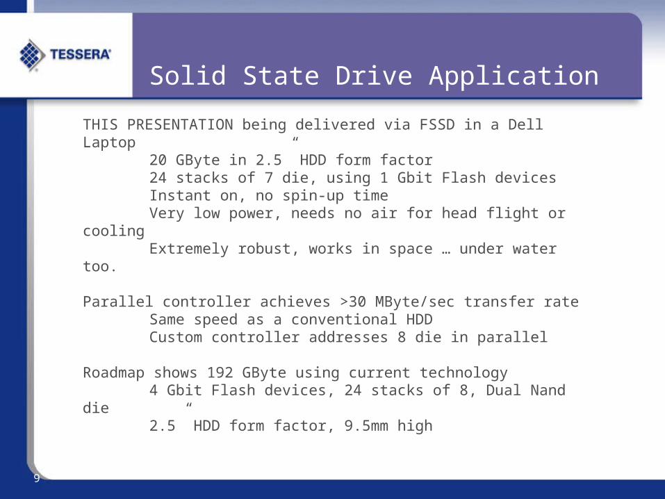
THIS PRESENTATION being delivered via FSSD in a Dell Laptop20 GByte in 2.5” HDD form factor24 stacks of 7 die, using 1 Gbit Flash devicesInstant on, no spin-up timeVery low power, needs no air for head flight or coolingExtremely robust, works in space … under water too.
Parallel controller achieves >30 MByte/sec transfer rateSame speed as a conventional HDDCustom controller addresses 8 die in parallel
Roadmap shows 192 GByte using current technology 4 Gbit Flash devices, 24 stacks of 8, Dual Nand die2.5” HDD form factor, 9.5mm high
10
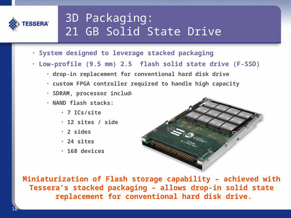
3D Packaging:21 GB Solid State Drive
• System designed to leverage stacked packaging
• Low-profile (9.5 mm) 2.5” flash solid state drive (F-SSD)
• drop-in replacement for conventional hard disk drive
• custom FPGA controller required to handle high capacity
• SDRAM, processor included
• NAND flash stacks:
• 7 ICs/site
• 12 sites / side
• 2 sides
• 24 sites
• 168 devices
Miniaturization of Flash storage capability – achieved with Tessera’s stacked packaging – allows drop-in solid state
replacement for conventional hard disk drive.
11
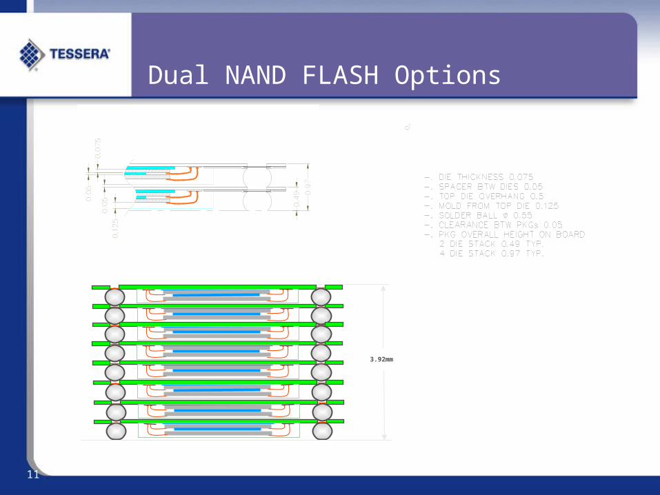
Dual NAND FLASH Options
3.92mm
12
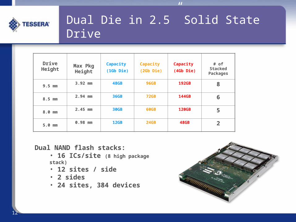
Dual Die in 2.5” Solid State Drive
Drive Height
Max Pkg Height
Capacity
(1Gb Die)
Capacity
(2Gb Die)
Capacity
(4Gb Die)
# of Stacked Packages
9.5 mm3.92 mm 48GB 96GB 192GB 8
8.5 mm2.94 mm 36GB 72GB 144GB 6
8.0 mm2.45 mm 30GB 60GB 120GB 5
5.0 mm0.98 mm 12GB 24GB 48GB 2
Dual NAND flash stacks:• 16 ICs/site (8 high package stack)
• 12 sites / side• 2 sides • 24 sites, 384 devices
13
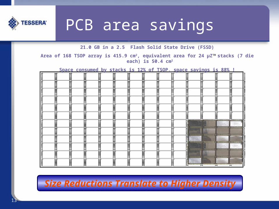
PCB area savings
Size Reductions Translate to Higher Density
21.0 GB in a 2.5” Flash Solid State Drive (FSSD)
Area of 168 TSOP array is 415.9 cm2, equivalent area for 24 µZTM stacks (7 die each) is 50.4 cm2
Space consumed by stacks is 12% of TSOP, space savings is 88% !

14
Summary and Conclusions
Semiconductor Packaging a key element for solid state memory productsHigher frequencies need shortest possible connections“System in a Package” simplifies PCB, improves reliabilityMemory demand growth requires die stacking
Today’s “nice to have” will be tomorrow’s “must have” featuresDDR-2 requires Chip Scale Packaging, so will DDR-3More products must be tolerant of hostile environmentsAdditional space savings from Integrated passives
More products will depend on miniature and/or hand-held form factorsMilitary devices carried by personnel and ordnanceBusiness needs for tracking people, equipment, products (RFID)Consumer goods, increasing use of wired/wireless networks