1 DESIGN OF 8-BIT ALU Vijigish Lella Harish Gogineni Bangar Raju Singaraju Advisor: Dr. David W....
20
1 DESIGN OF 8-BIT ALU Vijigish Lella Harish Gogineni Bangar Raju Singaraju Advisor: Dr. David W. Parent 8 May 2006
-
date post
21-Dec-2015 -
Category
Documents
-
view
222 -
download
2
Transcript of 1 DESIGN OF 8-BIT ALU Vijigish Lella Harish Gogineni Bangar Raju Singaraju Advisor: Dr. David W....

1
DESIGN OF 8-BIT ALU
Vijigish LellaHarish Gogineni
Bangar Raju Singaraju
Advisor: Dr. David W. Parent8 May 2006

2
Agenda
• Abstract• Introduction• Summary of Results• Project (Experimental) Details• Results• Conclusions

3
Abstract
• The Aim of the project is to design a 8-bit ALU.
• The circuit is designed so as to meet the following specifications: – Frequency: 200 MHz.– Power : 100 mW. – Area : 576x840 µm2
• The design was done in AMI06 technology using Cadence tools.

4
Introduction
Why this project?
• The ALU is a fundamental building block of any computing system.
• Challenging to design a 18 logic level design using CMOS Technology.
• Design consists of different kinds of logic… Brent-Kung Adder, DFF, AOI3333, Mux, Inv, Nand, Nor, Xor, etc.

5
Design Flow
Selection of Adder
Timing and PowerAnalysis
Calculations for the
Critical Path
Gate level Design
Functional Table
NC VerilogVerification
DRC & LVS for each bit
Layout of Individual cells
Schematic of Individual cells
Final DRC & LVS
Integration of bits

6
Project Summary
• The ALU performs 1 Arithmetic function and 9 Logical functions at 200MHz.
• Uses Brent Kung Adder to perform addition.
• Design uses maximum power of 100mW
• Maximum area is 576 x 840µm2

7

8

9
Schematic

10
0 1 1 0 0 0 0 1
0 1 1 0 0 0 0 0
0 0 0 1 0 0 0 0
0 1 1 1 0 0 0 0
1 1 0 0 0 0 0 0
1 1 1 0 0 0 0 0
0 0 0 0 0 0 0 0
0 1 1 1 0 0 0 0
1 0 0 0 0 0 0 0
1 0 0 1 0 0 0 0
ADD
AxorB
AB
A+B
AINV
BINV
Generate
C1 C2 C3 C4 C5 C6 C7 C8
Propagate
NAND
M
OR
NOR
XNOR

11
Longest Path Calculations
Total Propagation delay for the longest path = 3.72ns
INV
AOI22
INV
AOI22
XOR2
INV
INV
AOI21
INV
NAND2
INV
NAND2
INV
NAND2
INV
NAND2
INV
AOI3333
1.90E-15
1.90E-15
1.90E-15
2.60E-15
2.70E-15
2.70E-15
3.50E-15
3.60E-15
4.00E-15
4.50E-15
5.50E-15
6.00E-15
6.50E-15
1.05E-14
1.10E-14
1.65E-14
1.70E-14
2.00E-14
2.0000E-14
2.1026E-14
2.2390E-14
4.6206E-14
4.2092E-14
2.2826E-14
4.2877E-14
2.4171E-14
3.9861E-14
2.2583E-14
4.7082E-14
4.1353E-14
5.7941E-14
4.5035E-14
5.6127E-14
4.6848E-14
5.7171E-14
4.2571E-14
7.00E-11
2.80E-10
7.00E-11
3.50E-10
3.30E-10
7.50E-11
9.90E-11
2.50E-10
1.00E-10
1.20E-10
1.20E-10
1.40E-10
1.30E-10
1.55E-10
1.30E-10
1.65E-10
1.50E-10
9.90E-10
1 1 1 1 1.813
2 2 3 4 1.760
1 1 1 1 1.813
2 2 3 4 1.743
2 2 3 4 1.748
1 1 1 1 1.811
1 1 1 1 1.805
2 2 2 3 1.768
1 1 1 1 1.805
2 1 2 1 0.900
1 1 1 1 1.800
2 1 2 1 0.898
1 1 1 1 1.798
2 1 2 1 0.896
1 1 1 1 1.798
2 1 2 1 0.894
1 1 1 1 1.793
1.583
4.45E-04 8.07E-04
4.83E-04 8.51E-04
4.89E-04 8.87E-04
4.57E-04 7.97E-04
4.95E-04 8.65E-04
4.54E-04 8.23E-04
5.13E-04 9.27E-04
4.29E-04 7.58E-04
4.80E-04 8.66E-04
7.38E-04 6.64E-04
4.40E-04 7.92E-04
9.10E-04 8.17E-04
4.80E-04 8.62E-04
8.82E-04 7.90E-04
4.99E-04 8.97E-04
8.99E-04 8.04E-04
4.54E-04 8.14E-04
6.12E-04 9.69E-04
GATE C int Cg Tphl Nsn Nsp N M R Wn WpF F s cm cm

12
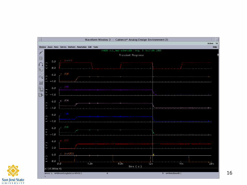
Simulation (Arithmetic operations)

13
Layout
DF
FIN
PU
T OU
TP
UT

14
Verification

15
16

17
Results
• The ALU performs all 10 functions at a 200MHz clock and a load of 20fF.
• Area of the layout is 576 x 840µm2

18
Conclusions
• Designed a 8-Bit ALU that performs arithmetic and logical functions at 200MHz frequency driving up to 20fF.
• The Logic design can be modified to perform more functions.

19
Lessons Learned
• Cell based design• Uniform cell height• Floor planning• Grid pattern for Vdd and gnd• Debugging LVS errors using extracted view

20
Acknowledgements
• Thanks to Professor David W. Parent for his guidance.
• Thanks to Cadence Design Systems for the VLSI lab