1 Chapter 4 Circuit characterization and Performance Estimation.
48
1 Chapter 4 Circuit characterization and Performance Estimation
-
Upload
blanche-brown -
Category
Documents
-
view
259 -
download
4
Transcript of 1 Chapter 4 Circuit characterization and Performance Estimation.
1
Chapter 4
Circuit characterization and Performance Estimation

2
Introduction
Need simple models to estimate system performance in terms of signal delay and power dissipation.
Each layer in an MOS transistor has both resistance and capacitance that are fundamental components in estimating the performance of a circuit or system.
They also have inductance characteristics that is assumed to be negligible.

3
Introduction
• Issues include: Resistance, capacitance and inductance calculations. Delay estimations. Determination of conductor size for power and clock
distribution. Power consumption. Charge sharing mechanisms. Design Margining. Reliability. Effects of scaling.

4
Resistance Estimation
s( ) (ohms) where R sheet resistance=Rs
lR R
w
( )( ) where =resistivity, t=thickness, =length/widthl l
Rt w w
The resistance of a uniform slab of conducting material may be expressed as:
Alternatively as
l
w
t
1 Rectangular BlockR = R (L/W)
4 Rectangular BlocksR = R (2L/2W) = R (L/W)
t
l
w w
l

5
Choice of Metals• Until 180 nm generation, most wires were aluminum• Modern processes often use copper
– Cu atoms diffuse into silicon and damage FETs– Must be surrounded by a diffusion barrier
Metal Bulk resistivity (*cm)
Silver (Ag) 1.6
Copper (Cu) 1.7
Gold (Au) 2.2
Aluminum (Al) 2.8
Tungsten (W) 5.3
Molybdenum (Mo) 5.3

6
Sheet Resistance
Typical sheet resistance values for materials are very well characterized
Layer Rs (Ohm / Sq)
Aluminium 0.03
N Diffusion 10 – 50
Silicide 2 – 4
Polysilicon 15 - 100
N-transistor Channel 104
P-transistor Channel 2.5 x 10⁴
Typical Sheet Resistances for 5µm Technology

7
Sheet ResistanceNote: L defined parallel to current and W defined perpendicular to current.

8
Sheet Resistance

9
Rs for poly is 4 /square in 1micron tech.
Rpoly = 4 /square x (19/3 + 11/4 + 19/3) squares = 61.6 .
A note: A corner square has a sheet resistance of ~0.5 Rs.

10
Corner (1/2 Square)
Corner (1/2 Square)1/2 Square
Corner (1/2 Square)
1/2 Square
Example:R = Rs(poly) * 13 + 2*(1/2) + 3*(1/2) squaresR = 4Ω/sq * 15.5 squares = 62Ω
Example

11
Resistance Estimation
Channel resistance can be estimated in the linear region as:
1 1
( ) ( )cox GS t GS t
LR ohms
C V V W K V V
A range of 1,000 to 30,000 ohms/square are possible for n-channel and p-channel devices.
Temperature changes both (mobility) and Vt (threshold voltage) and therefore channel resistance.Channel resistance increases with temperature, approximately +0.25% per degree C above 25 degrees.Metal and poly resistance change about 0.3% and well diffusions about 1% per degree C.

12
Capacitance Estimation
Switching speed of MOS systems strongly dependent: Parasitic capacitances associated with the MOS transistor. Interconnect capacitance of "wires". Resistance of transistors and wires.
Total load capacitance on the output of a CMOS gate is sum of: Gate capacitance (of receiver logic gates downstream). Driver diffusion (source/drain) capacitance. Routing ( line ) capacitance of substrate and other wires.
13
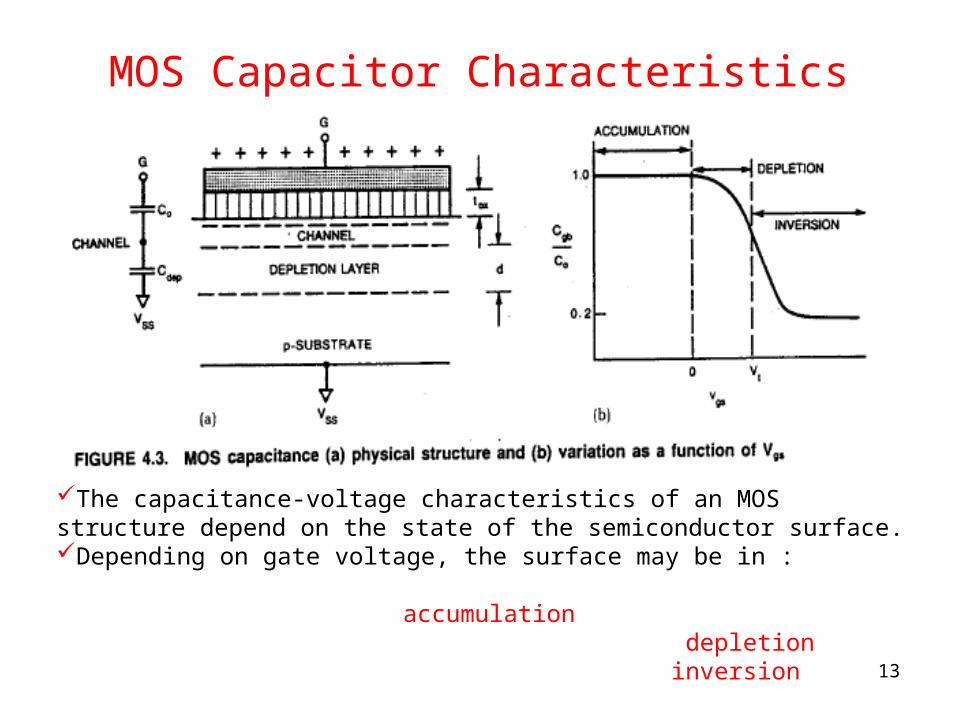
MOS Capacitor Characteristics
The capacitance-voltage characteristics of an MOS structure depend on the state of the semiconductor surface.Depending on gate voltage, the surface may be in :
accumulation depletion
inversion

14
MOS Capacitor Characteristics
In accumulation:
In deletion mode
15
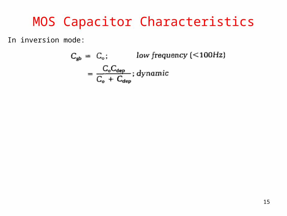
MOS Capacitor CharacteristicsIn inversion mode:
16
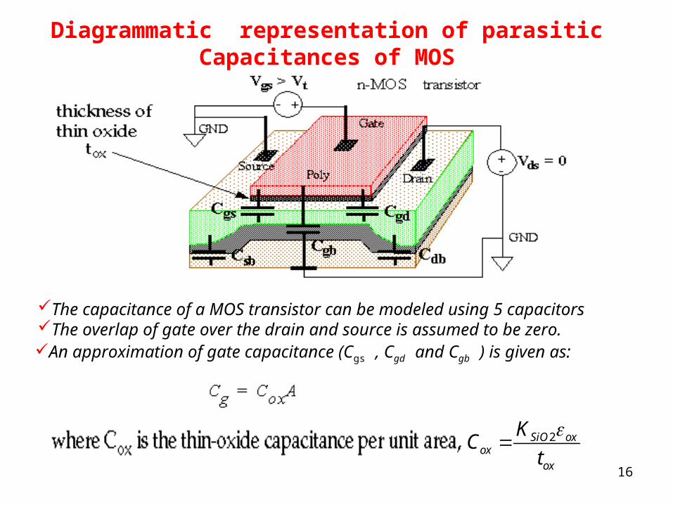
Diagrammatic representation of parasitic Capacitances of MOS
The capacitance of a MOS transistor can be modeled using 5 capacitorsThe overlap of gate over the drain and source is assumed to be zero. An approximation of gate capacitance (Cgs , Cgd and Cgb ) is given as:
2SiO oxox
ox
KC
t

17
Estimating Gate CapacitanceFor example, for thin-oxide thickness of 15 nm
In = 0.5 technology, W = 2 and L = 1
This is a conservative estimate of gate capacitance that does not include fringing fields (extrinsic) gate capacitance.
Gate capacitance increases as the thin-oxide thins.

18
The total gate Capacitance
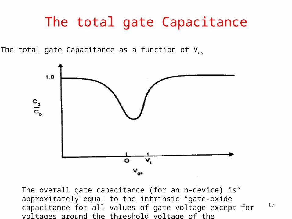
19
The total gate Capacitance
The total gate Capacitance as a function of Vgs
The overall gate capacitance (for an n-device) is approximately equal to the intrinsic “gate-oxide” capacitance for all values of gate voltage except for voltages around the threshold voltage of the transistor, Vt
20
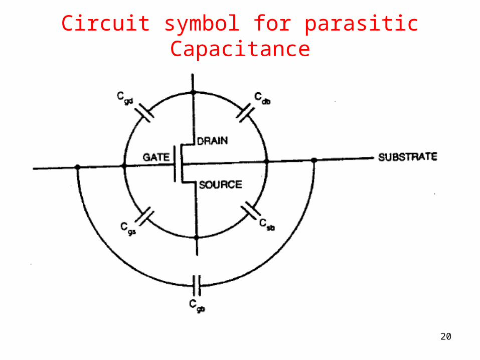
Circuit symbol for parasitic Capacitance

21
Estimating Source/Drain Capacitance
This model assumes a zero DC bias across the junction.

22
Estimating Source/Drain Capacitance

23
Estimating Source/Drain CapacitanceFor example:
Typical values for 0.5 micron process
n-channel device
Because of fan-out, gate capacitance usually dominates the loading.

24
Estimating Routing CapacitanceRouting capacitance between metal and poly can be approximated using aparallel-plate model.
The parallel-plate model approximation ignores fringing fields.The effect of the fringing fields is to increase the effective area of the plates.Consequently, poly and metal lines will actually have a higher capacitance than that predicted by the model.
As line widths are scaled, the width (w) and heights of wires tend to reduce less than their separations. Accordingly, this fringing effect increases in importance.

25
Estimating Routing Capacitance
C=Cplate*area+CFringe*peripheral
Example:
Poly: Cplate-poly*12*4+Cfringe-poly*2*(12+4)
Metal:Cplate-metal1*12*4+Cfringe-metal1*2*(12+4)

26
Estimating Capacitance
Example:
CPoly=2* (2 * 2 ) Cpoly (plate) + 2* (2 + 2 + 2) Cpoly (fringe)
Cg=4 * 2 Cox

27
Estimating CapacitanceExample:
Cنفوذ=[12 *3 + 4 *4 ]* Cنفوذ(plate) + (3 +12 + 1 + 4 + 16 ) * c نفوذ- جانبی
C 6=فلز * 10 * C(plate)+ 2*(6 + 10) * C (fringe)
Cکل = Cنفوذ + Cفلز
28
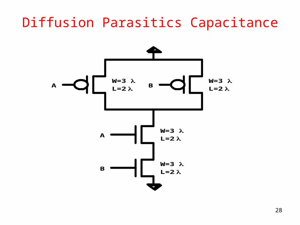
Diffusion Parasitics Capacitance
W=3 L=2 A B
W=3 L=2
A
B
W=3 L=2
W=3 L=2
29
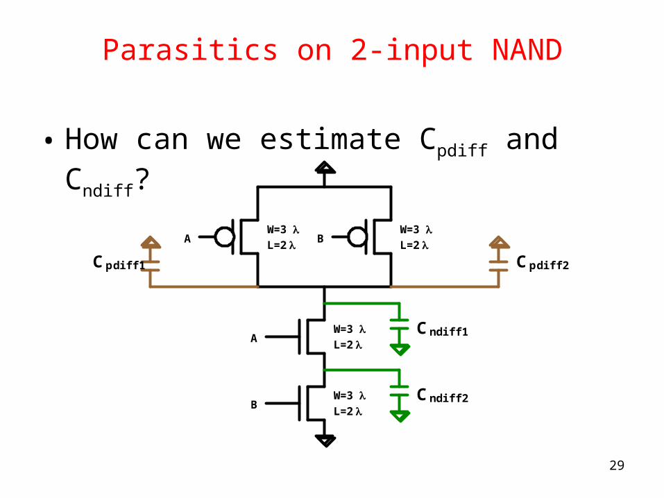
Parasitics on 2-input NAND
• How can we estimate Cpdiff and Cndiff?
W=3 L=2 A B
W=3 L=2
A
B
W=3 L=2
W=3 L=2
Cndiff2
Cpdiff2Cpdiff1
Cndiff1

30
NAND Layout
Cndiff 2 3 2 0.0625m / 2 0.6fF / m2
(3 2 3 2) 0.25m / 0.2fF /m
0.225fF 0.5fF 0.725fF
Cndiff1 (44 13)0.0625m / 2 0.6fF / m2
(5 4 4 1 1 3) 0.25m / 0.2fF / m
0.7125fF 0.9fF 1.625fF
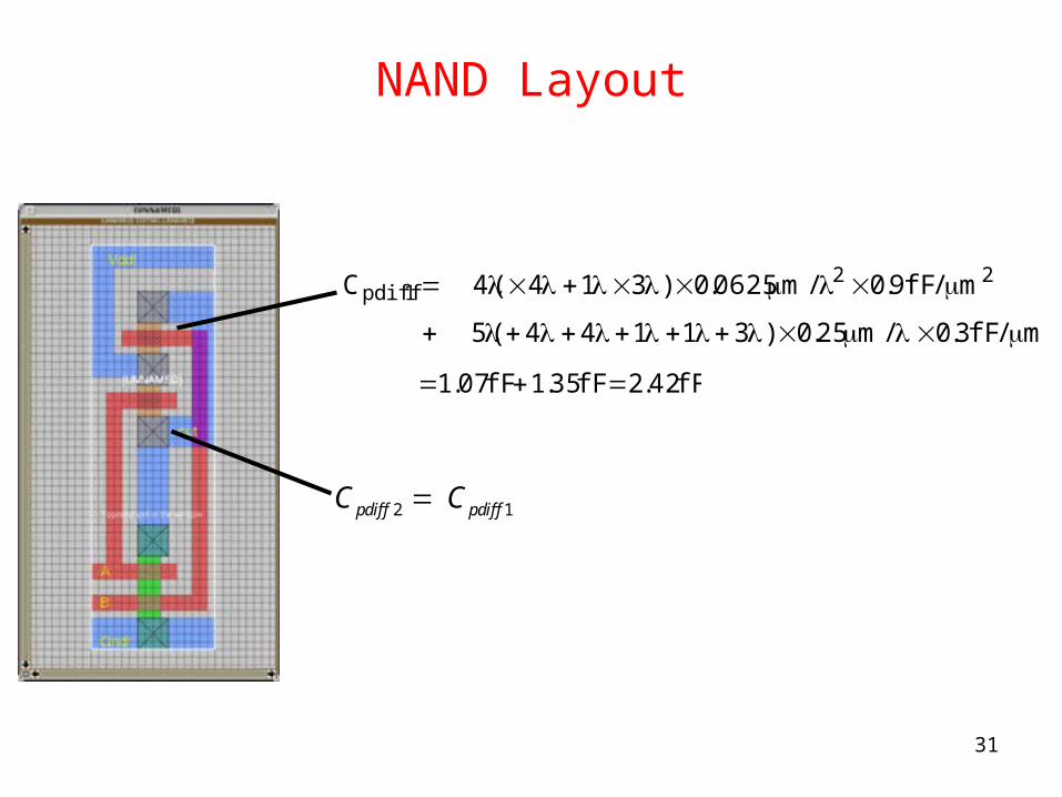
31
NAND Layout
2 1 pdiff pdiffC C
Cpdiff1 (44 13) 0.0625m / 2 0.9fF / m2
(5 4 4 1 1 3) 0.25m / 0.3fF / m
1.07fF 1.35fF 2.42fF

32
Diffusion Parasitics - Summing Up
W=3L=2A B
W=3L=2
A
B
W=3L=2
W=3L=2
Cndiff2
Cndiff1
+ Cpdiff1 + Cpdiff2
= 0.725fF
= 6.465fF

33
Delay in Long Wires - Lumped RC Model
• What is the delay in a long wire?
• Lumped RC Model:
• Delay time constant (ignoring driving gate) = R * C = (Rs * L / W) * (L * W * Cplate )
= r * c * L2
R = Rs * L / W = r*L(r = Rs / W - resistance per unit length )C = L * W * Cplate = c*L(c = W * Cplate - capacitance per unit length)
R C
in out
Linout

34
Wire Delay Models– Lumped RC Model
• Total wire resistance is lumped into a single R and total capacitance into a single C
• Good for short wires; pessimistic and inaccurate for long wires
Vout(t) = VDD(1-exp(-t/RC))
V50%(t) = VDD(1-exp(-PLH/RC))τPLH ≈ 0.69RC
R
C
VoutVin

35
Wire Delay ModelsT-Model
The above simple lumped RC model can be significantly improved by the T-model as
R/2
CVoutVin
R/2
model
This model is used in Elmore Model

36
Delay in Long Wires -Distributed RC Model
• Alternative: Break wire into small segments
• Approx. Solution - 1st moment of impulse response
• Important: delay still grows as square of length
R1 = rLin out
R2 = rL Rn = rL
Cn
cL
C2
cL
C1
cL
(Vout ) rc L 2 N N 1 2
(Vout ) rcL2
2 for N
37
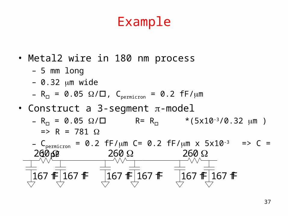
Example
• Metal2 wire in 180 nm process– 5 mm long– 0.32 m wide
– R = 0.05 /, Cpermicron = 0.2 fF/m
• Construct a 3-segment -model– R = 0.05 / R= R *(5x10⁻³/0.32 m ) => R = 781
– Cpermicron = 0.2 fF/m C= 0.2 fF/m x 5x10-3 => C = 1 pF
260
167 fF 167 fF
260
167 fF 167 fF
260
167 fF 167 fF
38

39

40

41
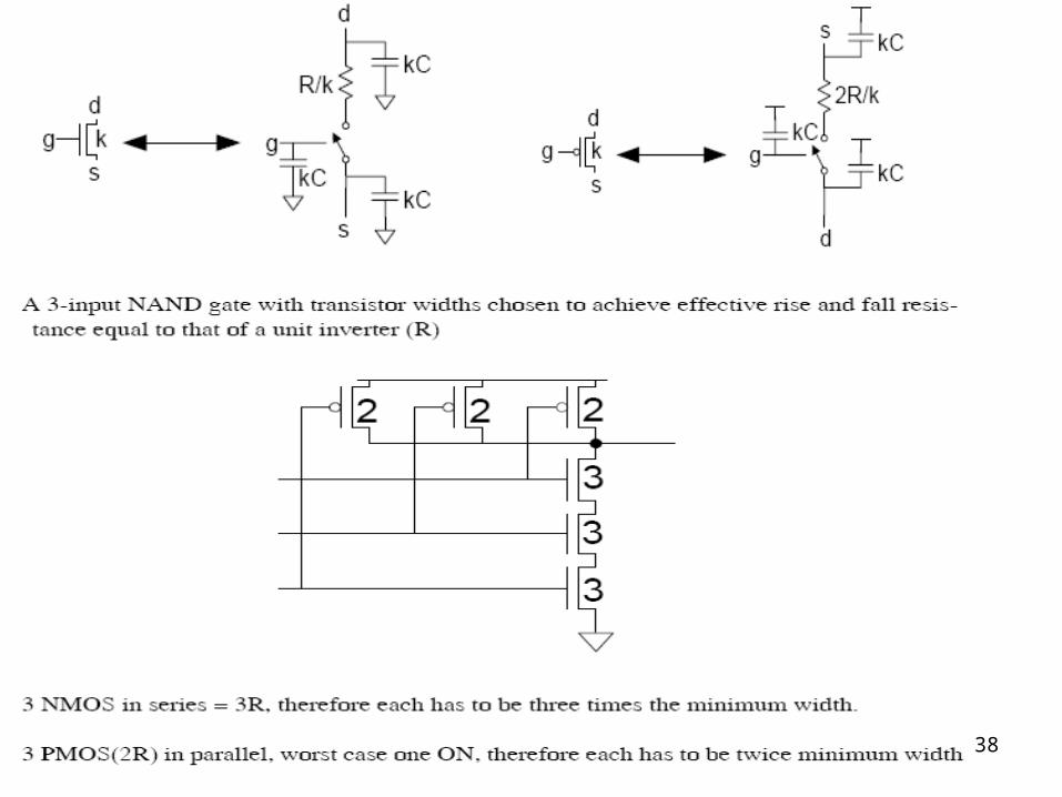
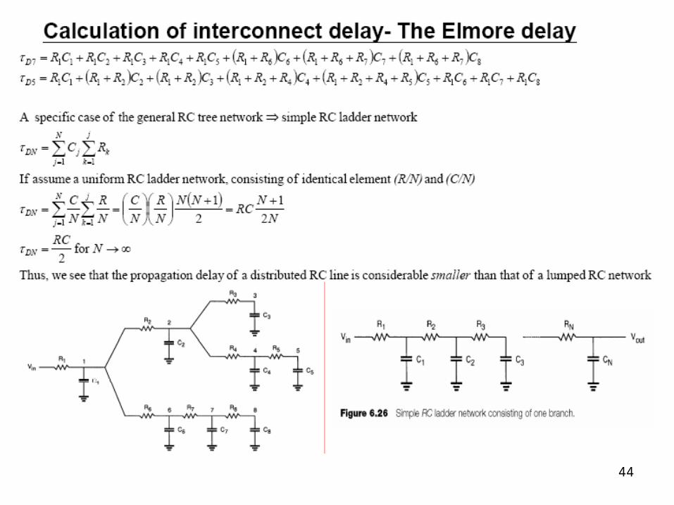
Elmore Delay Model

42
Elmore Delay
• ON transistors look like resistors• Pullup or pulldown network modeled as RC ladder• Elmore delay of RC ladder
R1 R2 R3 RN
C1 C2 C3 CN
nodes
1 1 1 2 2 1 2... ...
pd i to source ii
N N
t R C
RC R R C R R R C

43
The Elmore Delay Estimation Technique
MUX
srca
b
D5
D4
D2
tD4: delay from src to D4
tD5 ≠ tD4 ≠ tD2
src r1 r3
r5
r4
r2
C5
C4
C3
C2
C1
44

45
46
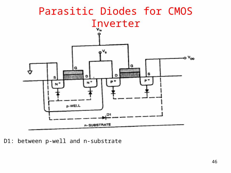
Parasitic Diodes for CMOS Inverter
D1: between p-well and n-substrate

47

48
Switching Power Dissipation of CMOS inverters
Vdsn Vdsp