1 2009 PROFIT The Changing Roles of Verification and Test in the Late-Silicon Era Tim Cheng...
29
1 2009 PROFIT The Changing Roles of Verification and Test in the Late-Silicon Era Tim Cheng University of California, Santa Barbara Sanya, China December 22, 2009
-
date post
19-Dec-2015 -
Category
Documents
-
view
217 -
download
3
Transcript of 1 2009 PROFIT The Changing Roles of Verification and Test in the Late-Silicon Era Tim Cheng...

1
2009 PROFIT
The Changing Roles of Verification and Test in the
Late-Silicon Era
Tim Cheng University of California, Santa Barbara
Sanya, China
December 22, 2009

2
2009 PROFIT

3
2009 PROFIT
Shifting Focus of Design Challenges*
*source: Intel

4
2009 PROFIT
Harder to Produce Working Chips• First-silicon success rate has been dropping
• Yield has been dropping for volume production and takes longer to ramp up the yield
• “Better than worst-case” design results in failures w/o defects – adding more burden on testing
0%
10%
20%
30%
40%
50%
60%
130nm 90nm 65nm 45nm
Probablility
of
Desig
ns n
ot
Operati
ng a
s E
xpecte
d
Source: IBS 2007
Prob. of need for design re-spin

5
2009 PROFIT
Harder to Produce Working Chips• First-silicon success rate has been dropping
• Yield has been dropping for volume production and takes longer to ramp up the yield
• “Better than worst-case” design results in failures w/o defects – adding more burden on testing
• Every design will still have bugs after tapeout and even after deployment, and
• For every chip manufactured, some transistors are outside spec range/non-functional, and some encounter early-life/in-field failures
Eventually,

6
2009 PROFIT
Chip Correctness – From Design Verification to Lifetime Resiliency
TAPEOUT PRODUCTION
DEPLOYMENTTIME
HARDWARE
VERIFICATION
POST-SILICON
VALIDATION
MANUFACTURING
TEST & DIAGNOSIS
LIFETIME RESILIENCY
ON-LINE CHECKING
RUNTIME VALIDATION
System Viability and Reliability

7
2009 PROFIT
Post-Si Validation Cost Trend
* SourceL John Barton, Intel: Invited talk at GSRC
8
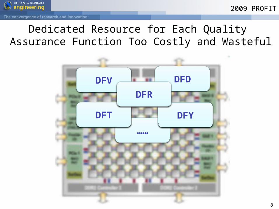
2009 PROFIT
……
Dedicated Resource for Each Quality Assurance Function Too Costly and Wasteful
DFD
DFT DFY
DFV
DFR

9
2009 PROFIT
Reusing On-Chip Functional Resources for Quality Assurance Functions
• Increasing the use of software-solution/system resources for detecting hardware failures
• Using on-chip communication and control infrastructure for test delivery and access
• Using cores to test each other
• …..
9

10
2009 PROFIT
Sharing DfX Circuitry for Multiple Quality Assurance Functions
• Generalize DfD ckt for runtime validation
• Extend validation monitors for on-line testing
• Reuse off-line calibration circuitry for in-field online tuning
• Share off-line BIST and on-line checking circuitry
• Reuse sensors for early-life failure/wearout detection to sense silicon data for silicon validation and manufacturing testing
debugging
DFD
Production testing
DFT
Runtime validation
OLC
In-field testing
OLT

11
2009 PROFIT
Time-Multiplexed On-Line Checking (TMOC) for Cost-Sensitive Applications
[ATS’08]• Online checker implemented in embedded FPGA
• Checking one block at a time in round-robin fashion
• Not interrupting normal operation
• Case Study: An H.264 Decoder design–Checkers: duplication+comparison–Checker fabrics: eFPGA–Significant area and power o/h reductions
Sub-System
A
Online Checker
of A
Sub-System
C
Sub-System
B
System on a Chip
Reconfi gurable Checker Space
TA TB TC TA...
TMOC Checker Operation Time Line
...
Nowt=TA
whent=TB
whent=TC

12
2009 PROFIT
Video and Document: http://cadlab.ece.ucsb.edu/~mgao/tmoc
Demo: TMOC on a Chip

13
2009 PROFIT
Sharing TMOC With Time-Multiplexed Assertion Checking (TMAC)
• TMOC infrastructure can be used for HW assertion checking as well
– checking sub-blocks in round-robin fashion without interrupting normal operation
eFPGA
scan channel
assertionviolation
Debugging information
Checker interface network
SoC Design
• Using coverage metrics to guide selection of assertions for hw implementation
• Adjustable area/power overheads and coverage/detection latency tradeoffs

14
2009 PROFIT
Digital-Assisted Analog Design Style Receiving Broad Acceptance
• Digital Calibration: Digitally-calibrated ADCs & RF transceivers– Goal: Linearity enhancement, mismatch compensation
• Digital Adaptation: Adaptive equalizer in high-speed serial links– Goal: Adapt to different operational environments
• Digitally-Intensive Design: All-digital PLL
• Testing is conducted after calibration/adaptation
Analog Circuits
Measurement
Tuning
Analog/RFInputs
Digital Processing Unit
Analog/DigitalOutputs

15
2009 PROFIT
15
Analog Circuits
MeasurementTuning
Analog/RFInputs
CalibrationCircuit
Analog/DigitalOutputs
ADCAdaptationEngine
DAC
Digital TapCoefficients
Scan In/out FF FF
Utilizing Digital Processing Unit for Post-Silicon Validation & Test
ExamplesBIST for all-digital PLL (Staszewski et. al., TCAS-II 07)
VCO frequency characterization (Demmerle, ITC06)
Testable adaptive equalizer (Lin & Cheng, ITC06, Abbas et al, DATE10)
Testable RF image-reject receiver (Chang & Cheng, ATS08)
Pipelined ADC calibration/testing (Chang et al., ISQED09, VTS09)
Analog pathobservabilityAnalog path
controllability
15

16
2009 PROFIT
Example: 3D Die-Stacking CMOS Image SensorArchitecture• Every ADC processes signals
from a X*Y CIS block• An ISP processes signals from
several ADCs
3D CIS Architecture
ISP Array
ADC Array
CIS Array
Pixel Array
ADC Array
ISP Array
Stacking• CIS to ADC array stacking
– Face-to-Face• ADC to ISP array stacking
– Through Silicon Via (TSV)

17
2009 PROFIT
Results of an ADC/TSV failure in 3D CISInterpolated Image
TSV to ISP Layer
P2S
Column Decoder
Ro
w D
ec
od
er
ADC1 ADC2
P2S
Image Signal Processor + Memory Unit
Pixel Array
ADC Array
ISP Array
TSV to ISP Layer
Microbump Microbump
ADC2
P2S
TSV to ISP Layer
Microbump

18
2009 PROFIT
Proposed Pixel-Interleaving Design Improves Error Tolerance
Capability*
• Alter CIS output connections: outputs of nearby sensors are connected to different ADCs– Utilize de-noise schemes to achieve error
tolerance• Suggest to interleave only the columns, not rows
– To conform to current column & row decoding scheme
Cross-sectional View
CIS Array
ADC ArrayADC 1 ADC 2 ADC 3
TSV1 TSV2 TSV3
* Joint work of UCSB and ITRI* Ref: 3D Workshop at DATE 2010
19
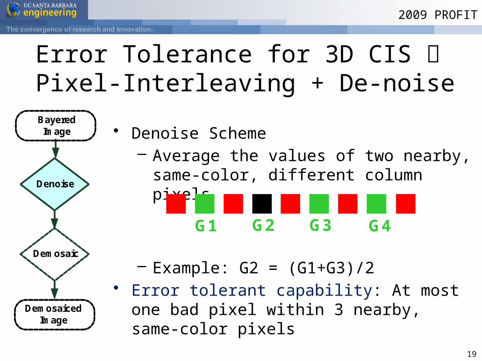
2009 PROFIT
Error Tolerance for 3D CIS Pixel-Interleaving + De-noise
• Denoise Scheme– Average the values of two nearby,
same-color, different column pixels
– Example: G2 = (G1+G3)/2• Error tolerant capability: At most one bad
pixel within 3 nearby, same-color pixels
G1 G2 G3 G4
Demosaic
Demosaiced Image
Denoise
BayeredImage

20
2009 PROFIT
Cost of Pixel-Interleaving
Wiring network: at column decoder output and at column output
Data rearrangement at the ISP

21
2009 PROFIT
Pixel-Interleaving 3D CISImage Quality under different N
Interpolated Image
PSNR = 23.33dB
M =64, N = 1Interpolated Image Interpolated Image
PSNR = 49.39dBPSNR = 23.89dB
M =64, N = 2 M =64, N = 3

22
2009 PROFIT
Interleaving helps maintain image qualityand improvement saturates after certain N
One defective ADC, results of 24 Benchmark Images, M=32
Ref: Chang et al, 3D Workshop at DATE 2010
23
2009 PROFIT
Other New Challenges (and Research Opportunities)
• Verification, validation, and test for error-resilient chips/systems
• Coverage metrics for post-Si and system validation [Lisherness and Cheng, HLDVT 2009]
– Measure of observability• Ignored by many functional metrics
– High-level compatibility• Efficient large-scale simulation• Support TLM and ad-hoc functional models• Support HLS design

24
2009 PROFIT
What is Flexible Electronics• Thin-film, light-weight, and low-cost• Bendable, durable, and large-area• Flexible substrates
– Plastics and metal foils– Non-photolithography manufacturing
• Ink-jet printing• Reel-to-reel imprinting
[1]
[2]
[1] Roll-to-roll process, PolyIC; [2] Ink-jet printed electronics, Phillips
Si MOFET
TFT
Performance
Cost

25
2009 PROFIT
• Applications– Non-destructive structure detectors– Flexible solar cells– Flexible displays – Biometrics — Lab-on-Chip– Wearable electronics and displays
Applications of Flexible Electronics
© PolyIC
© Univ. Tokyo © Univ. Tokyo
© Univ. Tokyo
© Seiko Epson
© Univ. Tokyo
© PolyIC
year04 05 06 07

26
2009 PROFIT
26
Key Difference with CMOSSi MOSFET A-Si:H TFT Organic TFT Oxide TFT
Process Temperature 1000 °C 250 °C Room Temp. 150 °C
ProcessTechnology
Photo-lithography
Photo-lithography
Roll-to-Roll / Ink-Jet
RFSputtering
Min. Length <= 65 nm 10 μm 50 μm 10 μm
Substrate Si WaferGlass
/PlasticPlastic/
Metal FoilGlass
/Plastic
Device Type N- & P-type N-type P-type N-type
Mobility 1500 cm2/V-s 1 cm2/V-s 0.5 cm2/V-s > 10 cm2/V-s
Cost/Area High Medium Low Low
Lifetime Years Months Weeks Years

27
2009 PROFIT
Key Reliability Challenges
Electrical degradation (A-Si TFT)Prolonged bias-stress on TFTs changes their properties and
varies the threshold voltage (VTH)Solutions: low-duty ratio operation, memorizing VTH with
capacitors Chemical degradation (Organic TFT)
Ambient oxygen and water vapor will dope the semiconducting material, change its properties, and vary VTH and ION/IOFF ratio
Solutions: material, packaging, substrate
G
Dielectric
Semiconductor
S D SSubstrate L
O2
O2
O2O2
O2
O2
O2 O2
H2O
H2OH2O
H2OH2O
H2O
H2O H2O
H2OO2
O2
O2
O2
O2O2
O2
O2
O2
H2O
H2O H2OH2O
H2O
H2O
H2O
H2O
H2O H2O
H2O H2O
H2O
O2O2 O2O2O2 O2
O2

28
2009 PROFIT
Research Opportunities on D&T for Reliable Flexible Electronics
• Reliability simulation platform*– Reliability analysis, modeling, and simulation
• System solutions for reliability enhancement**– Robust design for unreliable devices***– Post-manufacturing self-test and self-tunable
design– Array-based test flow
• Design-for-printability for roll-to-roll process– Substrate-aware physical design methodology– Self-aligned layer-to-layer patterning
* Huang et al, DAC 2007** Huang and Cheng, Journal of Display Technologies, 2008*** Huang et al, DATE 2010 (joint of UCSB, U of Tokyo, and ITRI)

29
2009 PROFIT
29
Summary Scaling and growing complexity challenge test and
its interaction with validation and emerging issues of variability and reliability
Test should be part of a total quality assurance solution
Test solutions should become more application- and system-aware
Test should maximize sharing of DFX resources with other post-silicon tasks
Abundant research opportunities on design and test for reliable flexible electronics