0.7 NA DUV STEP & SCAN SYSTEM FOR 150nm IMAGING …0.7 NA DUV STEP & SCAN SYSTEM FOR 150nm IMAGING...
20
0.7 NA DUV STEP & SCAN SYSTEM FOR 150nm IMAGING WITH IMPROVED OVERLAY Jan van Schoot, Frank Bornebroek, Manfred Suddendorf, Melchior Mulder, Jeroen van der Spek, Jan Stoeten and Adolph Hunter ASML BV De Run 1110, 5503 LA, Veldhoven, The Netherlands Peter Rümmer Carl Zeiss D-73446 Oberkochen, Germany This paper was first presented at the SPIE Symposium on Optical Microlithography March 1999, Santa Clara, California, USA
Transcript of 0.7 NA DUV STEP & SCAN SYSTEM FOR 150nm IMAGING …0.7 NA DUV STEP & SCAN SYSTEM FOR 150nm IMAGING...

0.7 NA DUV STEP & SCAN SYSTEM FOR 150nm IMAGINGWITH IMPROVED OVERLAY
Jan van Schoot, Frank Bornebroek, Manfred Suddendorf, Melchior Mulder,Jeroen van der Spek, Jan Stoeten and Adolph Hunter
ASML BVDe Run 1110, 5503 LA, Veldhoven, The Netherlands
Peter Rümmer
Carl ZeissD-73446 Oberkochen, Germany
This paper was first presented at theSPIE Symposium on Optical Microlithography
March 1999, Santa Clara, California, USA

1
0.7 NA DUV STEP & SCAN SYSTEM FOR 150nm IMAGING WITH IMPROVED OVERLAY
Jan van Schoot, Frank Bornebroek, Manfred Suddendorf, Melchior Mulder,Jeroen van der Spek, Jan Stoeten and Adolph Hunter
ASML BV, De Run 1110, 5503 LA Veldhoven, The Netherlands
Peter RümmerCarl Zeiss, D-73446 Oberkochen, Germany
ABSTRACT
To extend KrF lithography below the 180nm SIA design rule node in manufacturing, an advanced DUV Step & Scansystem utilizing a lens with an NA up to 0.7 will be required to provide sufficient process latitude [1]. Towards theSIA’s 150nm design rule node, manufacturing challenges for 248nm lithography include contact hole printing,iso-dense bias control and adequate across the field CD uniformity. All will benefit from higher NA lenses.
In this paper, results obtained on a PAS 5500/700B DUV Step & Scan system are presented. The system design isbased on the PAS 5500/500[2, 3] with a new 0.7NA Starlith™ lens, AERIAL™ II illuminator and ATHENA advancedalignment system. Imaging of dense and isolated lines at 180nm, 150nm and below as well as 180nm and 160nmcontact holes is shown.
In addition to imaging performance, image plane deviation, system distortion fingerprints, single-machine overlayand multiple-machine matching results are shown. Using the ATHENA alignment system, alignment reproducibilityas well as overlay results on CMP wafers will be shown.
It is concluded that this exposure tool is capable of delivering imaging and overlay performance required for massproduction at the 150nm design rule node, with potential for R&D applications beyond.
1. INTRODUCTION
The announcement of the 1997 National TechnologyRoad Map for Semiconductors brought into sharpfocus many of the challenges which IC manufacturersand equipment manufacturers together will have toovercome. Compared with the 1994 version of theroad-map, the timing for first production output ofseveral nodes had been accelerated. See Figure 1.
In particular the “First Product Shipment TechnologyGeneration” date for 180nm devices had beenadvanced from 2001 to 1999, 130nm Technology
Figure 1 The SIA Roadmap for Semiconductors.
Year: 95 96 97 98 99 00 01 02 03 04 05 06 07
NTRS'94
NTRS'97
1/2 pitch* 350 250 180 150 130 100Isol line* 200 140 120 100 70
* Dimensions for minimum half pitch and isolated line in nm
inserted
I-12
698.
ILL
Generation from 2004 to 2003, and a new node for a150nm Technology Generation first shipment in 2001was introduced for the first time. In October of 1998 aproposal for further acceleration was made when “FirstProduct Shipment” was revised to “Year of First VolumeShipment”, with the request for development capabilityto be available 2-3 years earlier [4]. The aggressiveacceleration of the road-map paves the way for a rapidtransition from 180nm to 150nm production. The timingof which can only be met by the extension of KrF DUVlithography beyond it’s previously recognizedapplication limit of 180nm.
The new timing essentially validated the alreadyon-going development of a new generation of high NADUV exposure tools. To meet the technological andtiming requirements of the road-map, IC manufacturersrequire a step and scan tool which is capable of 150nmproduction and available for R&D and pilot productionin the first half of 1999.
Optical system design and dynamic stage controlcritically determine the resulting imaging performanceof step and scan lithography systems. High NA lensescapture more of the higher orders diffracted by thereticle, thus allowing for a more precise reconstruction

2
of the pattern from the reticle. This results in a higherresolution, a larger exposure latitude, a smalleriso-dense bias, a smaller Mask Error Factor [12] etc.Regarding required lens NA, simulation studies usingSolid C, full resist model show that for 150nm L/S,maximum Exposure Latitude (EL) is optimal atNA>0.68, see Figure 2. In Figure 3 the Iso-Dense bias,calculated using the same model, is shown. It is alsoclear here that for 150nm production, DUV tools withhigher NA capability are required.
The PAS 5500/700B utilizes the PAS 5500 architectureand dynamic stage control systems proven in otherASML Step & Scan tools. Commonality in architecturebetween the PAS 5500/700B and other ASML Step &Scan tools facilitates an economical fab mix for critical,non-critical and back-end layer exposures. Waferstage scanning speeds of up to 250mm/s arecombined with on-the-fly levelling, while the ATHENAadvanced alignment system, together with the existingThrough-The-Lens (TTL) Phase Grating Alignment(PGA) system enables the PAS 5500/700B to deliverthe required overlay performance.
In this paper we describe the major systemenhancements of the PAS 5500/700B namely theProjection Lens, AERIAL™ II Illuminator and ATHENAmodule. Finally imaging and overlay results thatdemonstrate the 150nm production capability of thetool are presented.
2. GENERAL SYSTEM DESCRIPTION
The major new components of the PAS 5500/700BStep & Scan system are a 4X, NA = 0.70 projectionlens, AERIAL™ II high transmission illuminator and
ATHENA advanced alignment system. The newStarlith™ 700 lens is a variable 0.70 - 0.50NA lens.Printing at a lower K1 factor, even at 0.7NA, requires aprojection lens with low aberrations. Due to enhancedmanufacturing methods, the lens specifications areimproved compared to earlier DUV lens designs. Thenew AERIAL™ II illuminator is based on the illuminatordeveloped for the PAS 5500/900 193nm Step & Scansystem [5].
Imaging performance of a scanning system is stronglydetermined by the synchronization between reticle andwafer stage during exposure [6]. Stage synchronizationis characterized by Moving Standard Deviation (MSD)and Moving Average (MA) of the relative position ofboth stages over the time window in which each imagepoint travels across the illumination slit width. MArepresents a real stage error and contributes to theimage distortion and overlay budget. MSD describesthe loss of contrast (fading) of the aerial image thatresults from poor scan synchronization. Figure 4showsthe results of simulations for the relation between CDuniformity and MSD for various resolutions.
Simulations were performed using Solid C. The aerialimage is convoluted with the Gaussian distributedpositioning error. Also z-fading is taken into account ata fixed value of MSDz = 40nm. For the development aWeiss model is used with a resist contrast of 9.Exposure variations of ±4% around Best Energy areintroduced in order to incorporate exposure and reticleerrors, and thickness variations of the photoresistlayer. The CD-range at MSD=0 is taken as a reference.A lens/illuminator setting of NA = 0.70, σ = 0.85/0.55 isassumed. Decreasing the NA will enlarge the influenceof MSD, especially on the dense lines.
Figure 2 Maximum Exposure Latitude for 150nmdense lines.
7 8 9 10 11 12 13
NA
oute
r
0.65
0.70
0.75
0.80
0.85
0.60 0.62 0.64 0.66 0.68 0.70
I-12
699.
ILL
Figure 3 Iso-Dense Bias for 150nm dense lines.
10 20 30 40 50 60 70 80
NA
0.65
0.70
0.75
0.80
0.85
0.60 0.62 0.64 0.66 0.68 0.70
oute
r
I-12
700.
ILL
3
These simulations show that low MSD is a majorprerequisite for good imaging at low resolutions. Forthe PAS 5500/700B further improvements areachieved to bring the MA back to 5nm and MSD to15nm so together with the higher NA lens, 150nm iswithin the range of the system. Figure 5 shows peakMA and MSD values measured on a PAS 5500/700Bsystem. Data is collected over 7 wafers at themaximum Wafer Stage scan speed of 250 mm/s. Table1 shows the maximum, mean and mean + 3σ values.
The requirement for 150nm resolution as defined bythe SIA roadmap is 50nm for matched machineoverlay. From this a single machine overlay of 35nmcan be derived. The PAS 5500/700B is equipped withASML’s (TTL) Phase Grating Alignment system andthe ATHENA alignment system, ASML’s advancedPhase Grating Alignment system [7].
ATHENA has been developed as an addition to thecurrent TTL alignment system to meet the current andfuture overlay requirements especially on processedCMP layers. ATHENA is used to align the wafer withrespect to the wafer stage. The TTL system aligns thereticle to the wafer stage. ATHENA is able to collectindependently the signals of 7 diffraction orders at 2different wavelengths (633nm & 532nm).
Figure 4 MSD contribution to CD-uniformity. Forfeatures below 180nm, MSD valuesgreater than 20nm have a severe impacton the CD-uniformity.
0 10 20 30 40 50 60
MSD [nm]
25
20
15
10
5
0Con
trib
utio
n to
CD
U [n
m]
130nm
150nm
180nmI-
1270
1.IL
L
Dense linesIsolated lines
MA-X MA-Y MSD-X MSD-Y
max: 2.8 3.8 13.1 12.5
mean: 1.6 2.5 7.7 6.9
m + 3σ: 2.5 3.4 11.9 10.7
Table 1 Maximum, Mean and Mean + 3σ for MA andMSD over 7 wafers per die at maximumspeed.
Figure 5 Peak MA and MSD values in X and Y over 7 wafers at maximum speed.
1.9 2.72.0
2.0
1.7
1.7
1.9
1.61.8
1.8
1.71.7
2.1
2.0
1.6
1.7
2.1
1.5
1.6
1.6
1.9
1.6
2.2 2.3
2.8
1.6
2.6
1.6
1.9
2.2
1.4
1.8 1.8
1.9
1.6
1.7
1.9
2.0
1.6
1.9
2.7
2.6
1.6
2.0 1.71.7
PAS 5500 /700: WR peak MA-X & MA-Y
I-12
702.
ILL
2.8 3.53.8
3.1
2.7
2.8
2.8
2.83.0
3.0
2.92.9
3.1
2.2
3.0
2.8
3.2
3.0
2.7
2.7
3.2
2.4
2.8 2.8
3.0
2.5
2.9
2.3
3.6
2.6
2.8
3.0 2.9
3.1
2.5
2.6
2.8
3.1
3.3
2.5
2.5
2.7
2.4
2.8 2.62.5
12.5 12.411.0
7.0
7.0
7.1
12.4
6.87.3
7.7
6.57.5
7.1
8.3
7.9
7.9
10.2
10.3
7.3
8.2
7.5
8.5
7.7 9.8
6.6
7.5
8.5
6.6
7.8
7.2
7.3
8.6 8.3
7.4
7.3
9.5
7.5
8.9
8.6
9.2
10.1
12.4
6.6
6.8 7.69.1
PAS 5500 /700: WR peak MSD-X & MSD-Y
I-12
709.
ILL
10.0 12.111.9
8.2
9.4
8.4
8.5
8.38.1
7.9
8.99.4
8.6
12.4
7.7
7.7
8.6
8.5
7.7
10.0
8.3
8.0
9.9 8.6
8.3
7.7
8.2
8.3
9.5
8.5
7.5
9.1 8.6
9.4
8.6
8.4
10.0
10.0
9.4
12.1
13.1
12.2
7.7
7.4 7.58.6
4
Using 2 lasers eliminates destructive interference thatmay occur in deep marks or on marks covered withmultiple process layers. Additionally, it enables adesign of an optical system that detects eachdiffraction order on a separate detector. Thecombination of high power lasers and separatedetection of orders also guarantees sufficient signalstrength at shallow marks. Per wafer mark up to 14aligned positions, each associated with an individualdiffraction order, can be determined. Alignment recipescan select the optimum combination of these positionsyielding accurate alignment. This flexibility makesATHENA adaptable to any wafer process. A standardset of recipes is supplied. An established applicationprocedure enables the user to further optimize astandard recipe.
For both the ATHENA and TTL systems, improvedelectronics and software have been developed. Dataacquisition and data processing are now performed inparallel enhancing throughput by up to 8%, enabling athroughput of 104 wafers/hour (46 exposures,16x33mm field, 30mJ/cm2).
The ATHENA sensor is mounted just above the waferplane. A single frame made out of very low expansionmaterial holds the optical elements as depicted inFigure 6.
Baseline stability is maintained by referencing to afixed target on the wafer stage, that is also measuredby the TTL alignment system.
The lens system images all diffraction orders onindividual references on a single plate to guaranteemutual stability. The beam splitter separates bothwavelengths and the subsequent special opticalcomponents direct every pair of diffraction orderstowards its own reference grating. Aberrations of thealignment optics can easily be corrected for byapplying software off-sets to the individual signals. Thedetected light is transmitted towards the detectorswhich have been integrated with the electronics thatprocess the electrical signals.
A CCD camera provides a monitor image for visualinspection.
Figure 6 ATHENA hardware. On the right side, both lasers have been schematically depicted. Fibers guide thelaser light towards the ATHENA optical module (left hand side). Diffraction orders as reflected by thewafer target are imaged upon separate references. Subsequently, the light is transferred to a series ofdetectors.
Wafer mark
Detectors
Detectors
Modulator
Modulator
Wavelength 1
Wavelength 2
CCD
I-12
703.
ILL
5
The two lasers are contained in a separate box withcooling fans and optical isolators to guarantee theirstability. The laser light is modulated and polarized.Lasers, CCD camera and electronics are placed atremote locations where they are not able to influencethe temperature stable environment of the ATHENAoptical module.
The basic ATHENA performance (as measured on aPAS 5500/500) can be expressed in alignmentreproducibility per order, long-term stability anddynamic range, see Figures 7 to 9. Single-machineoverlay and overlay performance on processed (CMP)wafers will be presented in section 5.
3. THE PROJECTION SYSTEM
3.1 Design goals optical column
3.1.1 Projection lens
The Starlith™ 700 projection lens surpasses theStarlith™ 500 lens design [2] by an increased NA of 0.7and improved imaging quality. In addition to a reductionof the distortion, focal plane deviation and telecentricityvalues the lens was re-engineered with respect towavefront variance. The design part of the wavefrontaberrations budget could be reduced by more than 50%compared to the Starlith™ 500 lens used in the PAS5500/500 KrF step and scan system.
The excellent wavefront correction has twoadvantages: firstly it results in a very uniform imagingbehavior for a wide range of NA and σ settings forpartial coherent imaging. Secondly the contrast isconstant within a few percent over the full field. Bothsmall FPD values and high contrast over the field arefundamental to 150nm imaging capability. During thedesign process special care has been taken in order toachieve small incidence angles on the individual lenssurfaces. This eases both lens assembly and lenselement coating technology resulting in an improvedlens performance.
3.1.2 Illumination system
The design goals for the PAS 5500/700B-illuminatorwere threefold:
• Maximize the light intensity on wafer level byusing an improved optical design with fewerelements and shorter path length in opticalmaterials as well as improved anti-reflectiveand high-reflective coatings.For forming the pupil shape and theillumination field, diffractive optical elementshave been developed which guarantee highefficiencies.
• A high illuminator lifetime is obtained by usingselected quartz and CaF2-material for somelens elements and for the light mixing rod.Additionally, the whole illumination system ispurged with nitrogen gas in order to preventchemical and physical contamination.
Figure 7 ATHENA alignment reproducibility for eachof the different diffraction orders.
Figure 8 ATHENA long term stability.
Figure 9 ATHENA dynamic range.
0
1
2
3
4
5
All 1st 3rd 5th 7thDiffraction Order (Red and Green)
Alig
nem
nt r
epro
duci
bilit
y [S
tDev
, nm
] I-12
704.
ILL
-20100 20 30 40 50 60
-10
0
10
20
Time [min]
Alig
ned
Pos
ition
[nm
]
I-12
705.
ILL
0
5
10
15
20
Relative Alignment Signal
Alig
nmen
t Rep
rodu
cebi
lity
[StD
ev, n
m]
1st order
3rd order
5th order
7th order
10.0001 0.001 0.01 0.1
I-12
706.
ILL
6
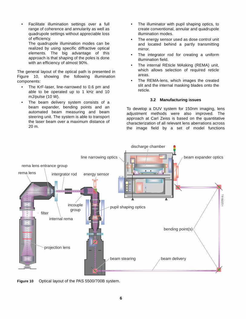
• Facilitate illumination settings over a fullrange of coherence and annularity as well asquadrupole settings without appreciable lossof efficiency.The quadrupole illumination modes can berealized by using specific diffractive opticalelements. The big advantage of thisapproach is that shaping of the poles is donewith an efficiency of almost 90%.
The general layout of the optical path is presented inFigure 10, showing the following illuminationcomponents:
• The KrF-laser, line-narrowed to 0.6 pm andable to be operated up to 1 kHz and 10mJ/pulse (10 W).
• The beam delivery system consists of abeam expander, bending points and anautomated beam measuring and beamsteering unit. The system is able to transportthe laser beam over a maximum distance of20 m.
• The illuminator with pupil shaping optics, tocreate conventional, annular and quadrupoleillumination modes.
• The energy sensor used as dose control unitand located behind a partly transmittingmirror.
• The integrator rod for creating a uniformillumination field.
• The internal REticle MAsking (REMA) unit,which allows selection of required reticleareas.
• The REMA-lens, which images the createdslit and the internal masking blades onto thereticle.
3.2 Manufacturing issues
To develop a DUV system for 150nm imaging, lensadjustment methods were also improved. Theapproach at Carl Zeiss is based on the quantitativecharacterization of all relevant lens aberrations acrossthe image field by a set of model functions
Figure 10 Optical layout of the PAS 5500/700B system.
rema lens
rema lens entrance group
line narrowing optics beam expander optics
intergrator rod
beam stearing beam delivery
pupil shaping optics
discharge chamber
bending point(s)
projection lens
filterinternal rema
incouplegroup
energy sensor
I-12
255.
ILL

7
implemented on the system qualification equipment asan integral part of the adjustment process. This allowsfor a systematic separation between the various ordersof rotational symmetric and non-symmetricaberrations. These aberrations can then be correctedfor by appropriate adjustment actions optimizing theconvergence of the adjustment quality. The rotationalsymmetric aberrations are adjusted close to the designvalues by varying the spacing between individual lenselements.
Further significant improvement was achieved byminimizing the non-rotational symmetric contributionswith respect to the scanner slit geometry usingdedicated algorithms to predict the best orientation ofthe optical elements. This advanced adjustmentapproach not only helps to ensure the production ofhigh-quality lenses at high output rates, but alsoassists in decreasing Ramp-Up time for new systemslike the Starlith™ 700 lens.
Implementation of computer-aided processesthroughout the whole production process has beenessential in achieving the volume production of 150nmDUV systems.
3.3 First system results
The Starlith™ 700 lens system shows improved opticalproperties compared to the NA = 0.63 Starlith™ 500and 550 lenses. Figure 11 shows the results of lensqualification measurements done at Carl Zeiss(scaling: Starlith™ 500 lens = 100%, Starlith™ 700data averaged over 6 lenses).
Maximum Zernike coefficients (lower coma, sphericalaberrations and threewave aberrations) measured byTTL interferometry over the used field are shown, aswell as the maximum of the wavefront RMS. Alsoshown are the maximum aberrations of the aerialimage for focal plane deviation, astigmatism anddistortion integrated in scanning direction.
The progressive reduction of the wavefront aberrationshas been achieved by extensive use of TTLinterferometry during the adjustment process. A largenumber of individual Zernike coefficients arecontrolled. This leads to a 0.7 NA lens withimprovements of more than 30% compared to a typicalStarlith™ 500 lens at NA = 0.63.
Similarly, the lens contribution to IPD, Astigmatism andDistortion has been reduced by up to 40% comparedto the Starlith™ 500 lens.
4. IMAGING RESULTS
4.1 Distortion and Focal Plane
The optical performance of the system has beenmeasured in terms of image distortion, focal plane andastigmatism. Both static and dynamic (scanning)results are shown in this section, representingprojection lens and system performance respectively.Test wafers were exposed and measured using theTTL alignment system of the PAS 5500/700B.
In static mode, measurements were taken at 13 x 3locations in the illumination slit. As the intensitydistribution in the illumination slit is trapezoidal in thescanning direction, static measurements are restrictedto an area in the centre of the slit, where the intensityis constant. At small sigma settings, this area ofconstant intensity is increased and thus allows thelargest number of sample points.
The full imaging field (26mm x 33mm) is used fordynamic measurements where 13 x 19 locations aresampled.
The usual corrections for residual adjustableparameters (static and dynamic) have been applied [2].
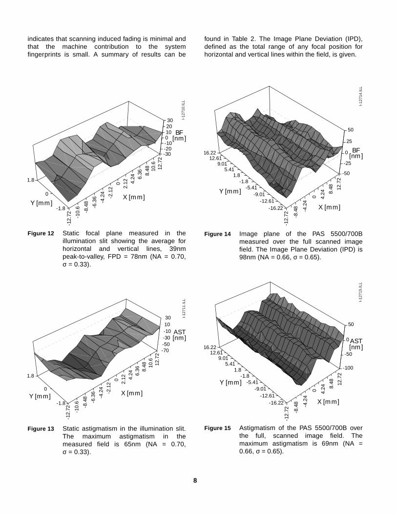
4.1.1 Image plane
The FOCAL technique [9] was used to determine focalplane and astigmatism. Static and dynamic results areshown in Figures 12 to 15. A visual comparison of thelens and system fingerprints clearly reveals thesimilarity between static and scanning results. This
Figure 11 Three generations of DUV projectionlenses. (Scale: Starlith™ 500 lens =100%).
0 %
20 %
40 %
60 %
80 %
100 %
Zernikecoefficients
WavefrontRMS
IntegratedFPD
Integrated IntegratedAstigmatism Distortion
Starlith™ 500 Starlith™ 550 Starlith™ 700
I-12
707.
ILL
8
indicates that scanning induced fading is minimal andthat the machine contribution to the systemfingerprints is small. A summary of results can be
found in Table 2. The Image Plane Deviation (IPD),defined as the total range of any focal position forhorizontal and vertical lines within the field, is given.
Figure 12 Static focal plane measured in theillumination slit showing the average forhorizontal and vertical lines, 39nmpeak-to-valley, FPD = 78nm (NA = 0.70,σ = 0.33).
Figure 13 Static astigmatism in the illumination slit.The maximum astigmatism in themeasured field is 65nm (NA = 0.70,σ = 0.33).
-12.
72 -10.
6
-8.4
8
-6.3
6
-4.2
4
-2.1
2
02.
12 4.24 6.
36 8.48 10
.612
.72
-1.8
0
1.8
-30-20-100102030
BF[nm]
X [mm]Y [mm]
I-12
710.
ILL
-12.
72 -10.
6
-8.4
8
-6.3
6
-4.2
4
-2.1
2
0 2.12 4.
24 6.36 8.
48 10.6
12.7
2
-1.8
0
1.8
-70-50-30-101030
AST[nm]
X [mm]Y [mm]
I-12
711.
ILL
Figure 14 Image plane of the PAS 5500/700Bmeasured over the full scanned imagefield. The Image Plane Deviation (IPD) is98nm (NA = 0.66, σ = 0.65).
Figure 15 Astigmatism of the PAS 5500/700B overthe full, scanned image field. Themaximum astigmatism is 69nm (NA =0.66, σ = 0.65).
-12.
72 -8.4
8 -4.2
4
0 4.24 8.
48 12.7
2
-16.22-12.61
-9.01-5.41
-1.81.8
5.419.01
12.6116.22
-50
-25
0
25
50
BF[nm]
X [mm]
Y [mm]
I-12
714.
ILL
-12.
72 -8.4
8 -4.2
4
0 4.24 8.
48 12.7
2
-16.22-12.61
-9.01-5.41
-1.81.8
5.419.01
12.6116.22
-100
-50
0
50
AST[nm]
X [mm]
Y [mm]
I-12
715.
ILL
9
4.1.2 Image distortion
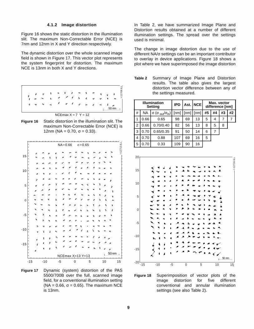
Figure 16 shows the static distortion in the illuminationslit. The maximum Non-Correctable Error (NCE) is7nm and 12nm in X and Y direction respectively.
The dynamic distortion over the whole scanned imagefield is shown in Figure 17. This vector plot representsthe system fingerprint for distortion. The maximumNCE is 13nm in both X and Y directions.
In Table 2, we have summarized Image Plane andDistortion results obtained at a number of differentillumination settings. The spread over the settingsused is minimal.
The change in image distortion due to the use ofdifferent NA/σ settings can be an important contributorto overlay in device applications. Figure 18 shows aplot where we have superimposed the image distortion
Figure 16 Static distortion in the illumination slit. Themaximum Non-Correctable Error (NCE) is12nm (NA = 0.70, σ = 0.33).
Figure 17 Dynamic (system) distortion of the PAS5500/700B over the full, scanned imagefield, for a conventional illumination setting(NA = 0.66, σ = 0.65). The maximum NCEis 13nm.
NCEmax X = 7 Y = 12
50 nm
I-12
708.
ILL
-15 -10 -5 0 5 10 15
NCEmax X=13 Y=13
-15
-10
-5
0
5
10
15
NA=0.66 =0.65
50nm
I-12
713.
ILL
Table 2 Summary of Image Plane and Distortionresults. The table also gives the largestdistortion vector difference between any ofthe settings measured.
IlluminationSetting IPD Ast. NCE Max. vector
difference [nm]
# NA σ (σ out/σin) [nm] [nm] [nm] #5 #4 #3 #2
1 0.66 0.65 98 69 13 5 4 7 7
2 0.66 0.70/0.40 82 56 13 8 5 8
3 0.70 0.65/0.35 91 50 14 6 7
4 0.70 0.88 107 69 16 5
5 0.70 0.33 109 90 16
Figure 18 Superimposition of vector plots of theimage distortion for five differentconventional and annular illuminationsettings (see also Table 2).
50 nm
I-12
716.
ILL20
15
10
5
0
-5
-10
-15
-15 -10 -5 0 5 10 15-20
10
vector plots for the illumination settings as listed inTable 2. The maximum non correctable distortiondifference between any of the settings measured isonly 8nm.
4.2 Resolution
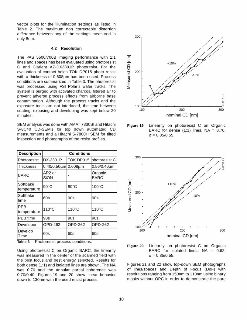
The PAS 5500/700B imaging performance with 1:1lines and spaces has been evaluated using photoresistC and Clariant AZ-DX3301P photoresist. For theevaluation of contact holes TOK DP015 photo resistwith a thickness of 0.608µm has been used. Processconditions are summarized in Table 3. The photoresistwas processed using FSI Polaris wafer tracks. Thesystem is purged with activated charcoal filtered air toprevent adverse process effects from airborne basecontamination. Although the process tracks and theexposure tools are not interfaced, the time betweencoating, exposing and developing was kept below 20minutes.
SEM analysis was done with AMAT 7830SI and HitachiS-8C40 CD-SEM’s for top down automated CDmeasurements and a Hitachi S-7800H SEM for tiltedinspection and photographs of the resist profiles.
Using photoresist C on Organic BARC, the linearitywas measured in the center of the scanned field withthe best focus and best energy selected. Results forboth dense (1:1) and isolated lines are shown. The NAwas 0.70 and the annular partial coherence was0.70/0.40. Figures 19 and 20 show linear behaviordown to 130nm with the used resist process.
Figures 21 and 22 show top-down SEM photographsof lines/spaces and Depth of Focus (DoF) withresolutions ranging from 150nm to 110nm using binarymasks without OPC in order to demonstrate the pure
Description Conditions
Photoresist DX-3301P TOK DP015 photoresist C
Thickness 0.40/0.50µm 0.608µm 0.56/0.40µm
BARCAR2 orSiON
-OrganicBARC
Softbaketemperature
90°C 80°C 100°C
Softbaketime
60s 90s 90s
PEBtemperature
110°C 110°C 110°C
PEB time 90s 90s 90s
Developer OPD-262 OPD-262 OPD-262
DevelopTime
60s 60s 60s
Table 3 Photoresist process conditions.
Figure 19 Linearity on photoresist C on OrganicBARC for dense (1:1) lines, NA = 0.70,σ = 0.85/0.55.
Figure 20 Linearity on photoresist C on OrganicBARC for isolated lines, NA = 0.62,σ = 0.85/0.55.
nominal CD [nm]
Mea
sure
d C
D [n
m]
+10%
-10%
100
200
300
100 200 300
I-12
718.
ILL
nominal CD [nm]
Mea
sure
d C
D [n
m]
+10%
-10%
100
200
300
100 200 300
I-12
717.
ILL

11
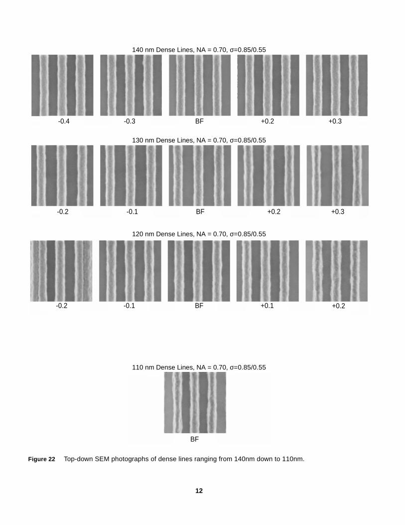
tool capability. Also 150nm isolated lines are shown.The illumination mode was annular for all cases. At theselected apertures and ring widths, the depth of focusis 0.8µm for 150nm dense lines, reducing to 0.5µm for130nm dense lines. For 150nm isolated lines, theobserved DoF is 0.5µm. At the bottom of Figure 22, itis shown that even a 110nm dense line pattern isresolved. For the used lens and illuminator setting, lessthan 10% of the light in the first orders is captured bythe lens, proving the nearly perfect image transfer bythe optical and mechanical systems.
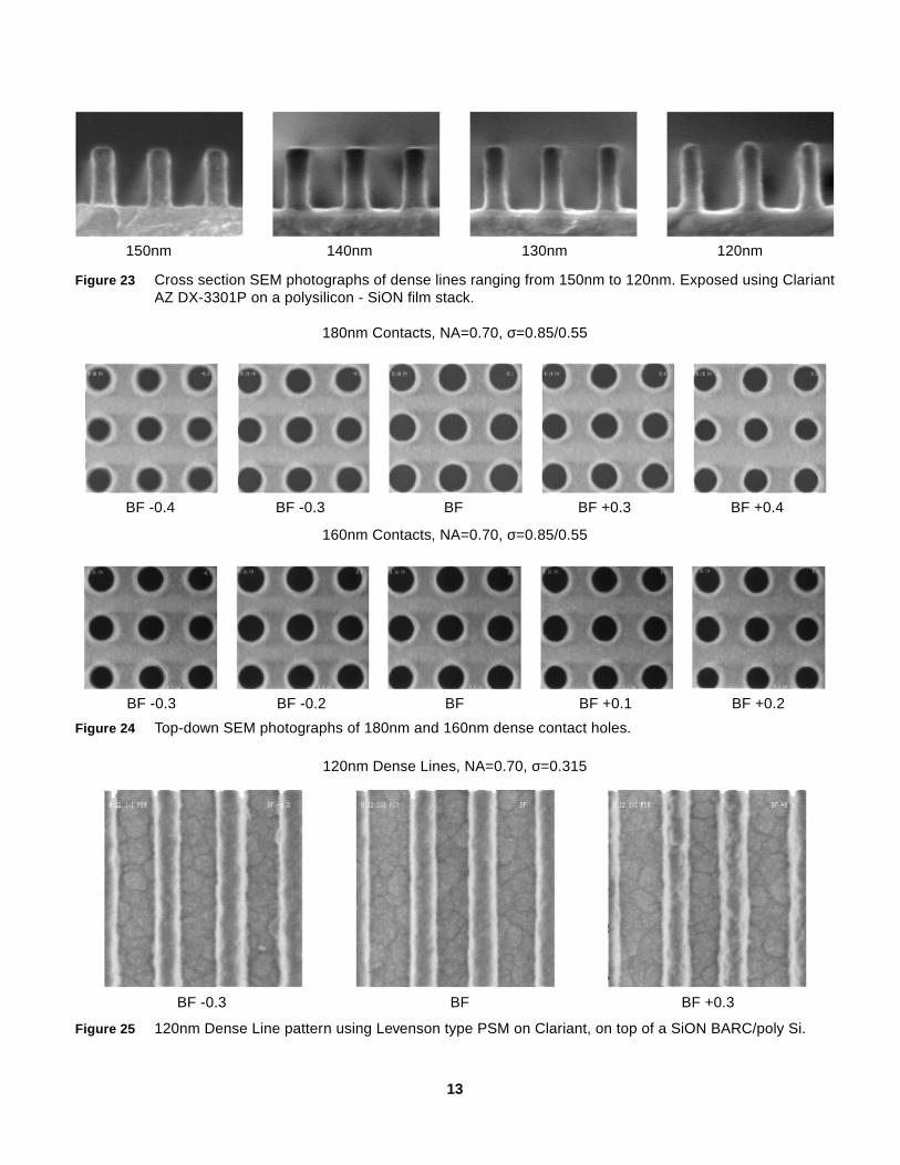
In Figure 23, SEM pictures of cross sections of denselines are shown, NA = 0.66, σ = 0.75/0.45 for the150nm exposure. All other pictures are obtained usingNA = 0.70, σ = 0.85/0.55.
Figure 24 shows top-down SEM pictures of 180nm and
160nm dense contact holes. The setting used wasNA = 0.70, σ = 0.85/0.55, the observed DoF is 0.8µmfor 180nm contacts, and 0.5µm for 160nm contacts.Note the roundness of the contact holes whichillustrates good dynamic stage control duringscanning.
All pictures shown in Figures 21 - 24 are made withbinary reticles without OPC, in order to show the puretool behavior.
CD-uniformity is an important measure forcharacterizing step and scan systems. TheCD-uniformity of 180nm and 150nm lines and spacesare measured, and the results are summarized inTable 4. In order to reduce SEM and processcontributions, six fields across the wafer are averagedat each field position.
150 nm Dense Lines, NA = 0.66, σ=0.75/0.45
150 nm Isolated Lines, NA = 0.62, σ=0.85/0.55
Figure 21 Top-down SEM photographs of 150nm dense and isolated lines.
BF +0.4+0.3-0.4 -0.3
BF +0.1 +0.2-0.3 -0.2
12
140 nm Dense Lines, NA = 0.70, σ=0.85/0.55
130 nm Dense Lines, NA = 0.70, σ=0.85/0.55
120 nm Dense Lines, NA = 0.70, σ=0.85/0.55
110 nm Dense Lines, NA = 0.70, σ=0.85/0.55
Figure 22 Top-down SEM photographs of dense lines ranging from 140nm down to 110nm.
BF-0.4 +0.3-0.3 +0.2
BF-0.1-0.2 +0.2 +0.3
+0.2-0.1-0.2 BF +0.1
BF
13
Figure 23 Cross section SEM photographs of dense lines ranging from 150nm to 120nm. Exposed using ClariantAZ DX-3301P on a polysilicon - SiON film stack.
140nm 130nm 120nm150nm
180nm Contacts, NA=0.70, σ=0.85/0.55
160nm Contacts, NA=0.70, σ=0.85/0.55
Figure 24 Top-down SEM photographs of 180nm and 160nm dense contact holes.
120nm Dense Lines, NA=0.70, σ=0.315
Figure 25 120nm Dense Line pattern using Levenson type PSM on Clariant, on top of a SiON BARC/poly Si.
BF -0.4 BF -0.3 BF BF +0.3 BF +0.4
BF -0.3 BF -0.2 BF BF +0.1 BF +0.2
BF -0.3 BF BF +0.3

14
Especially in the case of Dense Lines the reticlecontribution dominates the total measured CDvariation at best focus. The reticles used for theseexperiments are specially designed to minimize thereticle CD variation contribution using the “Picked CDtechnique” [10]. For the 150nm dense lines, the reticleCD distribution has a 3σ of 15nm. The Mask ErrorFactor (MEF)[11, 12] has been obtained experimentallyand equals 3.2. As a result, the expected 3σ at waferlevel is 12nm (15/4 *3.2). From this it can be concludedthat the reticle is responsible for approximately 80% ofthe entire CD uniformity.
Finally, in Figure 25 we show 120nm dense lines witha focus range of 0.6µm. These were obtained using anattenuated PSM. The asymmetry of the spaces is awell known effect using PSM and is due to reticleeffects [13].
5. OVERLAY PERFORMANCE
5.1 Introduction
In this section, the single machine overlayperformance of the PAS 5500/700B and the matchedmachine overlay performance of the PAS 5500/700B tothe PAS 5500/500 and to the PAS 5500/400 (I-linescanner) are presented. Additionally, results arepresented using the ATHENA system.
5.2 Single Machine Overlay
Figure 26 shows the single machine overlayperformance at full scan speed (250mm/s). On 8wafers, a layer of 20 full 26mm x 33mm fields wasexposed. After reloading the wafers in the machine andaligning them, an identical second layer was exposed.The maximum measured 99.7% single machineoverlay error between both layers was 14 and 18nm forX and Y, respectively. The ‘bell’-shape of the Gaussiancurve for the results in both the X and the Y direction iswell preserved.
In Figure 27, a detailed picture is shown of the overlayerrors of the first wafer. The errors are scaled withrespect to the single machine overlay specification of40nm (lower right corner).
Feature Setting
CD-uniformity [nm]
@BF ±0.1µm
±0.2µm
±0.3µm
180nm DL NA = 0.60,σ = 0.70/0.40 11 12 14
180nm iso NA = 0.56,σ = 0.60/0.30 9 23
150nm DL NA = 0.66,σ = 0.75/0.45 14 14 15
150nm DL* NA = 0.70,σ = 0.85/0.55 11 15
150nm iso NA = 0.62,σ = 0.85/0.55 11 19
*Quadrupole illumination has been used
Table 4 CD-uniformity 3σ values for 180nm and150nm dense and isolated features at bestfocus and over a focus range.
Figure 26 Single machine overlay at full scan speed:X = 14nm, Y = 18nm (99.7% of the data, 8wafers, 20 fields/wafer, 49 points/field).
Figure 27 Wafer plot of the first of 8 overlay wafers,showing 49 overlay vectors per field
0-40 -30 -20 -10 0 10 20 30 40
200
400
600
800
1000
1200
Overlay [nm]
Co
un
t
X
Y
I-1
27
27
.IL
L
-100
-50
0
50
100
-100 -50 0 50 100
Nom
inal
Pos
ition
Y [m
m]
Nominal Position X [mm]
40 nm
I-12
749.
ILL
15
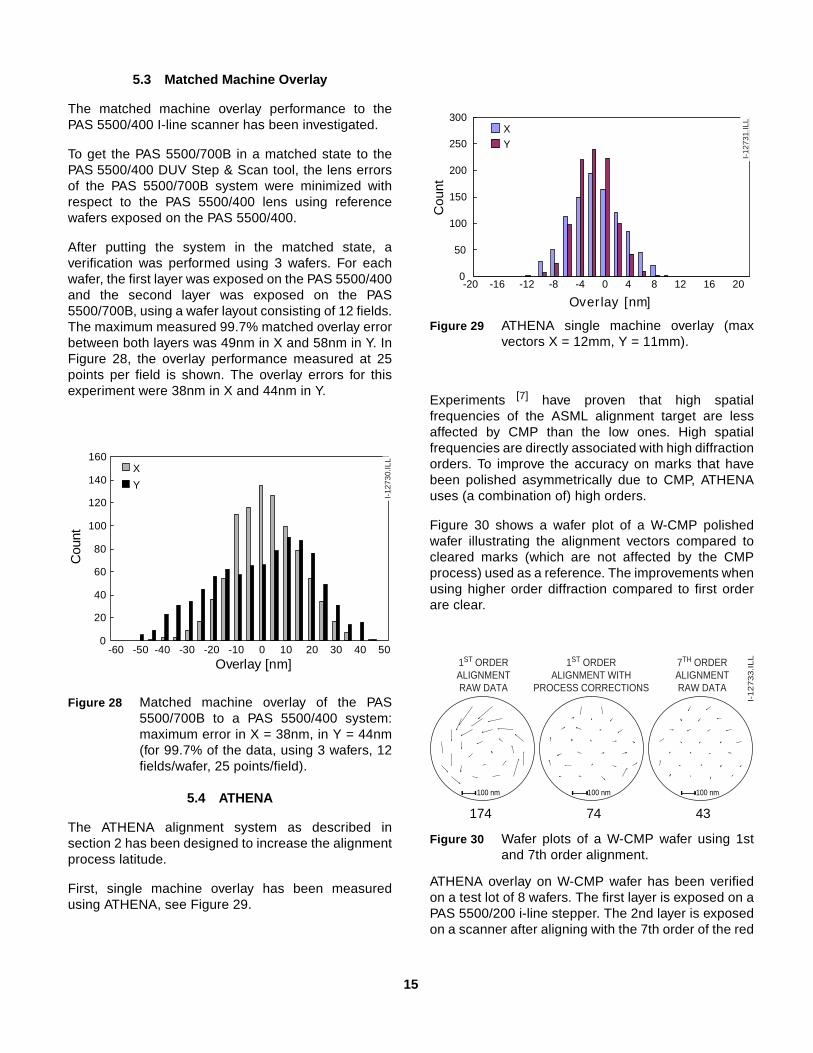
5.3 Matched Machine Overlay
The matched machine overlay performance to thePAS 5500/400 I-line scanner has been investigated.
To get the PAS 5500/700B in a matched state to thePAS 5500/400 DUV Step & Scan tool, the lens errorsof the PAS 5500/700B system were minimized withrespect to the PAS 5500/400 lens using referencewafers exposed on the PAS 5500/400.
After putting the system in the matched state, averification was performed using 3 wafers. For eachwafer, the first layer was exposed on the PAS 5500/400and the second layer was exposed on the PAS5500/700B, using a wafer layout consisting of 12 fields.The maximum measured 99.7% matched overlay errorbetween both layers was 49nm in X and 58nm in Y. InFigure 28, the overlay performance measured at 25points per field is shown. The overlay errors for thisexperiment were 38nm in X and 44nm in Y.
5.4 ATHENA
The ATHENA alignment system as described insection 2 has been designed to increase the alignmentprocess latitude.
First, single machine overlay has been measuredusing ATHENA, see Figure 29.
Experiments [7] have proven that high spatialfrequencies of the ASML alignment target are lessaffected by CMP than the low ones. High spatialfrequencies are directly associated with high diffractionorders. To improve the accuracy on marks that havebeen polished asymmetrically due to CMP, ATHENAuses (a combination of) high orders.
Figure 30 shows a wafer plot of a W-CMP polishedwafer illustrating the alignment vectors compared tocleared marks (which are not affected by the CMPprocess) used as a reference. The improvements whenusing higher order diffraction compared to first orderare clear.
ATHENA overlay on W-CMP wafer has been verifiedon a test lot of 8 wafers. The first layer is exposed on aPAS 5500/200 i-line stepper. The 2nd layer is exposedon a scanner after aligning with the 7th order of the red
Figure 28 Matched machine overlay of the PAS5500/700B to a PAS 5500/400 system:maximum error in X = 38nm, in Y = 44nm(for 99.7% of the data, using 3 wafers, 12fields/wafer, 25 points/field).
0
20
40
60
80
100
120
140
160
-60 -50 -40 -30 -20 -10 0 10 20 30 40 50Overlay [nm]
Cou
nt
X
Y
I-12
730.
ILL
Figure 29 ATHENA single machine overlay (maxvectors X = 12mm, Y = 11mm).
Figure 30 Wafer plots of a W-CMP wafer using 1stand 7th order alignment.
0
50
100
150
200
250
300
-20 -16 -12 -8 -4 0 4 8 12 16 20
Over lay [nm]
Cou
nt
XY
I-12
731.
ILL
I-12733.ILL
100 nm 100 nm 100 nm
7TH ORDERALIGNMENTRAW DATA
1ST ORDERALIGNMENTRAW DATA
1ST ORDERALIGNMENT WITH
PROCESS CORRECTIONS
174 74 43
16
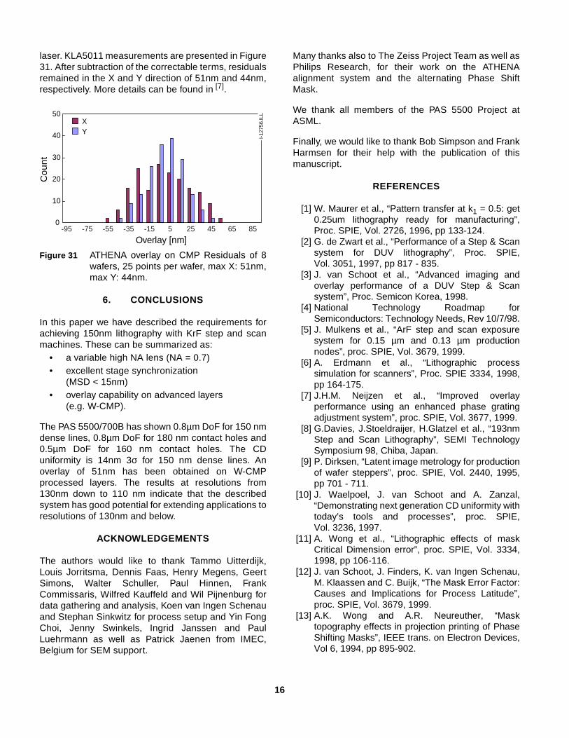
laser. KLA5011 measurements are presented in Figure31. After subtraction of the correctable terms, residualsremained in the X and Y direction of 51nm and 44nm,respectively. More details can be found in [7].
6. CONCLUSIONS
In this paper we have described the requirements forachieving 150nm lithography with KrF step and scanmachines. These can be summarized as:
• a variable high NA lens (NA = 0.7)• excellent stage synchronization
(MSD < 15nm)• overlay capability on advanced layers
(e.g. W-CMP).
The PAS 5500/700B has shown 0.8µm DoF for 150 nmdense lines, 0.8µm DoF for 180 nm contact holes and0.5µm DoF for 160 nm contact holes. The CDuniformity is 14nm 3σ for 150 nm dense lines. Anoverlay of 51nm has been obtained on W-CMPprocessed layers. The results at resolutions from130nm down to 110 nm indicate that the describedsystem has good potential for extending applications toresolutions of 130nm and below.
ACKNOWLEDGEMENTS
The authors would like to thank Tammo Uitterdijk,Louis Jorritsma, Dennis Faas, Henry Megens, GeertSimons, Walter Schuller, Paul Hinnen, FrankCommissaris, Wilfred Kauffeld and Wil Pijnenburg fordata gathering and analysis, Koen van Ingen Schenauand Stephan Sinkwitz for process setup and Yin FongChoi, Jenny Swinkels, Ingrid Janssen and PaulLuehrmann as well as Patrick Jaenen from IMEC,Belgium for SEM support.
Many thanks also to The Zeiss Project Team as well asPhilips Research, for their work on the ATHENAalignment system and the alternating Phase ShiftMask.
We thank all members of the PAS 5500 Project atASML.
Finally, we would like to thank Bob Simpson and FrankHarmsen for their help with the publication of thismanuscript.
REFERENCES
[1] W. Maurer et al., “Pattern transfer at k1 = 0.5: get0.25um lithography ready for manufacturing”,Proc. SPIE, Vol. 2726, 1996, pp 133-124.
[2] G. de Zwart et al., “Performance of a Step & Scansystem for DUV lithography”, Proc. SPIE,Vol. 3051, 1997, pp 817 - 835.
[3] J. van Schoot et al., “Advanced imaging andoverlay performance of a DUV Step & Scansystem”, Proc. Semicon Korea, 1998.
[4] National Technology Roadmap forSemiconductors: Technology Needs, Rev 10/7/98.
[5] J. Mulkens et al., “ArF step and scan exposuresystem for 0.15 µm and 0.13 µm productionnodes”, proc. SPIE, Vol. 3679, 1999.
[6] A. Erdmann et al., “Lithographic processsimulation for scanners”, Proc. SPIE 3334, 1998,pp 164-175.
[7] J.H.M. Neijzen et al., “Improved overlayperformance using an enhanced phase gratingadjustment system”, proc. SPIE, Vol. 3677, 1999.
[8] G.Davies, J.Stoeldraijer, H.Glatzel et al., “193nmStep and Scan Lithography”, SEMI TechnologySymposium 98, Chiba, Japan.
[9] P. Dirksen, “Latent image metrology for productionof wafer steppers”, proc. SPIE, Vol. 2440, 1995,pp 701 - 711.
[10] J. Waelpoel, J. van Schoot and A. Zanzal,“Demonstrating next generation CD uniformity withtoday’s tools and processes”, proc. SPIE,Vol. 3236, 1997.
[11] A. Wong et al., “Lithographic effects of maskCritical Dimension error”, proc. SPIE, Vol. 3334,1998, pp 106-116.
[12] J. van Schoot, J. Finders, K. van Ingen Schenau,M. Klaassen and C. Buijk, “The Mask Error Factor:Causes and Implications for Process Latitude”,proc. SPIE, Vol. 3679, 1999.
[13] A.K. Wong and A.R. Neureuther, “Masktopography effects in projection printing of PhaseShifting Masks”, IEEE trans. on Electron Devices,Vol 6, 1994, pp 895-902.
Figure 31 ATHENA overlay on CMP Residuals of 8wafers, 25 points per wafer, max X: 51nm,max Y: 44nm.
0
10
20
30
40
50
Overlay [nm]
Co
un
t
X Y
-95 -75 -55 -35 -15 5 25 45 65 85
I-127
56.IL
L


4022 502 94098


![:DUV]DZD GQLD U 9LPDQD 6ROXWLRQV 6S ] R R XO …](https://static.fdocuments.net/doc/165x107/61917b3011bd280eb20ee768/duvdzd-gqld-u-9lpdqd-6roxwlrqv-6s-r-r-xo-.jpg)