0 Virtex-5Q Family Overview - Xilinx · Virtex-5Q Family Overview DS174 (v2.0) March 22, 2010...
13
DS174 (v2.0) March 22, 2010 www.xilinx.com Product Specification 1 © Copyright 2009–2010 Xilinx, Inc. XILINX, the Xilinx logo, Virtex, Spartan, ISE, and other designated brands included herein are trademarks of Xilinx in the United States and other countries. PCI, PCI Express, PCIe, and PCI-X are trademarks of PCI-SIG. PowerPC is a trademark of IBM Corp. and is used under license. All other trademarks are the property of their respective owners. General Description The Defense-grade Virtex®-5Q family provides the newest, most capable features in the aerospace and defense industry from the reprogrammable FPGA market leader. The Virtex-5Q family delivers on Size, Weight, and Power - Cost (SWAP-C) reduction requirements while increasing performance and density for higher integration. Based on the proven commercial Virtex-5 FPGAs, the Virtex-5Q family offers greater operational temperature ranges off the shelf to fit the needs of the aerospace and defense customer base as well as ruggedized packaging for protection against tin-whiskering and harsh manufacturing processes. Mask-set control and long-term product availability are also standard. Using the second generation Advanced Silicon Modular Block (ASMBL™) column-based architecture, the Virtex-5Q family contains four distinct sub-families, the most offered by any FPGA vendor. Each sub-family contains a different ratio of features to address the needs of a wide variety of advanced designs. In addition to the most advanced, high-performance logic fabric, Virtex-5Q FPGAs contain many dedicated system-level blocks, including powerful 36 Kbit block RAM/FIFOs, second generation 25 x 18 DSP slices, SelectIO™ technology with built-in digitally-controlled impedance, ChipSync™ technology source-synchronous interface blocks, system monitor functionality, enhanced clock management tiles (CMTs) with integrated digital clock managers (DCM) and phase- locked-loop (PLL) clock generators, and advanced configuration options. Additional device-dependent features include power-optimized, high-speed serial transceiver blocks for enhanced serial connectivity, PCI Express® compliant integrated Endpoint blocks, tri-mode Ethernet Media Access Controllers (Ethernet MACs), and high-performance PowerPC® 440 microprocessor embedded blocks. These features allow advanced logic designers to build the highest levels of performance and functionality into their FPGA-based systems. The Virtex-5Q LX, LXT, SXT, and FXT FPGAs also include advanced high-speed serial connectivity and link/transaction layer capability. Virtex-5Q FPGAs offer the best solution for addressing the needs of aerospace and defense logic, DSP, and embedded systems designers for a host of applications including imaging, secure applications, electronic warfare, packet processing, and more. Summary of Virtex-5Q FPGA Features • Four sub-families: LX, LXT, SXT, and FXT • Virtex-5Q LX: High-performance general logic applications • Virtex-5Q LXT: High-performance logic with advanced serial connectivity • Virtex-5Q SXT: High-performance signal processing applications with advanced serial connectivity • Virtex-5Q FXT: High-performance embedded systems with advanced serial connectivity • Cross-family compatibility • LXT, SXT, and FXT devices are footprint compatible in the same package using adjustable voltage regulators • All devices are pin-to-pin compatible with commercial Virtex-5 devices with the same package within sub-families for prototyping. • Most advanced, high-performance, optimal-utilization, FPGA logic • Real 6-input look-up table (LUT) technology • Dual 5-LUT option • Improved reduced-hop routing • 64-bit distributed RAM option • SRL32/Dual SRL16 option • Powerful CMT clocking • DCM blocks for zero delay buffering, frequency synthesis, and clock phase shifting • PLL blocks for input jitter filtering, zero delay buffering, frequency synthesis, and phase-matched clock division • 36 Kbit block RAM/FIFOs • True dual-port RAM blocks • Enhanced optional programmable FIFO logic • Programmable - True dual-port widths up to x36 - Simple dual-port widths up to x72 • Built-in optional error-correction circuitry • Optionally program each block as two independent 18 Kbit blocks • High-performance parallel SelectIO technology • 1.2 to 3.3V I/O Operation • Source-synchronous interfacing using ChipSync technology • Digitally-controlled impedance (DCI) active termination • Flexible fine-grained I/O banking • High-speed memory interface support • Advanced DSP48E slices • 25 x 18, two’s complement, multiplication • Optional adder, subtracter, and accumulator • Optional pipelining • Optional bitwise logical functionality • Dedicated cascade connections • Flexible configuration options • SPI and Parallel Flash interface • Multi-bitstream support with dedicated fallback reconfiguration logic • Auto bus width detection capability • System Monitoring capability on all devices • On-chip/Off-chip thermal monitoring • On-chip/Off-chip power supply monitoring • JTAG access to all monitored quantities • Integrated Endpoint blocks for PCI Express designs • LXT, SXT, and FXT FPGAs • Compliant with the PCI Express Base Specification 1.1 • x1, x4, or x8 lane support per block • Works in conjunction with RocketIO™ transceivers • Tri-mode 10/100/1000 Mb/s Ethernet MACs • LXT, SXT, and FXT FPGAs • RocketIO transceivers can be used as PHY or connect to external PHY using many soft Media Independent Interface (MII) options • RocketIO GTP transceivers 100 Mb/s to 3.75 Gb/s • LXT and SXT FPGAs • RocketIO GTX transceivers 150 Mb/s to 6.5 Gb/s • FXT FPGAs only • PowerPC 440 microprocessors • FXT FPGAs only • RISC architecture • 7-stage pipeline • 32 Kbyte instruction and data caches included • Optimized processor interface structure (crossbar) • 65 nm copper CMOS process technology • 1.0V core voltage • Rugged EF packaging • Epoxy coated internal chip caps for superior solvent clean resistance (all except FF323 and FF1738 pin packages) • Fully tin/lead packaging including chip-cap finish 0 Virtex-5Q Family Overview DS174 (v2.0) March 22, 2010 0 0 Product Specification
Transcript of 0 Virtex-5Q Family Overview - Xilinx · Virtex-5Q Family Overview DS174 (v2.0) March 22, 2010...

DS174 (v2.0) March 22, 2010 www.xilinx.comProduct Specification 1
© Copyright 2009–2010 Xilinx, Inc. XILINX, the Xilinx logo, Virtex, Spartan, ISE, and other designated brands included herein are trademarks of Xilinx in the United States and other countries. PCI, PCI Express, PCIe, and PCI-X are trademarks of PCI-SIG. PowerPC is a trademark of IBM Corp. and is used under license. All other trademarks are the property of their respective owners.
General DescriptionThe Defense-grade Virtex®-5Q family provides the newest, most capable features in the aerospace and defense industry from the reprogrammable FPGA market leader. The Virtex-5Q family delivers on Size, Weight, and Power - Cost (SWAP-C) reduction requirements while increasing performance and density for higher integration. Based on the proven commercial Virtex-5 FPGAs, the Virtex-5Q family offers greater operational temperature ranges off the shelf to fit the needs of the aerospace and defense customer base as well as ruggedized packaging for protection against tin-whiskering and harsh manufacturing processes. Mask-set control and long-term product availability are also standard. Using the second generation Advanced Silicon Modular Block (ASMBL™) column-based architecture, the Virtex-5Q family contains four distinct sub-families, the most offered by any FPGA vendor. Each sub-family contains a different ratio of features to address the needs of a wide variety of advanced designs. In addition to the most advanced, high-performance logic fabric, Virtex-5Q FPGAs contain many dedicated system-level blocks, including powerful 36 Kbit block RAM/FIFOs, second generation 25 x 18 DSP slices, SelectIO™ technology with built-in digitally-controlled impedance, ChipSync™ technology source-synchronous interface blocks, system monitor functionality, enhanced clock management tiles (CMTs) with integrated digital clock managers (DCM) and phase-locked-loop (PLL) clock generators, and advanced configuration options. Additional device-dependent features include power-optimized, high-speed serial transceiver blocks for enhanced serial connectivity, PCI Express® compliant integrated Endpoint blocks, tri-mode Ethernet Media Access Controllers (Ethernet MACs), and high-performance PowerPC® 440 microprocessor embedded blocks. These features allow advanced logic designers to build the highest levels of performance and functionality into their FPGA-based systems. The Virtex-5Q LX, LXT, SXT, and FXT FPGAs also include advanced high-speed serial connectivity and link/transaction layer capability. Virtex-5Q FPGAs offer the best solution for addressing the needs of aerospace and defense logic, DSP, and embedded systems designers for a host of applications including imaging, secure applications, electronic warfare, packet processing, and more.
Summary of Virtex-5Q FPGA Features• Four sub-families: LX, LXT, SXT, and FXT
• Virtex-5Q LX: High-performance general logic applications• Virtex-5Q LXT: High-performance logic with advanced serial
connectivity• Virtex-5Q SXT: High-performance signal processing
applications with advanced serial connectivity• Virtex-5Q FXT: High-performance embedded systems with
advanced serial connectivity• Cross-family compatibility
• LXT, SXT, and FXT devices are footprint compatible in the same package using adjustable voltage regulators
• All devices are pin-to-pin compatible with commercial Virtex-5 devices with the same package within sub-families for prototyping.
• Most advanced, high-performance, optimal-utilization, FPGA logic• Real 6-input look-up table (LUT) technology• Dual 5-LUT option• Improved reduced-hop routing• 64-bit distributed RAM option• SRL32/Dual SRL16 option
• Powerful CMT clocking• DCM blocks for zero delay buffering, frequency synthesis,
and clock phase shifting• PLL blocks for input jitter filtering, zero delay buffering,
frequency synthesis, and phase-matched clock division• 36 Kbit block RAM/FIFOs
• True dual-port RAM blocks• Enhanced optional programmable FIFO logic• Programmable
- True dual-port widths up to x36- Simple dual-port widths up to x72
• Built-in optional error-correction circuitry• Optionally program each block as two independent 18 Kbit
blocks• High-performance parallel SelectIO technology
• 1.2 to 3.3V I/O Operation• Source-synchronous interfacing using ChipSync technology• Digitally-controlled impedance (DCI) active termination• Flexible fine-grained I/O banking• High-speed memory interface support
• Advanced DSP48E slices• 25 x 18, two’s complement, multiplication• Optional adder, subtracter, and accumulator• Optional pipelining• Optional bitwise logical functionality• Dedicated cascade connections
• Flexible configuration options• SPI and Parallel Flash interface• Multi-bitstream support with dedicated fallback
reconfiguration logic• Auto bus width detection capability
• System Monitoring capability on all devices• On-chip/Off-chip thermal monitoring• On-chip/Off-chip power supply monitoring• JTAG access to all monitored quantities
• Integrated Endpoint blocks for PCI Express designs• LXT, SXT, and FXT FPGAs• Compliant with the PCI Express Base Specification 1.1• x1, x4, or x8 lane support per block• Works in conjunction with RocketIO™ transceivers
• Tri-mode 10/100/1000 Mb/s Ethernet MACs• LXT, SXT, and FXT FPGAs• RocketIO transceivers can be used as PHY or connect to
external PHY using many soft Media Independent Interface (MII) options
• RocketIO GTP transceivers 100 Mb/s to 3.75 Gb/s• LXT and SXT FPGAs
• RocketIO GTX transceivers 150 Mb/s to 6.5 Gb/s• FXT FPGAs only
• PowerPC 440 microprocessors• FXT FPGAs only• RISC architecture• 7-stage pipeline• 32 Kbyte instruction and data caches included• Optimized processor interface structure (crossbar)
• 65 nm copper CMOS process technology• 1.0V core voltage• Rugged EF packaging
• Epoxy coated internal chip caps for superior solvent clean resistance (all except FF323 and FF1738 pin packages)
• Fully tin/lead packaging including chip-cap finish
0
Virtex-5Q Family Overview
DS174 (v2.0) March 22, 2010 0 0 Product Specification
Virtex-5Q Family Overview
DS174 (v2.0) March 22, 2010 www.xilinx.comProduct Specification 2
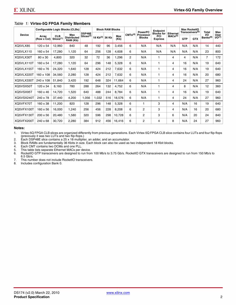
Table 1: Virtex-5Q FPGA Family Members
Device
Configurable Logic Blocks (CLBs)
DSP48E Slices(2)
Block RAM Blocks
CMTs(4)PowerPCProcessor
Blocks
EndpointBlocks for
PCI Express
EthernetMACs(5)
Max RocketIO Transceivers(6) Total
I/OBanks(8)
MaxUser I/O(7)Array
(Row x Col)CLB
Slices(1)
MaxDistributed RAM (Kb)
18 Kb(3) 36 Kb Max(Kb) GTP GTX
XQ5VLX85 120 x 54 12,960 840 48 192 96 3,456 6 N/A N/A N/A N/A N/A 14 440
XQ5VLX110 160 x 54 17,280 1,120 64 256 128 4,608 6 N/A N/A N/A N/A N/A 23 800
XQ5VLX30T 80 x 30 4,800 320 32 72 36 1,296 2 N/A 1 4 4 N/A 7 172
XQ5VLX110T 160 x 54 17,280 1,120 64 296 148 5,328 6 N/A 1 4 16 N/A 19 640
XQ5VLX155T 160 x 76 24,320 1,640 128 424 212 7,632 6 N/A 1 4 16 N/A 19 640
XQ5VLX220T 160 x 108 34,560 2,280 128 424 212 7,632 6 N/A 1 4 16 N/A 20 680
XQ5VLX330T 240 x 108 51,840 3,420 192 648 324 11,664 6 N/A 1 4 24 N/A 27 960
XQ5VSX50T 120 x 34 8,160 780 288 264 132 4,752 6 N/A 1 4 8 N/A 12 360
XQ5VSX95T 160 x 46 14,720 1,520 640 488 244 8,784 6 N/A 1 4 16 N/A 19 640
XQ5VSX240T 240 x 78 37,440 4,200 1,056 1,032 516 18,576 6 N/A 1 4 24 N/A 27 960
XQ5VFX70T 160 x 38 11,200 820 128 296 148 5,328 6 1 3 4 N/A 16 19 640
XQ5VFX100T 160 x 56 16,000 1,240 256 456 228 8,208 6 2 3 4 N/A 16 20 680
XQ5VFX130T 200 x 56 20,480 1,580 320 596 298 10,728 6 2 3 6 N/A 20 24 840
XQ5VFX200T 240 x 68 30,720 2,280 384 912 456 16,416 6 2 4 8 N/A 24 27 960
Notes: 1. Virtex-5Q FPGA CLB slices are organized differently from previous generations. Each Virtex-5Q FPGA CLB slice contains four LUTs and four flip-flops
(previously it was two LUTs and two flip-flops.)2. Each DSP48E slice contains a 25 x 18 multiplier, an adder, and an accumulator.3. Block RAMs are fundamentally 36 Kbits in size. Each block can also be used as two independent 18 Kbit blocks.4. Each CMT contains two DCMs and one PLL.5. This table lists separate Ethernet MACs per device.6. RocketIO GTP transceivers are designed to run from 100 Mb/s to 3.75 Gb/s. RocketIO GTX transceivers are designed to run from 150 Mb/s to
6.5 Gb/s.7. This number does not include RocketIO transceivers.8. Includes configuration Bank 0.

Virtex-5Q Family Overview
DS174 (v2.0) March 22, 2010 www.xilinx.comProduct Specification 3
Virtex-5Q FPGA Logic• On average, one to two speed grade improvement over
Virtex-4 devices• Cascadable 32-bit variable shift registers or 64-bit
distributed memory capability• Superior routing architecture with enhanced diagonal
routing supports block-to-block connectivity with minimal hops
• Up to 330,000 logic cells including:
• Up to 207,360 internal fabric flip-flops with clock enable (XQ5VLX330T)
• Up to 207,360 real 6-input LUTs with greater than 13 million total LUT bits
• Two outputs for dual 5-LUT mode give enhanced utilization
• Logic expanding multiplexers and I/O registers
500 MHz Clock Technology• Up to six CMTs
• Each CMT contains two DCMs and one PLL—up to eighteen total clock generators
• Flexible DCM-to-PLL or PLL-to-DCM cascade
• Precision clock deskew and phase shift
• Flexible frequency synthesis
• Multiple operating modes to ease performance trade-off decisions
• Improved maximum input/output frequency
• Fine-grained phase shifting resolution
• Input jitter filtering
• Low-power operation
• Wide phase shift range
• Differential clock tree structure for optimized low-jitter clocking and precise duty cycle
• 32 global clock networks• Regional, I/O, and local clocks in addition to global
clocks
SelectIO Technology• Up to 960 user I/Os• Wide selection of I/O standards from 1.2V to 3.3V• Extremely high performance
• Up to 800 Mb/s HSTL and SSTL (on all single-ended I/Os)
• Up to 1.25 Gb/s LVDS (on all differential I/O pairs)
• True differential termination on-chip• Same edge capture at input and output I/Os• Extensive memory interface support
500 MHz Integrated Block Memory• Up to 18.1 Mb of integrated block memory, assuming
Mb = 220 bits• 36 Kbit blocks with optional dual 18 Kbit mode• True dual-port RAM cells• Independent port width selection (x1 to x72)
• Up to x36 total per port for true dual port operation
• Up to x72 total per port for simple dual port operation (one Read port and one Write port)
• Memory bits plus parity/sideband memory support for x9, x18, x36, and x72 widths
• Configurations from 32K x 1 to 512 x 72 (8K x 4 to 512 x 72 for FIFO operation)
• Multirate FIFO support logic• Full and Empty flag with fully programmable Almost Full and
Almost Empty flags
• Synchronous FIFO support without Flag uncertainty• Optional pipeline stages for higher performance• Byte-write capability• Dedicated cascade routing to form 64K x 1 memory
without using FPGA routing• Integrated optional ECC for high-reliability memory
requirements• Special reduced-power design for 18 Kbit (and below)
operation
500 MHz DSP48E Slices• 25 x 18 two’s complement multiplication
• Optional pipeline stages for enhanced performance
• Optional 48-bit accumulator for multiply accumulate (MACC) operation with optional accumulator cascade to 96 bits
• Integrated adder for complex-multiply or multiply-add operation
• Optional bitwise logical operation modes
• Independent C registers per slice
• Fully cascadable in a DSP column without external routing resources
ChipSync Source-Synchronous Interfacing Logic• Works in conjunction with SelectIO technology to
simplify source-synchronous interfaces
• Per-bit deskew capability built into all I/O blocks (variable delay line on all inputs and outputs)
• Dedicated I/O and regional clocking resources (pins and trees)
• Built-in data serializer/deserializer logic with corresponding clock divider support in all I/Os
• Networking/telecommunication interfaces up to 1.25 Gb/s per I/O

Virtex-5Q Family Overview
DS174 (v2.0) March 22, 2010 www.xilinx.comProduct Specification 4
Digitally Controlled Impedance (DCI) Active I/O Termination• Optional series or parallel termination• Temperature and voltage compensation• Makes board layout much easier
• Reduces resistors• Places termination in the ideal location, at the signal source
or destination
Configuration• Support for platform Flash, standard SPI Flash, or
standard parallel NOR Flash configuration• Bitstream support with dedicated fallback
reconfiguration logic• 256-bit AES bitstream decryption provides intellectual
property security and prevents design copying• Improved bitstream error detection/correction capability• Auto bus width detection capability• Partial Reconfiguration via ICAP port
Ruggedized Flip-Chip Packaging• Optimized packaging technology for proven superior
signal integrity• Minimized inductive loops from signal to return• Optimal signal-to-PWR/GND ratios
• Reduces SSO induced noise by up to 7x• Packaging protects against tin whiskering and rugged
environments
System Monitor• On-chip temperature measurement (±4°C)• On-chip power supply measurement (±1%)• Easy to use, self-contained
• No design required for basic operation• Autonomous monitoring of all on-chip sensors• User programmable alarm thresholds for on-chip sensors
• User accessible 10-bit 200 kSPS ADC• Automatic calibration of offset and gain error
• DNL = ±0.9 LSBs maximum
• Up to 17 external analog input channels supported• 0V to 1V input range
• Monitor external sensors e.g., voltage, temperature
• General purpose analog inputs
• Full access from fabric or JTAG TAP to System Monitor • Fully operational prior to FPGA configuration and
during device power down (access via JTAG TAP only)
65 nm Copper CMOS Process• 1.0V Core Voltage• 12-layer metal provides maximum routing capability
and accommodates dedicated block immersion• Triple-oxide technology for proven reduced static power
consumption
System Blocks Specific to the LXT, SXT, and FXT Devices
Integrated Endpoint Block for PCI Express Compliance• Works in conjunction with RocketIO GTP transceivers
(LXT and SXT) and GTX transceivers (FXT) to deliver full Endpoint functionality for PCI Express with minimal FPGA logic utilization.
• Compliant with the PCI Express Base Specification 1.1• Endpoint block for PCI Express or Legacy PCI Express • x8, x4, or x1 lane width• Power management support• Block RAMs used for buffering • Fully buffered transmit and receive• Management interface to access PCI Express
configuration space and internal configuration• Supports the full range of maximum payload sizes• Up to 6 x 32 bit or 3 x 64 bit BARs (or a combination of
32 bit and 64 bit)
Tri-Mode Ethernet Media Access Controller• Designed to the IEEE Std 802.3-2002• Operates at 10, 100, and 1,000 Mb/s• Supports tri-mode auto-negotiation• Receive address filter (five address entries)• Fully monolithic 1000BASE-X solution with RocketIO
GTP transceivers• Supports multiple external PHY connections (RGMII,
GMII, etc.) interfaces through soft logic and SelectIO resources
• Supports connection to external PHY device through SGMII using soft logic and RocketIO GTP transceivers
• Receive and transmit statistics available through separate interface
• Separate host and client interfaces• Support for jumbo frames• Support for VLAN• Flexible, user-configurable host interface• Supports IEEE Std 802.3ah-2004 unidirectional mode

Virtex-5Q Family Overview
DS174 (v2.0) March 22, 2010 www.xilinx.comProduct Specification 5
RocketIO GTP Transceivers (LXT/SXT only)• Full-duplex serial transceiver capable of 100 Mb/s to
3.75 Gb/s baud rates
• 8B/10B, user-defined FPGA logic, or no encoding options
• Channel bonding support
• CRC generation and checking
• Programmable pre-emphasis or pre-equalization for the transmitter
• Programmable termination and voltage swing
• Programmable equalization for the receiver
• Receiver signal detect and loss of signal indicator
• User dynamic reconfiguration using secondary configuration bus
• Out of Band (OOB) support for Serial ATA (SATA)
• Electrical idle, beaconing, receiver detection, and PCI Express and SATA spread-spectrum clocking support
• Less than 100 mW typical power consumption
• Built-in PRBS Generators and Checkers
RocketIO GTX Transceivers (FXT only)• Full-duplex serial transceiver capable of 150 Mb/s to
6.5 Gb/s baud rates
• 8B/10B encoding and programmable gearbox to support 64B/66B and 64B/67B encoding, user-defined FPGA logic, or no encoding options
• Channel bonding support
• CRC generation and checking
• Programmable pre-emphasis or pre-equalization for the transmitter
• Programmable termination and voltage swing
• Programmable continuous time equalization for the receiver
• Programmable decision feedback equalization for the receiver
• Receiver signal detect and loss of signal indicator
• User dynamic reconfiguration using secondary configuration bus
• OOB support (SATA)
• Electrical idle, beaconing, receiver detection, and PCI Express spread-spectrum clocking support
• Low-power operation at all line rates
PowerPC 440 RISC Cores (FXT only)• Embedded PowerPC 440 (PPC440) cores
• Up to 475 MHz operation
• Greater than 1000 DMIPS per core
• Seven-stage pipeline
• Multiple instructions per cycle
• Out-of-order execution
• 32 Kbyte, 64-way set associative level 1 instruction cache
• 32 Kbyte, 64-way set associative level 1 data cache
• Book E compliant
• Integrated crossbar for enhanced system performance
• 128-bit Processor Local Buses (PLBs)
• Integrated scatter/gather DMA controllers
• Dedicated interface for connection to DDR2 memory controller
• Auto-synchronization for non-integer PLB-to-CPU clock ratios
• Auxiliary Processor Unit (APU) Interface and Controller
• Direct connection from PPC440 embedded block to FPGA fabric-based coprocessors
• 128-bit-wide pipelined APU Load/Store
• Support of autonomous instructions: no pipeline stalls
• Programmable decode for custom instructions
Virtex-5Q Family Overview
DS174 (v2.0) March 22, 2010 www.xilinx.comProduct Specification 6
Architectural Description
Virtex-5Q FPGA Array Overview
Virtex-5Q devices are user-programmable gate arrays with various configurable elements and embedded cores optimized for high-density and high-performance system designs. Virtex-5Q devices implement the following functionality:
• I/O blocks provide the interface between package pins and the internal configurable logic. Most popular and leading-edge I/O standards are supported by programmable I/O blocks (IOBs). The IOBs can be connected to very flexible ChipSync logic for enhanced source-synchronous interfacing. Source-synchronous optimizations include per-bit deskew (on both input and output signals), data serializers/deserializers, clock dividers, and dedicated I/O and local clocking resources.
• Configurable Logic Blocks (CLBs), the basic logic elements for Xilinx® FPGAs, provide combinatorial and synchronous logic as well as distributed memory and SRL32 shift register capability. Virtex-5Q FPGA CLBs are based on real 6-input LUT technology and provide superior capabilities and performance compared to previous generations of programmable logic.
• Block RAM modules provide flexible 36 Kbit true dual-port RAM that are cascadable to form larger memory blocks. In addition, Virtex-5Q FPGA block RAMs contain optional programmable FIFO logic for increased device utilization. Each block RAM can also be configured as two independent 18 Kbit true dual-port RAM blocks, providing memory granularity for designs needing smaller RAM blocks.
• Cascadable embedded DSP48E slices with 25 x 18 two’s complement multipliers and 48-bit adder/subtracter/accumulator provide massively parallel DSP algorithm support. In addition, each DSP48E slice can be used to perform bitwise logical functions.
• CMT blocks provide the most flexible, highest-performance clocking for FPGAs. Each CMT contains two DCM blocks (self-calibrating, fully digital), and one PLL block (self-calibrating, analog) for clock distribution delay compensation, clock multiplication/division, coarse-/fine-grained clock phase shifting, and input clock jitter filtering.
Additionally, LXT, SXT, and FXT devices also contain:
• Integrated Endpoint blocks for PCI Express designs providing x1, x4, or x8 PCI Express Endpoint functionality. When used in conjunction with RocketIO transceivers, a complete Endpoint for PCI Express can be implemented with minimal FPGA logic utilization.
• 10/100/1000 Mb/s Ethernet media-access control blocks offer Ethernet capability.
LXT and SXT devices contain:
• RocketIO GTP transceivers capable of running up to 3.75 Gb/s. Each GTP transceiver supports full-duplex, clock-and-data recovery.
FXT devices contain:
• GTX transceivers capable of running up to 6.5 Gb/s. Each GTX transceiver supports full-duplex, clock-and-data recovery.
FXT devices contain:
• Embedded IBM PowerPC 440 RISC CPUs. Each PowerPC 440 CPU is capable of running up to 400 MHz. Each PowerPC 440 CPU also has an APU interface that supports hardware acceleration, and an integrated cross-bar for high data throughput.
The general routing matrix (GRM) provides an array of routing switches between each internal component. Each programmable element is tied to a switch matrix, allowing multiple connections to the general routing matrix. The overall programmable interconnection is hierarchical and designed to support high-speed designs. In Virtex-5Q devices, the routing connections are optimized to support CLB interconnection in the fewest number of “hops.” Reducing hops greatly increases post place-and-route (PAR) design performance.
All programmable elements, including the routing resources, are controlled by values stored in static storage elements. These values are loaded into the FPGA during configuration and can be reloaded to change the functions of the programmable elements.

Virtex-5Q Family Overview
DS174 (v2.0) March 22, 2010 www.xilinx.comProduct Specification 7
Virtex-5Q FPGA FeaturesThis section briefly describes the features of the Virtex-5Q family of FPGAs.
Input/Output Blocks (SelectIO)
IOBs are programmable and can be categorized as follows:
• Programmable single-ended or differential (LVDS) operation
• Input block with an optional single data rate (SDR) or double data rate (DDR) register
• Output block with an optional SDR or DDR register• Bidirectional block• Per-bit deskew circuitry• Dedicated I/O and regional clocking resources• Built-in data serializer/deserializer
The IOB registers are either edge-triggered D-type flip-flops or level-sensitive latches.
IOBs support the following single-ended standards:
• LVTTL• LVCMOS (3.3V, 2.5V, 1.8V, 1.5V, and 1.2V)• PCI (33 and 66 MHz)• PCI-X• GTL and GTLP• HSTL 1.5V and 1.8V (Class I, II, III, and IV)• HSTL 1.2V (Class 1)• SSTL 1.8V and 2.5V (Class I and II)
The Digitally Controlled Impedance (DCI) I/O feature can be configured to provide on-chip termination for each single-ended I/O standard and some differential I/O standards.
The IOB elements also support the following differential signaling I/O standards:
• LVDS and Extended LVDS (2.5V only)• BLVDS (Bus LVDS)• ULVDS• HyperTransport™ technology• Differential HSTL 1.5V and 1.8V (Class I and II)• Differential SSTL 1.8V and 2.5V (Class I and II)• RSDS (2.5V point-to-point)
Two adjacent pads are used for each differential pair. Two or four IOB blocks connect to one switch matrix to access the routing resources.
Per-bit deskew circuitry allows for programmable signal delay internal to the FPGA. Per-bit deskew flexibly provides fine-grained increments of delay to carefully produce a range of signal delays. This is especially useful for synchronizing signal edges in source-synchronous interfaces.
General-purpose I/O in select locations (eight per bank) are designed to be “regional clock capable” I/O by adding
special hardware connections for I/O in the same locality. These regional clock inputs are distributed within a limited region to minimize clock skew between IOBs. Regional I/O clocking supplements the global clocking resources.
Data serializer/deserializer capability is added to every I/O to support source-synchronous interfaces. A serial-to-parallel converter with associated clock divider is included in the input path, and a parallel-to-serial converter in the output path.
An in-depth guide to the Virtex-5Q FPGA IOB is found in UG194, Virtex-5 FPGA Embedded Tri-Mode Ethernet MAC User Guide.
Configurable Logic Blocks (CLBs)
A Virtex-5Q FPGA CLB resource is made up of two slices. Each slice is equivalent and contains:
• Four function generators• Four storage elements• Arithmetic logic gates• Large multiplexers• Fast carry look-ahead chain
The function generators are configurable as 6-input LUTs or dual-output 5-input LUTs. SLICEMs in some CLBs can be configured to operate as 32-bit shift registers (or 16-bit x 2 shift registers) or as 64-bit distributed RAM. In addition, the four storage elements can be configured as either edge-triggered D-type flip-flops or level sensitive latches. Each CLB has internal fast interconnect and connects to a switch matrix to access general routing resources.
The Virtex-5Q FPGA CLBs are further discussed in UG190,Virtex-5 FPGA User Guide.
Block RAM
The 36 Kbit true dual-port RAM block resources are programmable from 32K x 1 to 512 x 72, in various depth and width configurations. In addition, each 36-Kbit block can also be configured to operate as two, independent 18-Kbit dual-port RAM blocks.
Each port is totally synchronous and independent, offering three “read-during-write” modes. Block RAM is cascadable to implement large embedded storage blocks. Additionally, backend pipeline registers, clock control circuitry, built-in FIFO support, ECC, and byte write enable features are also provided as options.
The block RAM feature in Virtex-5Q devices is further discussed in UG190,Virtex-5 FPGA User Guide.

Virtex-5Q Family Overview
DS174 (v2.0) March 22, 2010 www.xilinx.comProduct Specification 8
Global Clocking
The CMTs and global-clock multiplexer buffers provide a complete solution for designing high-speed clock networks.
Each CMT contains two DCMs and one PLL. The DCMs and PLLs can be used independently or extensively cascaded. Up to six CMT blocks are available, providing up to 18 total clock generator elements.
Each DCM provides familiar clock generation capability. To generate deskewed internal or external clocks, each DCM can be used to eliminate clock distribution delay. The DCM also provides 90°, 180°, and 270° phase-shifted versions of the output clocks. Fine-grained phase shifting offers higher-resolution phase adjustment with fraction of the clock period increments. Flexible frequency synthesis provides a clock output frequency equal to a fractional or integer multiple of the input clock frequency.
To augment the DCM capability, Virtex-5Q FPGA CMTs also contain a PLL. This block provides reference clock jitter filtering and further frequency synthesis options.
Virtex-5Q devices have 32 global-clock MUX buffers. The clock tree is designed to be differential. Differential clocking helps reduce jitter and duty cycle distortion.
DSP48E Slices
DSP48E slice resources contain a 25 x 18 two’s complement multiplier and a 48-bit adder/subtracter/accumulator. Each DSP48E slice also contains extensive cascade capability to efficiently implement high-speed DSP algorithms.
The Virtex-5Q FPGA DSP48E slice features are further discussed in UG193, Virtex-5 FPGA XtremeDSP Design Considerations.
Routing Resources
All components in Virtex-5Q devices use the same interconnect scheme and the same access to the global routing matrix. In addition, the CLB-to-CLB routing is designed to offer a complete set of connectivity in as few hops as possible. Timing models are shared, greatly improving the predictability of the performance for high-speed designs.
Boundary Scan
Boundary-Scan instructions and associated data registers support a standard methodology for accessing and configuring Virtex-5Q devices, complying with IEEE standards 1149.1 and 1532.
Configuration
Virtex-5Q devices are configured by loading the bitstream into internal configuration memory using one of these modes:
• Slave-serial mode• Master-serial mode• Slave SelectMAP mode• Master SelectMAP mode• Boundary-Scan mode (IEEE Std 1532 and 1149)• SPI mode (Serial Peripheral Interface standard Flash)• BPI-up/BPI-down modes (Byte-wide Peripheral
interface standard x8 or x16 NOR Flash)
In addition, Virtex-5Q devices also support the following configuration options:
• 256-bit AES bitstream decryption for IP protection• Multi-bitstream management (MBM) for cold/warm boot
support• Parallel configuration bus width auto-detection• Parallel daisy chain• Configuration CRC and ECC support for the most
robust, flexible device integrity checking
Virtex-5Q device configuration is further discussed in UG191, Virtex-5 FPGA Configuration Guide.
System Monitor
FPGAs are an important building block in high availability/reliability infrastructures. Therefore, there is need to better monitor the on-chip physical environment of the FPGA and its immediate surroundings within the system. For the first time, the Virtex-5Q family System Monitor facilitates easier monitoring of the FPGA and its external environment. Every member of the Virtex-5Q family contains a System Monitor block. The System Monitor block is built around a 10-bit 200 kSPS Analog-to-Digital Converter (ADC). This ADC is used to digitize a number of on-chip sensors to provide information about the physical environment within the FPGA. On-chip sensors include a temperature sensor and power supply sensors. Access to the external environment is provided via a number of external analog input channels. These analog inputs are general purpose and can be used to digitize a wide variety of voltage signal types. Support for unipolar, bipolar, and true differential input schemes is provided. There is full access to the on-chip sensors and external channels via the JTAG TAP, allowing the existing JTAG infrastructure on the PC board to be used for analog test and advanced diagnostics during development or after deployment in the field. System Monitor is fully operational after power up and before configuration of the FPGA. System Monitor does not require an explicit instantiation in a design to gain access to its basic functionality. This allows System Monitor to be used even at a late stage in the design cycle.
The Virtex-5Q FPGA System Monitor is further discussed in UG192, Virtex-5 FPGA System Monitor User Guide.

Virtex-5Q Family Overview
DS174 (v2.0) March 22, 2010 www.xilinx.comProduct Specification 9
Virtex-5Q LXT, SXT, and FXT FPGA FeaturesThis section briefly describes blocks available only in LXT, SXT, and FXT devices.
Tri-Mode (10/100/1000 Mb/s) Ethernet MACs
Virtex-5Q LXT, SXT, and FXT devices contain up to eight embedded Ethernet MACs, two per Ethernet MAC block. The blocks have the following characteristics:
• Designed to the IEEE Std 802.3-2002 specification
• UNH-compliance tested
• RGMII/GMII Interface with SelectIO or SGMII interface when used with RocketIO transceivers
• Half or full duplex
• Supports Jumbo frames
• 1000BASE-X PCS/PMA: When used with RocketIO GTP transceivers, can provide complete 1000BASE-X implementation on-chip
• DCR-bus connection to microprocessors
Integrated Endpoint Blocks for PCI Express
Virtex-5Q LXT, SXT, and FXT devices contain up to four integrated Endpoint blocks. These blocks implement Transaction Layer, Data Link Layer, and Physical Layer functions to provide complete PCI Express Endpoint functionality with minimal FPGA logic utilization. The blocks have the following characteristics:
• Compliant with the PCI Express Base Specification 1.1
• Works in conjunction with RocketIO transceivers to provide complete endpoint functionality
• 1, 4, or 8 lane support per block
Virtex-5Q LXT and SXT FPGA FeaturesThis section briefly describes blocks available only in LXT and SXT devices.
RocketIO GTP Transceivers
4–24 channel RocketIO GTP transceivers capable of running 100 Mb/s to 3.75 Gb/s.
• Full clock and data recovery
• 8/16-bit or 10/20-bit datapath support
• Optional 8B/10B or FPGA-based encode/decode
• Integrated FIFO/elastic buffer
• Channel bonding and clock correction support
• Embedded 32-bit CRC generation/checking
• Integrated comma-detect or A1/A2 detection
• Programmable pre-emphasis (aka transmitter equalization)
• Programmable transmitter output swing
• Programmable receiver equalization
• Programmable receiver termination
• Embedded support for:
• OOB signalling: Serial ATA
• Beaconing, electrical idle, and PCI Express receiver detection
• Built-in PRBS generator/checker
Virtex-5Q FPGA RocketIO GTP transceivers are further discussed in UG196, Virtex-5 FPGA RocketIO GTP Transceiver User Guide.

Virtex-5Q Family Overview
DS174 (v2.0) March 22, 2010 www.xilinx.comProduct Specification 10
Virtex-5Q FXT FPGA FeaturesThis section describes blocks only available in FXT devices.
RocketIO GTX Serial Transceivers
8–24 channels RocketIO serial transceivers capable of running 150 Mb/s to 6.5 Gb/s
• Full Clock and Data Recovery
• 8/16/32-bit or 10/20/40-bit datapath support
• Optional 8B/10B encoding, gearbox for programmable 64B/66B or 64B/67B encoding, or FPGA-based encode/decode
• Integrated FIFO/Elastic Buffer
• Channel bonding and clock correction support
• Dual embedded 32-bit CRC generation/checking
• Integrated programmable character detection
• Programmable de-emphasis (AKA transmitter equalization)
• Programmable transmitter output swings
• Programmable receiver equalization
• Programmable receiver termination
• Embedded support for:
• Serial ATA: OOB signalling
• PCI Express: Beaconing, electrical idle, and receiver detection
• Built-in PRBS generator/checker
Virtex-5Q FPGA RocketIO GTX transceivers are further discussed in the Virtex-5 FPGA RocketIO GTX Transceiver User Guide.
One or Two PowerPC 440 Processor Cores• Superscalar RISC architecture
• 32-bit Book E compliant
• 7-stage execution pipeline
• Multiple instructions per cycle
• Out-of-order execution
• Integrated 32 KB Level 1 Instruction Cache and 32KB Level 1 Data Cache (64-way set associative)
• CoreConnect™ Bus Architecture
• Cross-bar connection for optimized processor bandwidth
• PLB Synchronization Logic (Enables non-integer CPU-to-PLB clock ratios)
• Auxiliary Processor Unit (APU) interface with an integrated APU controller
• Optimized FPGA-based Coprocessor connection
- Automatic decode of PowerPC floating-point instructions
• Allows custom instructions
• Extremely efficient microcontroller-style interfacing
The PowerPC 440 processors are further discussed in UG200, Embedded Processor Block in Virtex-5 FPGAs Reference Guide.
Intellectual Property CoresXilinx offers IP cores for commonly used complex functions including DSP, bus interfaces, processors, and processor peripherals. Using Xilinx LogiCORE™ products and cores from third party AllianceCORE participants, customers can shorten development time, reduce design risk, and obtain superior performance for their designs. Additionally, the CORE Generator™ system allows customers to implement IP cores into Virtex-5Q FPGAs with predictable and repeatable performance. It offers a simple user interface to generate parameter-based cores optimized for our FPGAs.
The System Generator for DSP tool allows system architects to quickly model and implement DSP functions using handcrafted IP and features an interface to third-party system level DSP design tools. System Generator for DSP implements many of the high-performance DSP cores supporting Virtex-5Q FPGAs including the Xilinx Forward Error Correction Solution with Interleaver/De-interleaver,
Reed-Solomon encoder/decoders, and Viterbi decoders. These are ideal for creating highly-flexible, concatenated codecs to support the communications market.
Using Virtex-5Q FPGA RocketIO transceivers, industry-leading connectivity and networking IP cores include leading-edge PCI Express, Serial RapidIO, Fibre Channel, and 10 Gb Ethernet cores can be implemented. The Xilinx SPI-4.2 IP core utilizes Virtex-5Q FPGA ChipSync technology to implement dynamic phase alignment for high-performance source-synchronous operation. Xilinx also provides PCI cores for advanced system-synchronous operation.
The MicroBlaze™ 32-bit processor core provides the industry's fastest soft processing solution for building complex systems for the networking, telecommunication, data communication, embedded, and consumer markets. The MicroBlaze processor features a RISC architecture

Virtex-5Q Family Overview
DS174 (v2.0) March 22, 2010 www.xilinx.comProduct Specification 11
with Harvard-style separate 32-bit instruction and data buses running at full speed to execute programs and access data from both on-chip and external memory. A standard set of peripherals are also CoreConnect enabled to offer MicroBlaze processor designers compatibility and reuse.
All IP cores for Virtex-5Q FPGAs are found on the Xilinx IP Center Internet portal presenting the latest intellectual property cores and reference designs using Smart Search for faster access.
Virtex-5 FPGA LogiCORE Endpoint Block Plus Wrapper for PCI Express
This is the recommended wrapper to configure the integrated Endpoint block for PCI Express delivered through the CORE Generator system. It provides many ease-of-use features and optimal configuration for Endpoint application simplifying the design process and reducing the time-to-market. Access to the core, including bitstream generation capability can be obtained through registration at no extra charge.
Application Notes and Reference DesignsApplication notes and reference designs written specifically for the Virtex-5Q family are available on the Xilinx website at:
http://www.xilinx.com/products/virtex5q/index.htm
Virtex-5Q Device and Package Combinations and Maximum I/OsTable 2: Virtex-5Q Device and Package Combinations and Maximum Available I/Os
Package FF323 FF1738 EF676 EF665 EF1136 EF1153 EF1738
Size (mm) 19 x 19 27 x 27 27 x 27 35 x 35 35 x 35 42.5 x 42.5
Device GTs I/O GTs I/O GTs I/O GTs I/O GTs I/O GTs I/O
XQ5VLX85 N/A 440
XQ5VLX110 N/A 440 N/A 800
XQ5VLX30T 4 GTPs 172
XQ5VLX110T 16 GTPs 640
XQ5VLX155T 16 GTPs 640
XQ5VLX220T 16 GTPs 680
XQ5VLX330T 24 GTPs 960
XQ5VSX50T 8 GTPs 360
XQ5VSX95T 16 GTPs 640
XQ5VSX240T 24 GTPs 960
XQ5VFX70T 8 GTXs 360 16 GTXs 640
XQ5VFX100T 16 GTXs 640 16 GTXs 680
XQ5VFX130T 20 GTXs 840
XQ5VFX200T 24 GTXs 960

Virtex-5Q Family Overview
DS174 (v2.0) March 22, 2010 www.xilinx.comProduct Specification 12
Virtex-5Q FPGA Ordering InformationVirtex-5Q FPGA ordering information shown in Figure 1 applies to all packages.
Revision HistoryThe following table shows the revision history for this document.
Notice of DisclaimerTHE XILINX HARDWARE FPGA AND CPLD DEVICES REFERRED TO HEREIN (“PRODUCTS”) ARE SUBJECT TO THE TERMS ANDCONDITIONS OF THE XILINX LIMITED WARRANTY WHICH CAN BE VIEWED AT http://www.xilinx.com/warranty.htm. THIS LIMITEDWARRANTY DOES NOT EXTEND TO ANY USE OF PRODUCTS IN AN APPLICATION OR ENVIRONMENT THAT IS NOT WITHIN THESPECIFICATIONS STATED IN THE XILINX DATA SHEET. ALL SPECIFICATIONS ARE SUBJECT TO CHANGE WITHOUT NOTICE.PRODUCTS ARE NOT DESIGNED OR INTENDED TO BE FAIL-SAFE OR FOR USE IN ANY APPLICATION REQUIRING FAIL-SAFEPERFORMANCE, SUCH AS LIFE-SUPPORT OR SAFETY DEVICES OR SYSTEMS, OR ANY OTHER APPLICATION THAT INVOKESTHE POTENTIAL RISKS OF DEATH, PERSONAL INJURY, OR PROPERTY OR ENVIRONMENTAL DAMAGE (“CRITICALAPPLICATIONS”). USE OF PRODUCTS IN CRITICAL APPLICATIONS IS AT THE SOLE RISK OF CUSTOMER, SUBJECT TOAPPLICABLE LAWS AND REGULATIONS.
CRITICAL APPLICATIONS DISCLAIMERXILINX PRODUCTS (INCLUDING HARDWARE, SOFTWARE AND/OR IP CORES) ARE NOT DESIGNED OR INTENDED TO BE FAIL-SAFE, OR FOR USE IN ANY APPLICATION REQUIRING FAIL-SAFE PERFORMANCE, SUCH AS IN LIFE-SUPPORT OR SAFETYDEVICES OR SYSTEMS, CLASS III MEDICAL DEVICES, NUCLEAR FACILITIES, APPLICATIONS RELATED TO THE DEPLOYMENTOF AIRBAGS, OR ANY OTHER APPLICATIONS THAT COULD LEAD TO DEATH, PERSONAL INJURY OR SEVERE PROPERTY ORENVIRONMENTAL DAMAGE (INDIVIDUALLY AND COLLECTIVELY, “CRITICAL APPLICATIONS”). FURTHERMORE, XILINXPRODUCTS ARE NOT DESIGNED OR INTENDED FOR USE IN ANY APPLICATIONS THAT AFFECT CONTROL OF A VEHICLE ORAIRCRAFT, UNLESS THERE IS A FAIL-SAFE OR REDUNDANCY FEATURE (WHICH DOES NOT INCLUDE USE OF SOFTWARE INTHE XILINX DEVICE TO IMPLEMENT THE REDUNDANCY) AND A WARNING SIGNAL UPON FAILURE TO THE OPERATOR.CUSTOMER AGREES, PRIOR TO USING OR DISTRIBUTING ANY SYSTEMS THAT INCORPORATE XILINX PRODUCTS, TOTHOROUGHLY TEST THE SAME FOR SAFETY PURPOSES. TO THE MAXIMUM EXTENT PERMITTED BY APPLICABLE LAW,CUSTOMER ASSUMES THE SOLE RISK AND LIABILITY OF ANY USE OF XILINX PRODUCTS IN CRITICAL APPLICATIONS.
X-Ref Target - Figure 1
Figure 1: Virtex-5Q FPGA Ordering Information
Date Version Revision
05/05/09 1.0 Initial Xilinx release.
12/17/09 1.1
In Summary of Virtex-5Q FPGA Features, page 1, added FF1738 pin package to exceptions for epoxy coated internal chip caps for superior solvent clean resistance. Updated Table 1: Updated XQ5VLX85, XQ5VLX30T, XQ5VLX110T, XQ5VLX155T, and XQ5VSX50T device information. Added XQ5VSX240T device information.Updated Table 2: Added FF1738 package. Changed XQ5VSX50T to 8 GTP transceivers.Updated Virtex-5Q FPGA Logic (removed FXT only designation).
03/22/10 2.0 Changed the document classification from Preliminary Product Specification to Product Specification. Added Note 2 about M temperature availability to Figure 1. Added Critical Applications disclaimer.
Example: XQ5VLX110T-1EF1136I
Device Type
Temperature Range: I = Industrial (Tj = –40°C to +100°C)
Number of Pins
Package Type
Speed Grade(-1, -2(1))
DS174_01_031810
Note: 1) -2 speed grade is not available in all devices.2) M temperature is not available in all devices.
M = Military (Tj = –55°C to +125°C)(2)

Virtex-5Q Family Overview
DS174 (v2.0) March 22, 2010 www.xilinx.comProduct Specification 13
Virtex-5Q FPGA DocumentationComplete and up-to-date documentation of the Virtex-5Q family of FPGAs is available on the Xilinx website. In addition to the most recent Virtex-5Q Family Overview, the following files are also available for download:
Virtex-5Q FPGA Data Sheet: DC and Switching Characteristics (DS714)
This data sheet contains the DC and Switching Characteristic specifications for the Virtex-5Q family.
Virtex-5 FPGA User Guide (UG190)
This guide includes chapters on:
• Clocking Resources
• Clock Management Technology (CMT)
• Phase-Locked Loops (PLL)
• Block RAM
• Configurable Logic Blocks (CLBs)
• SelectIO Resources
• SelectIO Logic Resources
• Advanced SelectIO Logic Resources
Virtex-5 FPGA XtremeDSP Design Considerations (UG193)
This guide describes the DSP48E slice and includes reference designs for using DSP48E math functions and various filters.
Virtex-5 FPGA Configuration Guide (UG191)
This all-encompassing configuration guide includes chapters on configuration interfaces (serial and parallel), multi-bitstream management, bitstream encryption, Boundary-Scan and JTAG configuration, and reconfiguration techniques.
Virtex-5 FPGA Packaging and Pinout Specification (UG195)
This specification includes the tables for device/package combinations and maximum I/Os, pin definitions, pinout tables, pinout diagrams, mechanical drawings, and thermal specifications.
Virtex-5 FPGA PCB Designer’s Guide (UG203)
This guide provides information on PCB design for Virtex-5Q devices, with a focus on strategies for making design decisions at the PCB and interface level.
Virtex-5 FPGA System Monitor User Guide (UG192)
The System Monitor functionality is outlined in this guide.
Virtex-5 FPGA RocketIO GTP Transceiver User Guide (UG196)
This guide describes the RocketIO GTP transceivers available in the Virtex-5Q LXT and SXT FPGAs.
Virtex-5 FPGA RocketIO GTX Transceiver User Guide (UG198)
This guide describes the RocketIO GTX transceivers available in the Virtex-5Q FXT FPGAs.
Virtex-5 FPGA Embedded Tri-Mode Ethernet MAC User Guide (UG194)
This guide describes the dedicated Tri-Mode Ethernet Media Access Controller available in the Virtex-5Q LXT, SXT, and FXT FPGAs.
Virtex-5 FPGA Integrated Endpoint Block for PCI Express Designs User Guide (UG197)
This guide describes the integrated Endpoint blocks in the Virtex-5Q LXT, SXT, and FXT FPGAs that are PCI Express compliant.
Embedded Processor Block in Virtex-5 FPGAs Reference Guide (UG200)
This reference guide is a description of the embedded processor block available in the Virtex-5Q FXT FPGAs.