0 O0 Chemical Interaction of Mn With the MoSs (0001 ... O0 Chemical Interaction of Mn With the MoSs...
26
REP)T S L)Tr 8J 59 0 O0 Chemical Interaction of Mn With the MoSs (0001) Surface Studied by High-Resolution N' Photoelectron Spectroscopy .1 J. R. LINCF, T B. STEWART and P. D. FLEISCHAUER Chemistry and Physics Laboratory The Aerospace Corporation El Segundo, CA 90245 J. A. YARMOFF Surface Science Division National Institute of Standards and Technology Gaithersburg, MD 20899 A. TALEB-IBRAHIMI IBM T J. Watson Research Center Yorktown Heights, NY 10598 8 August 1989 Prepared for SPACE SYSTEMS DIVISION AIR FORCE SYSTEMS COMMAND Los Angeles Air Force Base P.O. Box 92960 Los Angeles, CA 90009-2960 APPROVED FOR PUBLIC RELEASE" DISTRIBUTION UNLIMITED
Transcript of 0 O0 Chemical Interaction of Mn With the MoSs (0001 ... O0 Chemical Interaction of Mn With the MoSs...

REP)T S L)Tr 8J 59
0 O0 Chemical Interaction of Mn With the MoSs (0001)
Surface Studied by High-ResolutionN' Photoelectron Spectroscopy.1
J. R. LINCF, T B. STEWART and P. D. FLEISCHAUERChemistry and Physics Laboratory
The Aerospace CorporationEl Segundo, CA 90245
J. A. YARMOFFSurface Science Division
National Institute of Standards and TechnologyGaithersburg, MD 20899
A. TALEB-IBRAHIMIIBM T J. Watson Research Center
Yorktown Heights, NY 10598
8 August 1989
Prepared for
SPACE SYSTEMS DIVISIONAIR FORCE SYSTEMS COMMAND
Los Angeles Air Force BaseP.O. Box 92960
Los Angeles, CA 90009-2960
APPROVED FOR PUBLIC RELEASE"DISTRIBUTION UNLIMITED
Tn. s :e :," ,s s~bmitted by The Aerospace Corporation, El Segundo, CA
act No. FO4701-88-C-OO89 with the Space Systems Division,
L Angeles, CA 90009. It was reviewed and approved fori"'e Aercspace ortoration by S. Feuerstein, Director, Chemistry and Physics
a .D.a . '-r. Maes was the Air Force project officer for the
Mis cr-Ih :e:<e investigation and Experimentation (MOIE) program.
This re ort ha: been reviewed by the Public Affairs Office (PAS) and
is releaseaoe the National Technical Information Service (NTIS). At
NTS, it w i ne avaiiable to the general public, includring foreign
nationals.
"~Lt(uticJiua" report hras been reviewea and is approved tor puui_-
.ion. Piblication of this retort does not constitute Air Force approval of
the report's findings or conclusions. It is published only for the
exchaige and stimulation of ideas.
CARL MIAES, LT, USAF J S .BERES, LT COL, USAFMOIE Project Officer MO E iogram ManagerSSD/CWDE A N/WCO OL-AB
UN LI I
UYCLASS1F ED
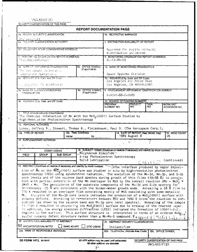
SECURITY CLASSIFICATION OF THIS PAGE
REPORT DOCUMENTATION PAGEla REPORT SECURITY CLASSIFICATION lb. RESTRICTIVE MARKINGS
2a ECuiHiTY CLASSIFICATION AUTHORITY 3. DISTRIBUTION/AVAILABILITY OF REPORT
2b SELA. ICAION DOWNGRADING SCHEDULE Approved for public release;distribution un' inited.
5ERFORY--G O G3AN ZA-ION REPO9T NUMBER(S) 5. MONITORING ORGANIZA1 ION REPORT NUMBERIS)
SD-'1i-89-59
6a PNA E -,E5,OMING ORGANIZArON 6b. OFFICE SYMBOL 7a. NAME OF MONITORING ORGANIZATION""h :;D(cIf: " A>.J (f applicable)
! >v per'a .o.. Spdce Systems Divisionbc AC S , C.lv State and ZIP Code: 7b. ADDRESS (City State, and ZIP Code)
Los Angeles Air Force BaseLos Angeles, CA 90009-2960
1a NAME OF -uINDiG, SPONSORING 8b. OFFICE SYMBOL 9 PROCUREMENT INSTRUMENT IDENTIFICATION NUMBERRGAN1ZATON (I f applicable)I ~F04701 -88-C- 0089
8c ADDRESS (Ci.y. State and ZIP Code) 10. SOURCE OF FUNDING NUMBERSPROGRAM PROJECT TASK WORK UNITELEMENT NO. NO. NO. ACCESSION NO
TITLE (Include Security Classification)
The Chemical Interaction of Mn With the MoS2 (0001) Surface Studied byHigh-Resolution Photoelectron Spectroscopy
12. PERSONAL AUTHOR(S)
Lince, Jeffery R., Stewart, Thomas B., Fleischauer, Paul D. (The Aerospace Corp.);13a TYPE OF REPORT 13b. TIME COVERED 14. CATE CF REPORT (Yea, Month, Day) 15. PAGE COUNT
FROM TO 1989 August 8 126
16 SUPPLEMENTARY NOTATION
7. COSATI CODES 18. SUBJECT TERMS (Continue on reverse if necessa and identify by block number)
FIELD GROUP SUB-GROUP j')lolybdenulm Disulfide-. X-ray Photoelectron Spectroscopy
Solid Lubrication -.. (continued)
19. ABSTRACT (Continue on reverse it necessary and identify by block number) '- The interface produced by vapor deposi-
tion of Mn on the No3'(0001) surface was studied in'situ by high-resolution photoelectronspectroscopy (PES) using synchrotron radiation. The evolution of the Mo-3d, Mn-3p, and S-2pcore levels and of the valence band spectra during growth of thin films 1iO 58 4) is consis-tent with partial conversfoi of the Mn overlayer to MnS by the overall reaction 2Mn VMoS I
2MnS + Mo. The persisterce of the substrate components of the Mo-3d and S-2p spectra forth.cknesses 35 A are consistent with the Volmer-Weber growth mode. Annealing a 58-X film to770 K resulted in an overlayer film consisting mostly of MnS coexisting with some metallicMn. Analysis of the Mo-3d core levels indicates the production of a MoS 2 (0001) surface withvacancy defects. Annaling to temnPrature between 850 and 1040 K drove the reaction to corn-pletion ',as shown by the valence band and Mn-3p core level spectra). Annealing of the sample- 1130 K resulted in uncuvtring the MoS i(0001) surface due to breakup of the reacted iayer.
in addition, low energy electron diffraction (LEED) indicated the formation of (0001 )-2,2,region, on the surf:ice. This surface structure is interpreted in terms of an ordered MoS(,_j'* sulr vcancy defect structure rather than a Mn-Mo-S compound. Ac L&. u
20 DISTRMBfl IONAVAILABILITY OF ABSTRACT | 21. ABSTRACT SECURITY CLASSIpICA:TION
UNCLASSIFIED/UNLIMITED Ei SAME AS RPIT [] DTIC USERS Unclassified
22a NAME OF RESPONSIBLE INDIVIDUAL 22b. TELEPHONt (Include Are Code) 22c. OFFICESYMBOL
DD FORM 1473, 84 MAR 83 APR edtion may be used until exhausted. SECURITY CLASSIFICATION OF THIS PAGEAll oter edlftns are obsolete UNCLASSIFIED
UNCLASSIFIED
SECURITY CLASSIFICATION OF THIS PAGE
12. PERSONAL AUTHOR(S) (Continued)
Yarmoff, Jory A. (National Institute of Standards and Technology); and Taleb-Ibrahimi, Amina(IBM T. J. Watson Research Center).
18. SUBJECT TERMS (Continued)
AdhesionManganeseInterfacial ChemistryMetal/Semiconductor Interfaces
SECURITY CLASSIFICATION OF THIS PAGE
UNCLASSIFIED
PREFACE
This work was supported predominantly by Air Force Systems Command,
Space Systems Division, Contract Number FO4701-85-C-0086. Research was
carried out in part at the National Synchrotron Light Source, Brookhaven
National LAboratory, which is supported by the U. S. Department of Energy,
Divisicn o! Materials Sciences and Division of Chemical Sciences (DOE con-
tract number DE-AC02-76CH00016).
.:c5eai3n For
ByD r ' I- but i ou/
t I. I1ty' Codes
• ................ .
CONTENTS
PREFACE ............................................................. 1
I. INTRODUCTION .................................................. 7
II. EXPERIMENTAL .................................................. 9
III. RESULTS AND DISCUSSION ........................................ 11
A. Core Level Spectra ....................................... 11
B. Valence Band Spectra ..................................... 18
C. Formation of MoS2 (O00i) - 2 . 2 .......................... 20
IV. SUMMARY AND CONCLUSIONS ....................................... 23
REFERENCES .......................................................... 25
• I / I I3
TABLES
I. Binding Energies of Mo-3d and S-2p Core Levels onthe MOS2 (0001) Surface After Mn Deposition .................... 14
If. Relative Areas of the Mo-3d and S-2p Peaks of theMOS2(0001) Surface After Mn Deposition ........................ 15
FIGURES
1. Mo-3d and S-2p Core Level Spectra for Deposition ofMn on the MoS2 (0001) Surface .................................. 12
2. Mn-3p and Mo-4p Core Level Spectra for Depositionand Annealing of Mn on the MoS2(0001) Surface ................. 13
3. Mo-3d and S-2p Core Level Spectra for Annealing ofMn on the MoS2 (0001) Surface .................................. 17
4. Valence Band Spectra for Deposition and Annealingof Mn on the MoS2(0001) Surface ............................... 19
5
I. INTRODUCTION
_The interaction of transition metals with MoS2! surfaces has been
increasingly studied recently with respect to applications in catalysis,
electronics materials,2,3 and tribology (lubricatior) Especially well
studied is the chemistry at the metal/MoS2 (O001) interface. This surface
of MoS 2 is remarkable because of the highly anisotropic MoS 2 crystal struc-
ture. MoS2 crystallizes in layers of S-Mo-S "sandwiches," within which the
bonds are covalent, but each layer is bonded to the next one by relatively
weak van der Waals' forces. As a result, its basal plane [or (0001)] sur-
face, produced by cleaving between these layers, is relatively inert with
respect to metal deposition.
The expected reaction of metals with MoS 2 to form metal sulfides is as
follows:
b 1 bMe + MoS MeS + Mo (1)
2a 2 a ab 2a
The free energy of reaction per metal atom (or AG ) indicates that, atr xn
room temperature, a large number of metals are able to form sulfides based
on bulk, equilibrium thermodynamics.2 ,3 However, the work of McGovern,
et al., 3 Lince, et al. ,2 , and Kamaratos, et al.,1,5,6 indicates that, al
though a negative or small positive AGrx n is a necessary condition for
chemical reaction in this system, it is not sufficient as an indicator of
reactivity at room temperature. Of the metals studied that correspord to
this thermodynamic condition (i.e., are expected to chemically react with
MoS 2 ), Al,2 '3 Cu, 3 In, 2 '3 Pd, 2 '5 and V2 do not react, Fe1, 4 and Ni3 exhibit
minimal reactivity (Ni might be nonreactive),6 and only Mg,2,3 Ti, 2 ,3 andMn2 exhibit strong reactivity, i.e., decomposition of the substrate into
metallic molybdenum and metal sulfide. Therefore, there are kinetic con-
straints in this system due to the structure of the individual metals in
addition to the anisotropic structure of the MoS2(0001) surface.
7
To investigate the chemistry of the more reactive interfaces in
greater detail, we conducted a study of the interaction of thin films of Mn
with the MoS 2 (0001) surface. The techniques we used are (a) core level and
valence band photoelectron spectroscopies excited by synchrontron rad-
iation, and (b) low energy electron diffraction (LEED). The use of syn-
chrotron radiation allows for control of the electrc.: escape depth by vary-
ing the photon energy. In addition, the use of a small line-width mono-
chromator and a high-resolution electron energy analyzer is shown to be
necessary to correctly deconvolute the various species in the core level
spectra, since binding energy shifts can be small during sulfide formation.
8
II. EXPERIMENTAL
The present study was performed at beam line UV-8b at the National
Synchrotron Light Source at Brookhaven National Laboratory. The sample
preparation procedures, 7 electron spectrometer, 8 and monochromator 9 have
been described previously. Briefly, clean basal plane [or (0001)] surfaces
were produced by cleavage of natural molybdenite crystals in air, followed
by annealing at -975 K for 10 min in the metal deposition chamber
(_1 10- 10 Torr base pressure). This annealing procedure is known to
remove virtually all contamination from the surface without formation of
defects. 10,11 Photoelectron spectra showed no evidence of either carbon,
oxygen, or other impurities on the surface of the samples after the anneal,
while LEED showed good quality (0001) - 1 - 1 patterns. The sample
preparation chamber was connected to the spectrometer chamber (-3 - 10- 1 1
Torr base pressure), so that the samples could be kept in ultrahigh vacuum
(UHV) during transfer between metal deposition and analysis steps.
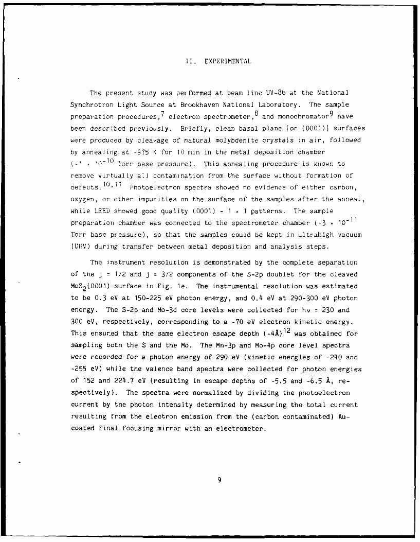
The instrument resolution is demonstrated by the complete separation
of the j = 1/2 and j = 3/2 components of the S-2p doublet for the cleaved
MOS 2 (0001) surface in Fig. le. The instrumental resolution was estimated
to be 0.3 eV at 150-225 eV photon energy, and 0.4 eV at 290-300 eV photon
energy. The S-2p and Mo-3d core levels were collected for hv = 230 and
300 eV, respectively, corresponding to a -70 eV electron kinetic energy.
This ensur.ed that the same electron escape depth (-4A) 12 was obtained for
sampling both the S and the Mo. The Mn-3p and Mo-4p core level spectra
were recorded for a photon energy of 290 eV (kinetic energies of -240 and
-255 eV) while the valence band spectra were collected for photon energies
of 152 and 224.7 eV (resulting in escape depths of -5.5 and -6.5 A, re-
spectively). The spectra were normalized by dividing the photoelectron
current by the photon intensity determined by measuring the total current
resulting from the electron emission from the (carbon contaminated) Au-
coated final focusing mirror with an electrometer.
9
"ore [evel spectra were deconvoluted with Voigt functions ising a peak
fitting procedure. The Mo-3d doublet was fit by constraining the peak
separatior, and the branching ratio for the 5/2 and 3/2 spin-orbit compo-
nents to be 3. 14 eV and 1.43, respectively, while the corresponding con-
straints for the S-2p 3/2 and 1/2 spin-orbit components were 1.19 eV and
2.01. These values were derived from spectra for a number of clean
MoS2 (000') surfaces (The branching ratios are different from the theoreti-
cal values of 1.50 and 2.00 due to final state effects.)
Manganese (99.995% purity) was evaporated onto the sample surface from
a 1/4-in.-diameter tungsten wire basket at a rate of -12 A/min. The pres-
sure during deposition was typically in Lhe mid 10- 10 Torr range. The
sample remained at ambient temperature during deposition. Mn film thick-
nesses were determined by measuring the deposition rate with a quartz crys-
tal microbalance, which could be moved into the position where the sample
is located during film growth. This procedure is accurate to within -50%.
After the deposition, and also after subsequent annealing, there was no
evidence of carbon or oxygen detected by photoelectron spectroscopy.
The deposition of Mn and subsequent annealing was performed on two
separate samples. The spectra displayed herein are from one sample, but
are also representative of those for the other sample.
10
ill, RESULTS AND DISCUSSION
A. CORE LEVEL SPECTRA
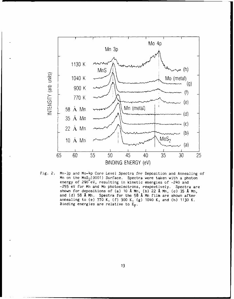
Figure 2 shows the evolution of the Mn-3p and Mo-4p core levels
deposition of Mn on MoS 2 (0001 ) and subsequent annealing. As the Mn is
derpsited, the Mn peak increases relative to the Mo peak. The Mn film has
covered the MoS 2 substrate after deposit' n of 58 A Mn (the Mo-4p is pre-
sent in Fig. 2c, but is difficult to see because of the high relative in-
tensity of the Mn-3p peak). The binding energy and the increased intensity
on the high binding energy side of the Mn-3p peak for all coverages indi-
cates that the Mn is primar'ly in the form of metallic Mn coexisting with a
small amount of Mn in a higher oxidation state, possibly as a sulfide.
Annealing the 58 A film to progressively higher and higher temperatures
results in reappearance of the Mo-4p peak caused by agglomeration of the Mn
layer into islands, which uncovers the substrate. In addition the Mn-3p
spectrum shifts -1.8 eV to higher binding energy with the first anneal, and
exhibits a decrease in overall peak width. This shift is consistent with
the formation of MnS, since the difference in the Mn-3p binding energies of
Mn and MnS has been determined to be in the range of 1.6 eV13'14 to
2.4 eV. 15 Therefore, the increase in temperature increased the rate of
reaction, driving the reaction to equilibrium, which in this case corres-
ponds to sulfide formation, consistent with the negative AG mentionedrxnabove. After the anneals, the Mo-4p spectrum appears to have shifted to
lower binding energy, indicating reduction of the Mo in the MoS 2.
The various species in the Mo-3d and S-2p spectra were deconvoluted by
curve fitting, and the results are shown ;n Fig. 1 for the clean surfaces
and three of the depositions (22, 35, and 58 X; the corresponding spectra
for 10 and 50 A are not shown for reasons of brevity, but their trends are
similar to the spectra shown). Initial deposition of Mn caused the Mo-3d
peak representing the Mo in the MoS2 substrate [Mo in the +4 oxidation
state, denoted "Mo(substrate)"] to shift -0.3 eV to lower binding energy
11
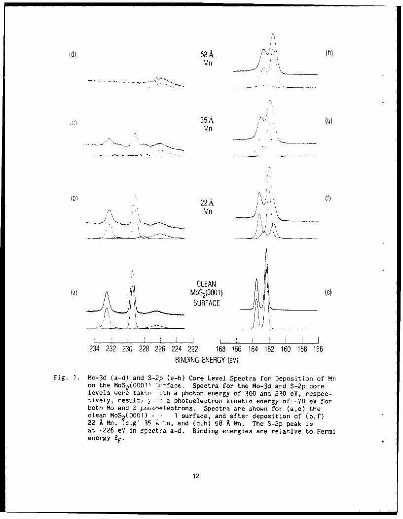
(d) 58 A N f (h)Mn/
iC) 35A 7"- (g)Mn
(0 22A (f)
,' "1 Mn \
" P" ItCLEAN
(a) A MOS2(0001) (e)SURFACE
____, ___ ____ ____ I I234 232 230 228 226 224 222 168 166 164 162 160 158 156
BINDING ENERGY (eV)
Fig. 1. Mo-3d (a-d) and S-2p (e-h) Core Level Spectra for Deposition of Mnon the MoS 2(0001) ",,face- Spectra for the Mo-3d and S-2p corelevels were tak,.r ith a photon energy of 300 and 230 eV, respec-tively, result, in a photoelectron kinetic energy of -70 eV forboth Mo and S pnrocnelectrons. Spectra are shown for (a,e) theclean MoS (0001) - 1 surface, and after deposition of (b,f)22 A Mn, fc,g' 35 ,s .n, and (d,h) 58 A Mn. The S-2p peak isat -226 eV in Zectra a-d. Binding energies are relative to Fermienergy EF.
12
Mo 4p
Mn 3p
1130 K I
1040 K Mo (metal)900 K
_770 K
LU 58 n35 ,%.Mn(d)
35 A Mn
22 X Mn (
10 X Mn MoS2(a)
65 60 55 50 45 40 35 30 25BINDING ENERGY (eV)
Fig. 2. Mn-3p and Mo-4p Core Level Spectra for Deposition and Annealing ofMn on the MoS2 (0001) Surface. Spectra were taken with a photonenergy of 290 eV, resulting in kinetic energies of -240 and-255 eV for Mn and Mo photoelectrons, respectively. Spectra areshown for depositions of (a) 10 A Mn, (b) 22 A Mn, (c) 35 A Mn,and (d) 58 A Mn. Spectra for the 58 A Mn film are shown afterannealing to (e) 770 K, (f) 900 K, (g) 1040 K, and (h) 1130 K.Binding energies are relative to EF.
13
due to band-bending (see Fig. lb and Table I). Also, a reduced Mo species
znoears whose separation from the Mo(substrate) peak (-1.0 eV, see Table I)
corresponds with the formation of metallic Mo [denoted Mo(metal)]. 13 The
S-2p spectrum deconvolutes clearly into two species (see Fig. If): the
substrate S [denoted S(substrate) in Table I, and a lower-binding energy
species show binding energy (BE) is consistent with that for MnS15 ,16 [de-
noted S(MnS)]. The Mo(metal) peak and the S(MnS) peaks increase in area
(relative to the substrate peaks, see Table II) with deposition up to
35 A thickness (see Fig 1, spectra c and g). For the 58 A deposition, Mo
is not detectable above the noise level in the Mo-3d region (see Fig. Id),
and the S-2p peak exhibits mostly a broadened peak representing the MnS,
with a small amount of intensity on the high binding energy side, possibly
representing a small amount of S from the MoS 2 substrate (see Fig. lh).
Table I. Binding Energies of Mo-3d and S-2p Core Levels on theMOS 2 (0001) Surface After Mn Depositiona
Mo-3d S-2p
BE BE BE BE
Mo(substrate) Mo(metal) S(substrate) S(Mns)
Clean surface 229.4 eV --- 162.3 ---
Average for 10, 22, 229.07 228.04 161.93 161.40
and 35 A Mn t.03 ±.08 ±.06
770 K anneal 228.45 227.68 161.64±.10
Average for --- 227.90 --- 161.55850, 900, 970 ±.05 ±.06and 1040 K anneals
1130 K anneal 229.18 227.82 161.94 161.25±.05 ±.10
auncertainty in binding energies is -0.02 eV, unless otherwise stated.
14
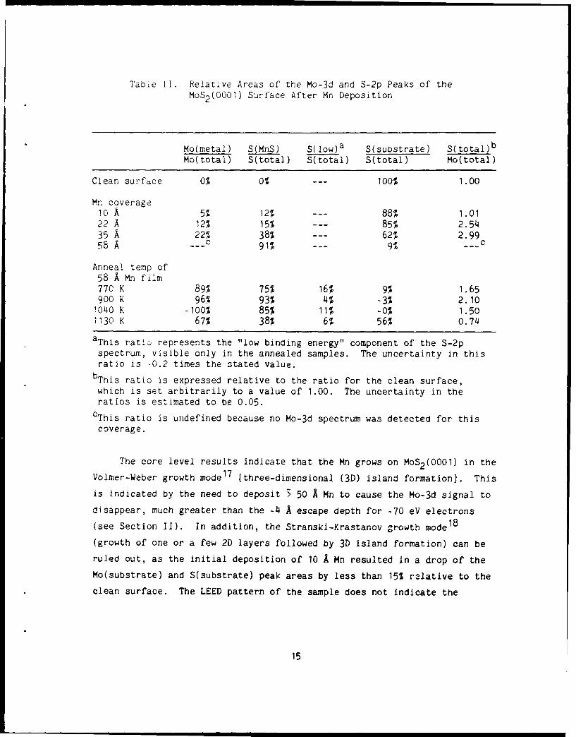
Table 11. Relative Areas of the Mo-3d and S-2p Peaks of theMOS 2 (0001) Surface After Mn Deposition
Mo(metal) S(MnS) S(low)a S(substrate) S(total)b
Mo(total) S(total) S(total) S(total) Mo(total)
Clean surface 0% 0% 100% 1.00
Mn coverage10 A 5% 12% --- 88% 1.0122 A 12% 15% --- 85% 2.5435 A 22% 385 --- 62% 2.9958 A -_c 91% --- 9% __ c
Anneal temp of58 A Mn film77C K 89% 755 16% 9% 1.65900 K 96% 93% 4% -3% 2.101040 K -100% 85% 11% -0% 1.501130 K 67% 38% 6% 56% 0.74
aThis ratio represents the "low binding energy" component of the S-2pspectrum, visible only in the annealed samples. The uncertainty in thisratio is -0.2 times the stated value.
bThis ratio is expressed relative to the ratio for the clean surface,
which is set arbitrarily to a value of 1.00. The uncertainty in theratios is estimated to be 0.05.
CThis ratio is undefined because no Mo-3d spectrum was detected for this
coverage.
The core level results indicate that the Mn grows on MoS2 (0001) in the
Volmer-Weber growth mode 17 [three-dimensional (3D) island formation). This
is indicated by the need to deposit ) 50 A Mn to cause the Mo-3d signal to
disappear, much greater than the -4 A escape depth for -70 eV electrons(see Section I). In addition, the Stranski-Krastanov growth mode 18
(growth of one or a few 2D layers followed by 3D island formation) can be
ruled out, as the initial deposition of 10 A Mn resulted in a drop of the
Mo(substrate) and S(substrate) peak areas by less than 15% relative to the
clean surface. The LEED pattern of the sample does not indicate the
15
presence of an ordered overlayer f_1m, since de?'sition of 10, 22, and
35 A Mn causes an increase in background intensity of the (0001) - 1 - 1
pattern, wrile for dispositions of 50 and 58 A Mn, and anneals of 770-1040 K, no pattern is seen at all.
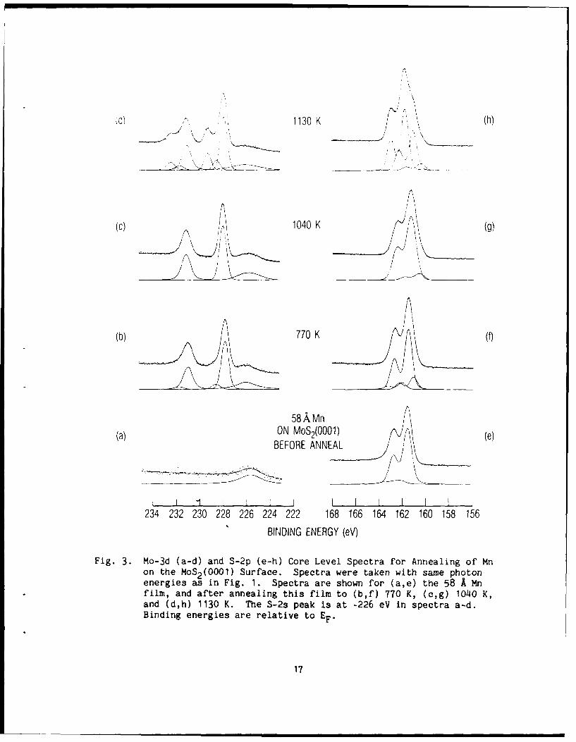
After annealing the 58 A film to 770 K, the Mo-3d spectrum reappears
(see Fig. 3t). This deconvolutes into two doublets. The larger one cor-
responds to the binding energy for metallic Mo, 13 although it is -0.2 eV
less than for the subsequent anneals to 850 - 1040 K. The smaller doublet
corresponds well to MoS 2 with S vacancy defects, or MoS2 _x, where
0 < x " 1.7 The S-2p doublet (see Fig. 3f) represents mainly MnS, but
exhibits a small amount of intensity on the high binding energy side, pos-
sibly corresponding to S in the MoS 2_x region of the surface, and a lower
binding energy species. This lower binding energy species [denoted S(low)
in Table II might represent another sulfide of Mn. It also might
represent S adsorbed on the surface of either the Mo(metal) or the MnS.
(The adsorption of S on Mo(0001) has been shown to exhibit a lower S-2p
binding energy than S in MoS 27,19.) When the sample is annealed to higher
temperatures, i.e., to 850 and 900 K, the substrate components in both the
Mo-3d and S-2p spectra decrease (see Table I), and have disappeared after
the anneal to 970 and 1040 K (see Table II and Fig. 3, spectra c and g).
This indicates that the reaction to form MnS has been driven by the
increase in temperature, in agreement with the Mn-3p core level results
(see Fig. 2, spectra d through g). The decrease in the area of the S(low)
doublet at 850 K and 900 K is concurrent with the rise in the
S(total):Mo(total) ratio, while the subsequent rise in S(low) at 970 K and
1040 K is concurrent with the fall of the S(total):Mo(total) ratio. The
amount of Mo(total) is virtually equal to the amount of Mo(metal) during
annealing. Therefore, a change in the amount of S(low) seems to move in
the same direction as a change in the amount of Mo(metal). This is
consistent with the conclusion that the S(low) species represents S
adsorbed on the Mo(metal).
16
d) .1130 K / (h)
(c) 1040 K (g)(c) iNN ',//
(b) 770K ()
58 ,k Mn(a) ON MOS 2(0001) (e)
BEFORE ANNEAL
-.......
I I I I I I I I I234 232 230 228 226 224 222 168 166 164 162 160 158 156
BINDING ENERGY (eV)
Fig. 3. Mo-3d (a-d) and S-2p (e-h) Core Level Spectra for Annealing of Mnon the MoS2(0001) Surface. Spectra were taken with same photonenergies as in Fig. 1. Spectra are shown for (a,e) the 58 A Mnfilm, and after annealing this film to (b,f) 770 K, (c,g) 1040 K,and (d,h) 1130 K. The S-2s peak is at -226 eV in spectra a-d.Binding energies are relative to EF.
17
The drop in the Mo(metal) peak area as the annealing temperature is
increased from 7!0 K to 900 K is due to continued MnS formation (see
Section III-B, below), which competes with the Mo(metal) for coverage of
the surface. The loss of some of the adsorbed S at this point may also be
related to the formation of MnS. The increase in the Mo(metal) peak area
between 900 K and 1040 K may be due to partial decomposition of the MnS,
which serves as a source for the return of the adsorbed S. S adsorbed on
Mo is relativ,.ly refractory19 and, therefore, would not be desorbed at this
temperature.
B. VALENCE BAND SPECTRA
Valence band photoelectron spectra were taken for photon energies of
152 eV and 225 eV during depositon of Mn on MoS2 (0001) and subsequent
annealing of the samples. Only the 152 eV spectra are reproduced here (see
Fig. 4), since the results of the two sets show good agreement. Initial
deposition causes shifting of the spectrum -0.3 eV to lower binding energy
(see Fig. 4b), in agreement with the band-bending seen in the core
levels. Also, increased intensity from I eV to the Fermi level indicates
that the surface is becoming metallic due to the presence of metallic Mn.
The MoS2 peak structure is still seen in the 10 A spectrum, showing that
the substrate has not reacted appreciably or been covered by the over-
layer. Also, when the metallic edge of the 10 A spectrum is scaled to
coincide with the corresponding metallic edge of the 35 A spectrum, and the
35 A spectrum is subtracted from the 10 A spectrum, the resultant differ-
ence spectrum is virtually identical to that for the clean surface, indi-
cating that the reacted layer (i.e., Mn+MnS+Mo) coexists with relatively
undisturbed substrate. Therefore, probably no MnxMoS2 compound is formed
during deposition. Spectra c and d in Fig. 4 (especially d) correspond
well with the valence band spectrum for Mn metal. 15 The 35 A spectrum
(Fig. 4c) exhibits a bit more intensity in the areas of -4 eV and -6 eV
than the 58 A spectrum (Fig. 4d). This is due to the persistence of the
signal from the substrate (compare Fig. 2, spectra c and d).
18
MnS-.
1040 K(h) 970 K
~(g)900 K
,a 850 K
)Mn 770 KANNEAL
E (d)
(C) 58 A Mn
(b) 35A Mn
10A Mn(a) CLEAN MoS 2
20 15 10 5 0 -5 -10BINDING ENERGY (eV)
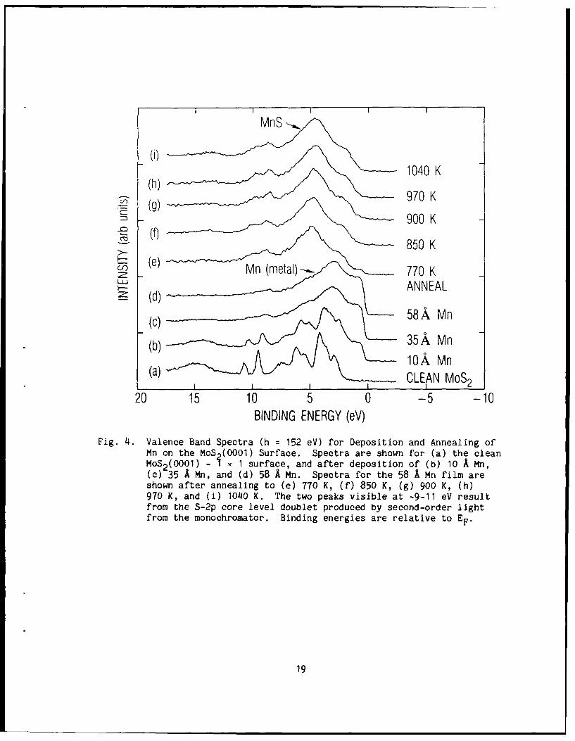
Fig. 4. Valence Band Spectra (h = 152 eV) for Deposition and Annealing ofMn on the MoS (0001) Surface. Spectra are shown for (a) the cleanMOS2 (0001) - i x 1 surface, and after deposition of (b) 10 A Mn,(c) 35 A Mn, and (d) 58 A Mn. Spectra for the 58 A Mn film areshown after annealing to (e) 770 K, (f) 850 K, (g) 900 K, (h)970 K, and (i) 1040 K. The two peaks visible at -9-11 eV resultfrom the S-2p core level doublet produced by second-order lightfrom the monochromator. Binding energies are relative to EF.
19
With the anneal to 770 K (see Fig. 4e), a large increase in intensity
appears at -5 eV, due to the formation of MnS (see below) and the reappear-
ance of the substrate. Also, the Mn metal areas of the valence band (at -1
and -3 eV) persist, indicating that there is a small amount of unreacted Mn
at this annealing temperature. After annealing to 850 K, however, there is
no evidence for the existence of unreacted Mn (see Fig. 4f). The spectra
for anneals between 850 and 1040 K indicate a mixture of MnS (represented
mainly by the peak at -.5 eV15'16 ) and metallic Mo (peak at -2 eV2 0 ), in
agreement with the core level spectra (see Fig. 2, spectra f and g; also
Fig. 3, spectra c and g). The MnS peak shifts -0.5 eV to lower binding
energy as the temperature is increased from 900 K to 1040 K. This may be
due to a phase transition in MnS from the a phase to the a phase2 1 or
partial decomposition, as mentioned above.
C. FORMATION OF MoS 2 (0001) - 2 - 2
After annealing to 1130 K, the substrate (0001) - 1 1 1 LEED pattern
reappeared, and also exhibited half-order spots over much of the sample
surface, indicating the formation of a surface structure with (0001)
2 x 2 periodicity. In addition, the core level spectra exhibit large
changes in shape (see Fig. 3, spectra d and h). The Mo-3d and S-2p core
levels can be deconvoluted into three doublets each. The Mo-3d spectrum
(see Fig. 3d) exhibits the reappearance of the Mo(substrate) doublet
resulting from MoS2 , coexisting with a large Mo(metal) doublet. In
addition, a smaller doublet appears with a binding energy intermediate
between these two doublets, which probably represents the 2 x 2 regions of
the surface. The S-2p doublet deconvolutes into a large substrate doublet,
followed at lower binding energies by a slightly smaller S(MnS) doublet,
and a small, lower binding energy doublet. As mentioned above, this lower
binding energy doublet might represent adsorbed S, or it might represent S
in the 2 x 2 regions of the surface.
Preliminary studies involving the thermal decomposition of the
MOS2 (0001) - 1 1 1 surface2 2 correlate well with the present results.
Annealing to temperatures in excess of 1375 K caused the formation of a
20
(0001) - 2 - 2 LEED pattern, similar to annealing the Mn/MoS 2(0001)
interface to 1130 K in the present study. In addition, the core-level
photoelectron spectra of the annealed MoS 2 (0001) surface appear similar to
those of the annealed Mn/MoS 2(O001) interface.
In a recent study of the Fe/MoS 2(0001) interface,I a (0001) - 2 x 2
LEED pattern was observed when the sample was annealed to 1200 K. This re-
sult, the results of the present study, and the preliminary thermal decom-
position results for the clean surface, indicate that the (0001) - 2 x 2
LEED pattern seen for higher temperature-annealed metal/MoS2 interfaces is
not due to the formation of a (metal)xMOS2 compound, but rather is due to
sulfur vacancy defects in the surface region, produced when the metals
react with the MoS2 to form metal-sulfur compounds. Therefore, these
chemically produced defects allow the (0001) - 2 x 2 structure to form at a
lower temperature than for the clean surface. In addition, the difference
in reactivity between Fe and Mn affects the formation of this structure.
Although Fe exhibits some evidence of reactivity with respect to
MOS 2 (0001),I,4 the reactivity is considerably less than for Mn on
MOS 2 (0001).2 Since there is less deficiency of S in the substrate surface
for Fe/MoS2 , a higher temperature (1200 K) is required to produce the
(0001) - 2 - 2 defect structure than for Mn (1130 KO.
Although valence band spectra for the 1130 K anneal were not taken
with a 152 eV photon energy as in Fig. 4, a spectrum with a 225 eV photon
energy (not shown) was taken that exhibits a broad peak with maximum
intensity at -4.5 eV, and higher intensity at -2 eV than in the previous
spectra. The general shape of the spectrum indicates that Mo(metal) and
MnS continue to cover some of the surface, with a broad structureless
valence band shape indicating disorder in the uncovered areas of the sur-
face that contributed to the (0001) - 1 x 1 and - 2 x 2 LEED patterns.
21
IV. SUMMARY AND CONSLUSIONS
A core level and valence band photoelectron spectroscopy study was
conducted of the Mn/MoS 2 (0001) interface. In general, it was shown that Mn
reacted with the MoS 2(0001) surface as represented in the overall reaction:
1 1Mn + 1 MoS - MnS + - Mo (2)2 2 2
Specifically, Mn forms three-dimensional islands on MoS2 , covering the
substrate with a complete layer only for an amount of Mn that would have
given a thickness equivalent to -50 A for layer-by-layer deposition. Re-
action (2) initiated for thicknesses K 10 A Mn, and was driven by increas-
ing amounts of Mn. The binding energies of the deposition-produced species
in the Mn-3p and S-2p core level spectra corresponded to MnS, while the
Mo-3d spectra indicated the formation of metallic Mo. Valence band spectra
showed that for initial deposition, the partially reacted layer (i.e.,
Mn+MnS Mo) formed an abrupt interface with the unreacted substrate.
The reaction was driven by annealing -50 to -58 A Mn films on
MoS2 (0001) to temperatures in the range 770 - 1040 K. Analysis of the core
levels after annealing to 770 K indicated that the MoS2 substrate surface
was sulfur-deficient, while valence band spectra showed that some unreacted
Mn coexisted with a mostly MnS overlayer. The reaction was driven to com-
pletion by annealing to temperatures 850 K.
Annealing to temperatures 3 1130 K resulted in the formation of a
MoS2 (O001) - 2 - 2 LEED pattern. The observation of this surface structure
is interpreted in terms of a sulfur-vacancy-produced defect structure,
rather than a metal-Mo-S compound.
23
REFERENCES
1. M. Kamaratos, and C. A. Papageorgopouios, Surf. Sci. 160, 451 (1985).
2. J. R. Lince, D. J. Carre, and P. D. Fleischauer, Phys. Rev. B. 36,16247 (1987).
3. I. T. McGovern, E. Dietz, H. H. Rotermund, A. M. Bradshaw, W. Braun,W. Radlik, and J. F. McGilp, Surf. Sci. 152/153, 1203 (1985).
4. J. R. Lince, T. B. Stewart, M. M. Hills, P. D. Fleischauer, J. A.Yarmoff, and A. Taleb-Ibrahimi, Surf. Sci. (submitted).
5. M. Kamaratos, and C. A. Papageorgopoulos, Appl. Surf. Sci, 29, 279(1987).
6. C. A. Papageorgopoulos and M. Kamaratos, Surf. Sci. 164, 353 (1985).
7. J. R. Lince, T. B. Stewart, M. M. Hills, P. D. Fleischauer, J. A.Yarmoff, and A. Taleb-lbrahimi, Surf. Sci. 210, 387 (1989).
8. D. E. Eastman, J. J. Donelon, N. C. Hein, and F. J. Himpsel, Nucl.Inst. Meth. 172, 327 (1980).
9. F. j. Himpsel, Y. Jugnet, D. E. Eastman, J. J. Donelon, D. Grinmn, G.Landgren, A. Marx, J. F. Morar, C. Oden, and R. A. Pollak, Nucl.Instrum. Meth. 222, 107 (1984).
10. J. C. McMenamin and W. E. Spicer, Phys. Rev. B 16, 5474 (1977).
11. J. Bandet, A. Malvand, and Y. Quemener, J. Phys. C 13, 5657 (1980).
12. Calculated from formula in S. Tanuma, C. J. Powell, and D. R. Penn,Surf. Sci 192, L849 (1987), which was for electron kinetic energies of200 eV and higher.
13. C. D. Wagner, W. M. Riggs, L. E. Davis J. F. Moulder, and G. E.Muilenberg, eds., X-ray Photoelectron Spectroscopy (Perkin-Elmer, EdenPrairie, 1979).
14. H. F. Franzen, M. X. Umana, J. R. McCreary, and R. J. Thorn, J. Solid
State Chem. 18, 363 (1976).
15. H. F. Franzen, and C. Sterner, J. Solid State Chem. 25, 227 (1978).
16. H. van der Heide and C. F. van Bruggen, Mater. Res. Bull. 17, 1517(1982).
25

17. M. Volmer and A. Weber, Z. Phys. Chem. 119, 277 (1926).
18. I. N. Stranski and L. Krastanov, Acad. Wiss. Math.-Nat. KI lib 146,797 (1938).
19. A. Gellman, W. T. Tysoe, F. Zaera, and G. A. Somorjai, Surf. Sci. 191271 (1987).
20. S. J. Atkinson, C. R. Brundle, and M. W. Roberts, Chem. Phys. Lett.24, 175 (1974).
2'. M. Hansen, Constitution of Binary Alloys (McGraw-Hill, New York,1958), p. 950.
22. J. . nce (unpublished results).
26
LABORATORY OPERATI(NS
The Aoro;pace Corporat ron functions as an "architect -engineer" for
ion.i security projects, -iecializing in advanced military space systems.
I:,viding research support, the corporation's Laboratory Operations conducts
experimental and theoretica: investigations that focus on the application of
scientific and technical advances to such systems. Vital to the success of
these Iiwestigations is the 'echnical staff's wide-ranging expertise and its
ability to stay current with new developments. This expertise is enhanced by
a research program aimed at dealing with the many problems associated with
rapidly evolving space systems. Contributing their capabilities to the
research effort are these .ndividual laboratories:
Aerophysics Laboratory: Launch vehicle and reentry fluid mechanics, hea.transfer and flight dynamics; chemical acd electric propulsion, propellantchemistry, chemical dynam , environmental chemistry, trace detection;spacecraft structural me( anics, contamination, thermal and structuralcontrol; h!gh temperaturt: thermomechanics, gas kinetics and radiation; cw andpulsed chemical and exciier laser development including chemical kinetics,spectroscopy, optical resonators, beam control, atmospheric propagation, lasereffects and countermeasures.
Chemistry and Physi-, Laboratory: Atmospheric chemical reactions,atmospheric optics, light scattering, state-specific chemical reactions andradiative signatures of t<ssile plumes, sensor out-of-field-of-view rejection,applied laser spectroscc y, laser chemistry, laser optoelectronics, solar cellphysics, battery electr :hemistryi-space vacuum and radiation effects onmaterials, lubrication , I surface phenomena, thermionic emission, photo-sensitive materials and detectors, atomic frequency standards, andenvironmental chemistry.
Computer Science Laboratory: Program verification, program translation,performance-sensitive system design, distributed architectures for spacebornecomputers, fault-tolerant computer systems, artificial intelligence, micro-electronics applications, communicazion protocols, and computer security.
Elictronics Research Laboratory: Microelectronics, solid-state devicephysics, compound semiconductors, radiation hardening; electro-optics, quantumelectronics, solid-st. lasers, optical propagation and communications;microwave semiconductor devices, ;microwave/millimeter wave measurements,diagnostics and radiometry, microwave/millimeter wave thermionic devices;
atomic time and frequency standards; antennas, rf systems, electromagneticpropagation phenomena, space communication systems.
Materials -iences Laboratory: Development of new materials: metals,alloys, cer , polymers and their composites, and new forms of carbon; non-destructive ev, aation, componnt failure analysis and reliabiltty; fracturemechanics and L-ress corrosion; analysis and evaluation of materials at
cryogenic and ilevated temperatures as well as in space and enemy-inducedenvironment3.
Space Sc nges Laboratory: Magnetospheric, auroral and cosmic rayphycics, wave article interactions, magnetospheric plasma waves; atmosphericand ionospheri: physics, density and composition of the upper atmosphere,remote sensing using atmospheric radiation; solar physics, infrared astronomy,infrared sign. tur. anslysi': effects of solar activity, magnetic storms andnuclear explo ions on the earth's atmosphere, ionosphere and magnetosphere;effects of el-ctromagnetic and particulate radiations on space systems; spaceinstrumontaticn.