Tutorial · chr is top h.l ien au @ un io lde nb ur g.d e ...
67
Breaking the diffraction limit: Analysis of diode lasers by nearfield scanning optical microscopy (NSOM) Jens W. Tomm a and Christoph Lienau b a MaxBornInstitut für Nichtlineare Optik und Kurzzeitspektroskopie Berlin, MaxBornStr. 2 A, D12489 Berlin, Germany b Institut für Physik, Fk. V, Carl von Ossietzky Universität Oldenburg Ammerländer Heerstraße 114118, D26129 Oldenburg, Germany [email protected] WWW.BRIGHTER.EU Tutorial 1 WWW.BRIGHTER.EU Plenary Meeting at Tyndall, Cork 2008
Transcript of Tutorial · chr is top h.l ien au @ un io lde nb ur g.d e ...

Breaking the diffraction limit: Analysis of diode lasers by nearfield scanning
optical microscopy (NSOM)
Jens W. Tomm a and Christoph Lienau b
a MaxBornInstitut für Nichtlineare Optik und Kurzzeitspektroskopie Berlin, MaxBornStr. 2 A, D12489 Berlin, Germany
b Institut für Physik, Fk. V, Carl von Ossietzky Universität Oldenburg Ammerländer Heerstraße 114118, D26129 Oldenburg, Germany christoph.lienau@unioldenburg.de
WWW.BRIGHTER.EU Tutorial
1 WWW.BRIGHTER.EU Plenary Meeting at Tyndall, Cork 2008

Outline
1. Introduction NSOM = Nearfield Scanning Optical Microscopy Principles and opportunities Spatial resolution
2. Methodology Laser emission, spontaneous emission and PL
3. NOBIC = Nearfield Optical Beam Induced Current 4. Experimental setups and equipment 5. Analysis of waveguides and determination of mode profiles 6. VCSEL 7. Surface recombination velocity at facets 8. Defect creation during device operation 9. Summary 10. Acknowledgement
2 WWW.BRIGHTER.EU Plenary Meeting at Tyndall, Cork 2008

Introduction
10 µm 1 µm 100 nm 10 nm 1 nm 0.1 nm
Farfield Optical Microscopy
NearField NanoOptics
Semiconductor Nanostructures
...
Nanostructures and Nanoanalytical Tools
Optoelectronic devices
3 WWW.BRIGHTER.EU Plenary Meeting at Tyndall, Cork 2008

Scanning probe microscopy
Disc players for atoms
Compare: If 1 atom had the size of an orange, the cantilever would be 100 km long
Introduction
4 WWW.BRIGHTER.EU Plenary Meeting at Tyndall, Cork 2008

1ns
100 pm
1 nm
10 nm
100 nm
1 µm
10 µm
100 µm
10ps 100ps 1ps 100fs 1fs Time 10fs
Space
Electronic motion in semiconductor nanostructures
Quantum transport
Energy transport in polymers + large biomolecules
Physical phenomena happen on ultrashort length and time scales
Electronic motion in atoms + molecules
Nuclear motion in molecules
Surface plasmon dynamics in metallic nanostructures
Introduction
5 WWW.BRIGHTER.EU Plenary Meeting at Tyndall, Cork 2008

1ns
100 pm
1 nm
10 nm
100 nm
1 µm
10 µm
100 µm
10ps 100ps 1ps 100fs 1fs Time 10fs
Space
Ultrafast nanoscale physics: Imaging tools
Ultrafast nanooptics
Electron microscopy Cathodoluminescence
Ultrafast farfield optical microscopy
Introduction
6 WWW.BRIGHTER.EU Plenary Meeting at Tyndall, Cork 2008

Intensity Sum
Spot 2 Spot 1
x 0.61 / N.A. λ ∆ ≈ Rayleigh limit:
The resolution in optical microscopy is limited by the wavelength of light
Introduction
7 WWW.BRIGHTER.EU Plenary Meeting at Tyndall, Cork 2008

Intensity Sum
Spot 2 Spot 1
x 0.61 / N.A. λ ∆ ≈ Rayleigh limit:
The resolution in optical microscopy is limited by the wavelength of light
Introduction
8 WWW.BRIGHTER.EU Plenary Meeting at Tyndall, Cork 2008

Breaking the resolution limit in microscopy Nearfield scanning optical microscopy
Diffractionunlimited resolution
Introduction
9 WWW.BRIGHTER.EU Plenary Meeting at Tyndall, Cork 2008

Spatial resolution in nearfield microscopy
Electromagneticfield distribution: superposition of monochromatic plane waves:
E E ik r i t = − 0 0 exp( ) exp( ) r r ω = + − E i k x k y ik z i t x y z 0 exp( ( )exp( )exp( ) ω
k k k k k x y z 0 0 2 2 2 = = + +
r
for given k k x y , : two solutions:
(a) propagating waves:
(b) evanescent waves:
k k k k lat x y = + < 2 2 0 k real z .
k k k k lat x y = + > 2 2 0
k imaginary z .
Consequence: Intensity of evanescent waves decreases exponentially with increasing z
How to get optical superresolution ?: ∆ ∆ k x x ≥ 1
Use evanescent modes!
Introduction
10 WWW.BRIGHTER.EU Plenary Meeting at Tyndall, Cork 2008
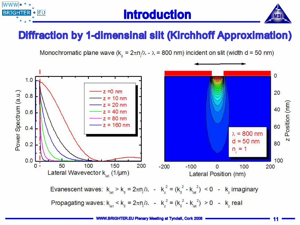
Diffraction by 1dimensional slit (Kirchhoff Approximation)
Introduction
Diffraction by 1dimensinal slit (Kirchhoff Approximation)
11 WWW.BRIGHTER.EU Plenary Meeting at Tyndall, Cork 2008

0 50 100 150 200 0.0
0.2
0.4
0.6
0.8
1.0
Diffraction by 1Dimensional Slit (Kirchhoff Approximation)
z =0 nm z = 10 nm z = 20 nm z = 40 nm z = 80 nm z = 160 nm
Powe
r Spectrum (a
.u.)
Lateral Wavevector k lat (1/µm) 200 100 0 100 200
100
80
60
40
20
0
λ = 800 nm d = 50 nm n r = 3.4
z Position (nm)
Lateral Position (nm)
Monochromatic plane wave (k 0 = 2πn r /λ λ = 800 nm) incident on slit (width d = 50 nm)
Propagating waves: k lat < k 0 = 2πn r /λ k z 2 = (k 0
2 k lat 2 ) > 0 k z real
Evanescent waves: k lat > k 0 = 2πn r /λ k z 2 = (k 0
2 k lat 2 ) < 0 k z imaginary
Diffraction by 1dimensinal slit (Kirchhoff Approximation)
Introduction
12 WWW.BRIGHTER.EU Plenary Meeting at Tyndall, Cork 2008
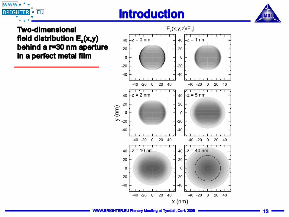
0 20 40
0
20
40 z = 0 nm
40 20 0
40
20
0 0
20
40
|E x (x,y,z)/E 0 |
z = 1 nm
40 20 0
40
20
0
0 20 40
0
20
40
y (nm)
z = 2 nm
0 20 40 40 20 0
40
20
0 0
20
40 z = 5 nm
0 20 40 40 20 0
40
20
0
0
20
40 z = 10 nm
0 20 40 40 20 0
40
20
0
0 20 40
x (nm) 40 20 0
40
20
0 0
20
40 z = 40 nm
Twodimensional field distribution E x (x,y) behind a r=30 nm aperture in a perfect metal film
Introduction
13 WWW.BRIGHTER.EU Plenary Meeting at Tyndall, Cork 2008
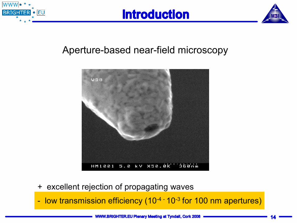
Aperturebased nearfield microscopy
+ excellent rejection of propagating waves
low transmission efficiency (10 4 10 3 for 100 nm apertures)
Introduction
14 WWW.BRIGHTER.EU Plenary Meeting at Tyndall, Cork 2008
Aperturebased nearfield microscopy
Introduction
15 WWW.BRIGHTER.EU Plenary Meeting at Tyndall, Cork 2008

Nearfield Reflectance Spectroscopy with Uncoated Fiber Probes
Illumination/Collection Mode
1000 500 0 0.0
0.2
0.4
0.6
0.8
1.0
Reflectance (a
.u.)
Distance (nm)
Transmission efficiency close to 1 Extremely high collection efficiency
Sensitive probing of nearfield reflectance
Resolution down to λ/5 (150 nm)
Experiment: F. Intonti et al, PRL 87, 076801 (2001), PRB 63, 075313 (2001) Theory: R. Müller and C. Lienau, Appl. Phys. Lett. 76, 3367 (2000).
Introduction
16 WWW.BRIGHTER.EU Plenary Meeting at Tyndall, Cork 2008

2 1 0 1 0
2
4
6
2
4
6
Propagation through Uncoated Fiber Probes
1.0 0.5 0.0
40fs
2 1 0 1 2 2
4
6
z exit
Y (µm)
Y (µm)
52fs
Z(µm
)
z = z exit
|Ê x | 2
/A 0 2
260nm
1 0 1 2
z = z exit +25nm
285nm
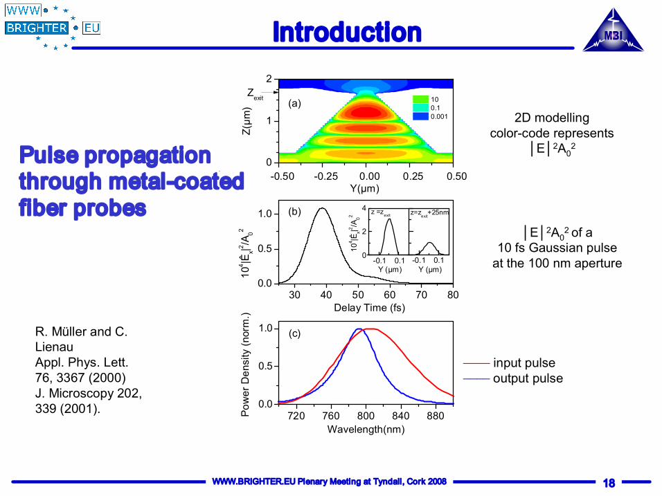
R. Müller Appl. Phys. Lett. 76, 3367 (2000) and J. Microscopy 202, 339 (2001).
Pulse propagation through uncoated fiber probes
2D modelling colorcode represents │E│ 2 A 0 2
Introduction
17 WWW.BRIGHTER.EU Plenary Meeting at Tyndall, Cork 2008
30 40 50 60 70 80 0.0
0.5
1.0
720 760 800 840 880 0.0
0.5
1.0
10 4 |Ê
x | 2 /A 0 2 z=z
exit +25nm z =z
exit
10 4 |Ê
x | 2 /A 0 2
(b)
Delay Time (fs)
(c)
Wavelength(nm)
Power Density (n
orm.)
0.50 0.25 0.00 0.25 0.50 0
1
2
10 0.1 0.001
Z exit (a)
Y(µm)
Z(µm
) 0.1 0.1
0
2
4
Y (µm) 0.1 0.1 Y (µm)
Pulse propagation through metalcoated fiber probes
R. Müller and C. Lienau Appl. Phys. Lett. 76, 3367 (2000) J. Microscopy 202, 339 (2001).
2D modelling colorcode represents
│E│ 2 A 0 2
│E│ 2 A 0 2 of a 10 fs Gaussian pulse at the 100 nm aperture
____ input pulse ____ output pulse
Introduction
18 WWW.BRIGHTER.EU Plenary Meeting at Tyndall, Cork 2008

Application: Raman spectroscopy of Carbon Nanotubes
A. Hartschuh et al., Phys. Rev. Lett. (2003)
Introduction
19 WWW.BRIGHTER.EU Plenary Meeting at Tyndall, Cork 2008

Nanophotoluminescence of single localized excitons
790 792 794 796 798 800 0.0
0.2
0.4
0.6
0.8
1.0
Intensity (a
.u.)
Wavelength (nm)
T = 15 K 500 nm
F. Intonti et al., Phys. Rev. Lett. 87, 076801 (2001).
Introduction
20 WWW.BRIGHTER.EU Plenary Meeting at Tyndall, Cork 2008
Apertureless Nearfield Scanning Optical Microscopy
+ Strong field enhancement (10 x) at ultrasharp metal tips + Spatial resolution limited by radius of curvature of the tip + Spatial resolution down to 10 nm (and beyond?)
Introduction
21 WWW.BRIGHTER.EU Plenary Meeting at Tyndall, Cork 2008

Outline
1. Introduction NSOM = Nearfield Scanning Optical Microscopy Principles and opportunities Spatial resolution
2. Methodology, Laser emission, spontaneous emission and PL 3. NOBIC = Nearfield Optical Beam Induced Current 4. Experimental setups and equipment 5. Analysis of waveguides and determination of mode profiles 6. VCSEL 7. Surface recombination velocity at facets 8. Defect creation during device operation 9. Summary 10. Acknowledgement
22 WWW.BRIGHTER.EU Plenary Meeting at Tyndall, Cork 2008
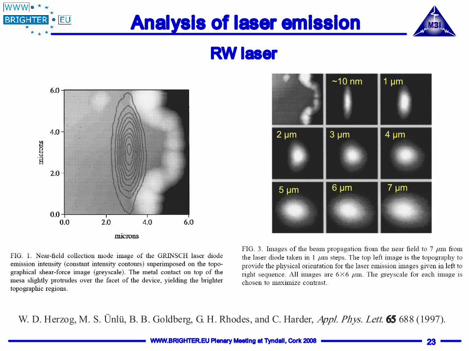
Analysis of laser emission
W. D. Herzog, M. S. Ünlü, B. B. Goldberg, G. H. Rhodes, and C. Harder, (1997). Appl. Phys. Lett. 65 688
RW laser ~10 nm 1 µm
2 µm 3 µm 4 µm
5 µm 6 µm 7 µm
23 WWW.BRIGHTER.EU Plenary Meeting at Tyndall, Cork 2008

Analysis of laser emission VCSEL
I=7 mA I=10 mA I=15 mA
VCSEL aperture (blue)
Emission intensity (color)
Van der Rhodes et al. Appl. Phys. Lett. 72,1811 (1998)
24 WWW.BRIGHTER.EU Plenary Meeting at Tyndall, Cork 2008

Analysis of laser emission
Such work at devices is extremely useful,
1. if confocal microscopy fails
2. if the fiber tip does not influence the emission
These statements hold in general for the application of NSOM !
if not, you waste your resources
unfortunately, this is the case when investigating lasing devices
25 WWW.BRIGHTER.EU Plenary Meeting at Tyndall, Cork 2008

What is better?
Spontaneous emission Photoluminescence Absorption (Photocurrent)
fiber tip
heat sink
Substrate ARcoating
cladding
waveguide DQW
heat sink
cladding lockin amplifier
26 WWW.BRIGHTER.EU Plenary Meeting at Tyndall, Cork 2008

What is better?
Spontaneous emission Photoluminescence Absorption (Photocurrent)
fiber tip
heat sink
Substrate ARcoating
cladding
waveguide DQW
heat sink
cladding lockin amplifier
27 WWW.BRIGHTER.EU Plenary Meeting at Tyndall, Cork 2008

What is better?
Spontaneous emission Photoluminescence Absorption (Photocurrent) NOBIC
fiber tip
heat sink
Substrate ARcoating
cladding
waveguide DQW
heat sink
cladding lockin amplifier
28 WWW.BRIGHTER.EU Plenary Meeting at Tyndall, Cork 2008

NOBIC
NOBIC signal (a.u.)
NOBIC = Nearfield Optical Beam Induced Current
Buratto et al. (AT&T Bell Lab.) Appl. Phys. Lett. 65, 2654 (1994)
Excitation at 633 nm (2 mW in, ~2 nW out)
NOBIC
A
B
29 WWW.BRIGHTER.EU Plenary Meeting at Tyndall, Cork 2008

Outline
1. Introduction NSOM = Nearfield Scanning Optical Microscopy Principles and opportunities Spatial resolution
2. Methodology Laser emission, spontaneous emission and PL
3. NOBIC = Nearfield Optical Beam Induced Current 4. Experimental setups and equipment 5. Analysis of waveguides and determination of mode profiles 6. VCSEL 7. Surface recombination velocity at facets 8. Defect creation during device operation 9. Summary 10. Acknowledgement
30 WWW.BRIGHTER.EU Plenary Meeting at Tyndall, Cork 2008

Experimental setups and equipment
31 WWW.BRIGHTER.EU Plenary Meeting at Tyndall, Cork 2008

Fibertip distance control
Experimental setups and equipment
32 WWW.BRIGHTER.EU Plenary Meeting at Tyndall, Cork 2008

Experimental setups and equipment
Fibertip distance control
33 WWW.BRIGHTER.EU Plenary Meeting at Tyndall, Cork 2008
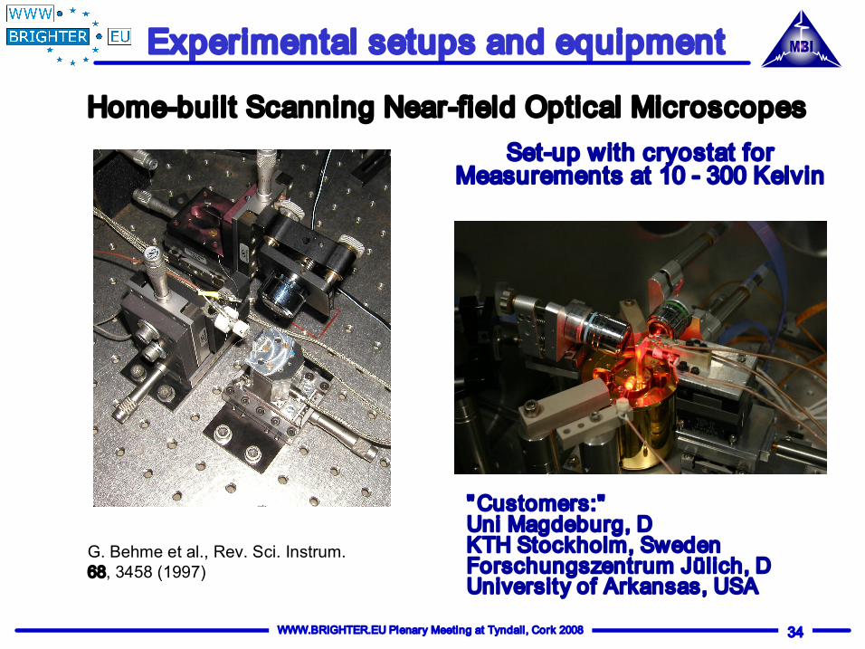
Homebuilt Scanning Nearfield Optical Microscopes Setup with cryostat for
Measurements at 10 300 Kelvin
"Customers:" Uni Magdeburg, D KTH Stockholm, Sweden Forschungszentrum Jülich, D University of Arkansas, USA
G. Behme et al., Rev. Sci. Instrum. 68, 3458 (1997)
Experimental setups and equipment
34 WWW.BRIGHTER.EU Plenary Meeting at Tyndall, Cork 2008

NSOM data
PCsignal (R) topography
Experimental setups and equipment
35 WWW.BRIGHTER.EU Plenary Meeting at Tyndall, Cork 2008

Outline
1. Introduction NSOM = Nearfield Scanning Optical Microscopy Principles and opportunities Spatial resolution
2. Methodology Laser emission, spontaneous emission and PL
3. NOBIC = Nearfield Optical Beam Induced Current 4. Experimental setups and equipment 5. Analysis of waveguides and determination of mode profiles 6. VCSEL 7. Surface recombination velocity at facets 8. Defect creation during device operation 9. Summary 10. Acknowledgement
36 WWW.BRIGHTER.EU Plenary Meeting at Tyndall, Cork 2008

Analysis of waveguides
Heat sink Substrate
LOC waveguide Cladding layer
Double quantum well
AR coating AR coating AR coating
Modulator (1.2 kHz)
AR coating
Excitation laser Lockin amplifier
Lockin amplifier
PC
Setup
37 WWW.BRIGHTER.EU Plenary Meeting at Tyndall, Cork 2008

Results obtained at single symmetric and asymmetric waveguides
resonant NSOM Photocurrent (Absorption)
Step INdex SIN
Large Optical Cavity LOC symmetric waveguide
Large Optical Cavity LOC asymmetric waveguide
0 1 2 3 4 5
potential
x (µm)
0 1 2 3 4 5
potential
x (µm)
0 1 2 3 4 5
potential
x (µm)
Analysis of waveguides
38 WWW.BRIGHTER.EU Plenary Meeting at Tyndall, Cork 2008

1 0 1 0.0
0.5
1.0
1.5
2.0
PC Signal (a.u.)
Tip Position (µm) 1 0 1 0.0
0.2
0.4
0.6
0.8
1.0
1.2
PC Signal (a.u.)
Tip Position (µm) 1 0 1 0.0
0.2
0.4
0.6
0.8
1.0
1.2
PC Signal (a.u.)
Tip Position (µm)
Step INdex SIN
Large Optical Cavity LOC symmetric waveguide
Large Optical Cavity LOC asymmetric waveguide
1 0 1
m=2
m=1
m=0
Position (µm) 1 0 1
m=2
m=1
m=0
Position (µm)
1 0 1
Position (µm)
Analysis of waveguides
39 WWW.BRIGHTER.EU Plenary Meeting at Tyndall, Cork 2008

Comparison of the guided modes in a waveguide and the wavefunctions in a quantum well
Analysis of waveguides
40 WWW.BRIGHTER.EU Plenary Meeting at Tyndall, Cork 2008

Step INdex SIN
Large Optical Cavity LOC symmetric waveguide
Large Optical Cavity LOC asymmetric waveguide
1 0 1 0.0
0.5
1.0
1.5
2.0
2.5
PC Signal (a.u.)
Tip Position (µm) 1 0 1 0.0
0.5
1.0
PC Signal (a.u.)
Tip Position (µm) 1 0 1 0.0
0.2
0.4
0.6
0.8
1.0
1.2
PC Signal (a.u.)
Tip Position (µm)
NSOM Photocurrent reveals mode structure of waveguides asymmetric waveguides have a specific NSOM Photocurrent signature
Analysis of waveguides
41 WWW.BRIGHTER.EU Plenary Meeting at Tyndall, Cork 2008

2 1 0 1 2 0,0
0,5
1,0
1,5
2,0
2,5
excitation photon energy: 2.8 eV
absolute value phase
NOBIC line scans from the symmetric LOC structure
Absolute Value,Φ, and E g
(a.u., °, and eV)
x (µm) 2 1 0 1 2
0,0
1,0
2,0
3,0
NOBIC line scans from the asymmetric LOC structure
(117+24) nm excitation photon energy: 2.8 eV
absolute value phase
Absolute value,
Φ, and E g
(a.u., °, and eV)
x (µm)
NOBIC contrast from the photocurrent phase for non resonant (surface) excitation
Analysis of waveguides
42 WWW.BRIGHTER.EU Plenary Meeting at Tyndall, Cork 2008

Single waveguides Resonant excitation (coupling into the
waveguide modes) NOBIC reveals mode structure of waveguides asymmetric waveguides have a specific NOBIC
signature Nonresonant excitation (pure carrierpair creation) detection of the QW within the waveguide
T. Guenther et al. „NearField Photocurrent Imaging of the Optical Mode Profiles of Semiconductor Laser Diodes“ Appl. Phys. Lett. 78 14631465 (2001).
Analysis of waveguides
43 WWW.BRIGHTER.EU Plenary Meeting at Tyndall, Cork 2008
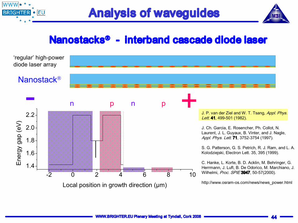
2 0 2 4 6 8 10 1.4
1.6
1.8
2.0
2.2
Energy gap (e
V)
Local position in growth direction (µm)
Nanostacks interband cascade diode laser
n n p p + J. P. van der Ziel and W. T. Tsang, Appl. Phys. Lett. 41, 499501 (1982).
J. Ch. Garcia, E. Rosencher, Ph. Collot, N. Laurent, J. L. Guyaux, B. Vinter, and J. Nagle, Appl. Phys. Lett. 71, 37523754 (1997).
S. G. Patterson, G. S. Petrich, R. J. Ram, and L. A. Kolodziejski, Electron Lett. 35, 395 (1999).
C. Hanke, L. Korte, B. D. Acklin, M. Behringer, G. Herrmann, J. Luft, B. De Odorico, M. Marchiano, J. Wilhelmi, Proc. SPIE 3947, 5057(2000).
http://www.osramos.com/news/news_power.html
‘regular’ highpower diode laser array
Nanostack
Analysis of waveguides
44 WWW.BRIGHTER.EU Plenary Meeting at Tyndall, Cork 2008

1 2 3 4 5 6 7 8
1
2
3
4
5
6
7
8
y (µm)
x (µm)
Photoluminescence Photocurrent (Absorption) Device emission
Detailed analysis of Nano stacks by NSOMbased
spectroscopy
Analysis of waveguides
45 WWW.BRIGHTER.EU Plenary Meeting at Tyndall, Cork 2008

Results from Nanostacks with two vertically stacked asymmetric waveguides
0 2 4 6 8 10 0.0
0.2
0.4
0.6
0.8
1.0
x (µm)
Electroluminescence (a. u.)
0 2 4 6 8 10 0.0
0.2
0.4
0.6
0.8
1.0
x (µm)
Laser signal (a.u.)
NSOM Device Emission
Substrate duty cycle: 2x10 5 no thermal load
Analysis of waveguides
46 WWW.BRIGHTER.EU Plenary Meeting at Tyndall, Cork 2008

NSOM PL Emission
0 2 4 6 8 10 0.00
0.25
0.50
0.75
1.00
x (µm)
PL signal (a
. u.)
0 2 4 6 8 10 0.0
0.2
0.4
0.6
0.8
1.0
11 µW 160 nW 16 nW
x (µm)
PL signal (a
. u.)
excitation photon energy: 2.8 eV detection photon energy: 1.5 eV
excitation photon energy: 1.69 eV detection photon energy: 1.5 eV
PLsignal ~ δn
Analysis of waveguides
47 WWW.BRIGHTER.EU Plenary Meeting at Tyndall, Cork 2008

resonant and nonresonant NSOM Photocurrent (Absorption)
0 2 4 6 8 10 0.0
0.2
0.4
0.6
0.8
1.0
x (µm) PC Signal (a. u.)
0 2 4 6 8 10 0.0
0.2
0.4
0.6
0.8
1.0
x (µm)
PC signal (a. u.)
excitation photon energy: 1.69 eV excitation photon energy: 2.8 eV
Photocurrentsignal ~ δn×grad(V)
Analysis of waveguides
V. Malyarchuk et al. "Uniformity tests of individual segments of interband cascade diode laser nanostacks " J. Appl. Phys. 92, 27292733 (2002).
48 WWW.BRIGHTER.EU Plenary Meeting at Tyndall, Cork 2008

0.4 0.6 0.8 1.0 1.2 1.4 1.6 1.8 10 5 10 4 10 3 10 2 10 1 10 0
onset of the Braggmirror absorption at about 1.62 eV
'barrier absorption' due to the Al 0.25 Ga 0.75 As barriers
'QW region' 'defect region'
VCSEL emission energy
Photocurre
nt (a.u.)
Photon energy (eV)
NOBIC at VCSELS
49 WWW.BRIGHTER.EU Plenary Meeting at Tyndall, Cork 2008

Outline
1. Introduction NSOM = Nearfield Scanning Optical Microscopy Principles and opportunities Spatial resolution
2. Methodology Laser emission, spontaneous emission and PL
3. NOBIC = Nearfield Optical Beam Induced Current 4. Experimental setups and equipment 5. Analysis of waveguides and determination of mode profiles 6. VCSEL 7. Surface recombination velocity at facets 8. Defect creation during device operation 9. Summary 10. Acknowledgement
50 WWW.BRIGHTER.EU Plenary Meeting at Tyndall, Cork 2008

Reflection PL experiment uncoated fiber tip spatial resolution: 150 nm
Surface Recombination Velocity
v s
V. Malyarchuk, J. W. Tomm, V. Talalaev, Ch. Lienau, F. Rinner, and M. Baeumler Appl. Phys. Lett. 81 346 (2002).
L D
51 WWW.BRIGHTER.EU Plenary Meeting at Tyndall, Cork 2008

1 0 1 2 3 0
1
2
PL
x (µm)
y (µm)
0 0.5 1.0
1 0 1 2 3 0
1
2
PL
x (µm)
y (µm)
0 0.5 1.0
1 0 1 2 3 0
1
2
∆PL
x (µm)
y (µm)
0.06 0 0.06
1 0 1 2 3 0
1
2
∆PL
x (µm)
y (µm)
0.06 0 0.06
P = 10 µW P = 300 µW
QW PL collected through the fiber and detected by a single photon counting system
Lineleveled images
Surface Recombination Velocity
52 WWW.BRIGHTER.EU Plenary Meeting at Tyndall, Cork 2008

0.0 1.0 2.0 0.0
0.5
1.0
300 µW 100 µW 30 µW R
Signal (a.u.)
x (µm)
Surface Recombination Velocity
53 WWW.BRIGHTER.EU Plenary Meeting at Tyndall, Cork 2008

0.0 1.0 2.0 0.0
0.5
1.0
PL v s = 0.5 x 10 6 cm/s
v s = 1.0 x 10 6 cm/s
v s = 3.0 x 10 6 cm/s
PL (a.u.)
x (µm)
D = 15 cm 2 /s τ = 1.7 ns
D rec L D τ =
2 2
0 0 2 2 ( ) ( , ) 0 a rec
n D n n g x y x y
∂ ∂ ∂ ∂ τ
+ − + =
2 2 0 0
2 ( ) ( )
2 0 0
1 ( , ) 2
x x y y
g x y e σ
πσ
− + − −
=
x=0: 0
v s x
n D n x
∂ ∂ =
= ⋅
diffusion length L D and the product (v ) s rec τ ⋅ can be deduced
Surface Recombination Velocity
Example calculated for:
54 WWW.BRIGHTER.EU Plenary Meeting at Tyndall, Cork 2008

0.0 1.0 2.0 0.0
0.5
1.0
300 µW 100 µW 30 µW R
Signal (a.u.)
x (µm)
L D
v s *☺
Surface Recombination Velocity
55 WWW.BRIGHTER.EU Plenary Meeting at Tyndall, Cork 2008

0.0
0.5
1.0
1.5
2.0
2.5
1 10 100 1000 0.5
1.0
1.5
2.0
2.5
3.0 L D
(µm)
Power (µW)
τ QW (n
s)
Additional ps PLexperiment provides τ
Surface Recombination Velocity
56 WWW.BRIGHTER.EU Plenary Meeting at Tyndall, Cork 2008

0
10
20
30
1 10 100 1000 0.0
2.0
4.0
6.0
8.0 v s
(10 6
cm/s)
Power (µW)
D (cm 2 /s)
Surface Recombination Velocity
V. Malyarchuk, J. W. Tomm, V. Talalaev, Ch. Lienau, F. Rinner, and M.Baeumler Appl. Phys. Lett. 81 346 (2002).
57 WWW.BRIGHTER.EU Plenary Meeting at Tyndall, Cork 2008
Outline
1. Introduction NSOM = Nearfield Scanning Optical Microscopy Principles and opportunities Spatial resolution
2. Methodology Laser emission, spontaneous emission and PL
3. NOBIC = Nearfield Optical Beam Induced Current 4. Experimental setups and equipment 5. Analysis of waveguides and determination of mode profiles 6. VCSEL 7. Surface recombination velocity at facets 8. Defect creation during device operation 9. Summary 10. Acknowledgement
58 WWW.BRIGHTER.EU Plenary Meeting at Tyndall, Cork 2008
1.0 1.5 2.0 2.5 3.0
10 2
10 1
10 0
10 1
10 2
10 3
10 4 PC FTIR Spectra Red LD OSRAM 510311
PC signal (a.u.)
Energy (eV)
Before Aging 9h Aging 30h Aging 55h Aging
0.0 0.2 0.4 0.6 0.8 0
20
40
60
80
100
120
140
160
180
200
0.0
0.5
1.0
1.5
2.0
2.5 Osram (BRIGHT) 51011+3
Pow
er (m
W)
Current (A)
0h 0.5h 1.5h 3h 9h 15h 31h 55h
Voltage (V
)
Defect creation during device operation
Result from the BRIGHT project
59 WWW.BRIGHTER.EU Plenary Meeting at Tyndall, Cork 2008

1.0 1.2 1.4 1.6 1.8
10 2
10 1
10 0
PC FTIR Spectra Red LD OSRAM 510311
PC signal (a.u.)
Energy (eV)
Before Aging 9h Aging 30h Aging 55h Aging
DefecttoBand Transitions?
Where are the ‘defects’ located?
Active region???
At 1.7 eV (730 nm), there is a threefold increase of the signal within 55 h of aging.
Defect creation during device operation
60 WWW.BRIGHTER.EU Plenary Meeting at Tyndall, Cork 2008

1. Laterally, i.e., where along the device…
0.0 0.2 0.4 0.6 0.00
0.05
0.10
0.15
0.20
Osram (BRIGHT) 51011+3
pristine device 3h 9h
LBIC signal (a.u.)
y (mm) LBIC (Laser Beam Induced Current) excited resonantly to the defects reveals them to be underneath the metalized emitter stripe.
Front view of the laser structure
substrate
epilayer sequence
active region
Defect creation during device operation
61 WWW.BRIGHTER.EU Plenary Meeting at Tyndall, Cork 2008

2. Vertically, i.e., where along the layer sequence …
aged area
‘Pristine’ reference area
Front view of the laser structure substrate
~ 1.5 µm
Defect creation during device operation
62 WWW.BRIGHTER.EU Plenary Meeting at Tyndall, Cork 2008

633 nm 730 nm topography
pristine device region
1000 nm 1000 nm 1000 nm
NOBICData: (Nearfield Optical Beam Induced Current)
Defect creation during device operation
63 WWW.BRIGHTER.EU Plenary Meeting at Tyndall, Cork 2008

0.0 0.5 1.0 1.5 2.0 10 2
10 1
10 0
10 1 633 nm 730 nm
aged region Signal (a
.u.)
x (µm)
633 nm 730 nm topography
aged device region
1000 nm 1000 nm 1000 nm
Defect creation during device operation
64 WWW.BRIGHTER.EU Plenary Meeting at Tyndall, Cork 2008

0.0 0.5 1.0 1.5 2.0
10 2
10 1
10 0
10 1
633 nm 730 nm
Signal (a.u.)
x (µm)
pristine region
0.0 0.5 1.0 1.5 2.0
10 2
10 1
10 0
10 1
633 nm 730 nm
aged region
Signal (a.u.)
x (µm) 1.5 µm 1.5 µm
There is a threefold increase of the 730 nm signal with respect to the 633 nmsignal 1.5 µm away from the active region (towards the heat sink), there is no photosensitivity.
The creation of deep levels takes place at a location that allows interaction with the laser emission.
There are additional 3 sets of data couples from different regions, which confirm the result.
Defect creation during device operation
Claus Ropers et al. Appl. Phys. Lett. 88, 133513 (2006).
65 WWW.BRIGHTER.EU Plenary Meeting at Tyndall, Cork 2008

NSOM = Nearfield Scanning Optical Microscopy Principles and opportunities Spatial resolution
Methodology, Laser emission, spontaneous emission and PL NOBIC = Nearfield Optical Beam Induced Current Experimental setups and equipment Analysis of waveguides and determination of mode profiles VCSEL Surface recombination velocity at facets Defect creation during device operation
Summary
NSOM is extremely useful if you need a spatial resolution beyond the diffraction limit.
NOBIC allows optical analysis at devices along growth direction.
66 WWW.BRIGHTER.EU Plenary Meeting at Tyndall, Cork 2008

• Christoph Lienau
• Alexander Richter, Tobias Günther, Viktor Malyarchuk, Roland Müller, Claus Ropers, Thomas Elsässer
• Martin Behringer, Johannes Luft, Peter Brick, Norbert Linder, Bernd Mayer, Martin Müller, Sönke Tautz, Wolfgang Schmid, Götz Erbert, Jürgen Sebastian, Siegfried Gramlich, Eberhard Richter, Heiko Kissel, Frank Brunner, Markus Weyers, Günter Tränkle
Acknowledgement
67 WWW.BRIGHTER.EU Plenary Meeting at Tyndall, Cork 2008