- Small LES COB line-up - C-Series Gen - Cloud Object ... · - Small LES COB line-up - C-Series...
21
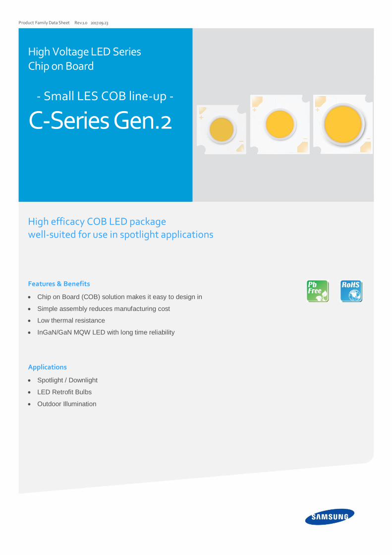
1# Product Family Data Sheet Rev.1.0 2017.09.23 High Voltage LED Series Chip on Board - Small LES COB line-up - C-Series Gen.2 High efficacy COB LED package well-suited for use in spotlight applications Features & Benefits Chip on Board (COB) solution makes it easy to design in Simple assembly reduces manufacturing cost Low thermal resistance InGaN/GaN MQW LED with long time reliability Applications Spotlight / Downlight LED Retrofit Bulbs Outdoor Illumination
Transcript of - Small LES COB line-up - C-Series Gen - Cloud Object ... · - Small LES COB line-up - C-Series...
1#
Product Family Data Sheet Rev.1.0 2017.09.23
High Voltage LED Series Chip on Board
- Small LES COB line-up -
C-Series Gen.2
High efficacy COB LED package well-suited for use in spotlight applications
Features & Benefits
Chip on Board (COB) solution makes it easy to design in
Simple assembly reduces manufacturing cost
Low thermal resistance
InGaN/GaN MQW LED with long time reliability
Applications
Spotlight / Downlight
LED Retrofit Bulbs
Outdoor Illumination
2
Table of Contents
1. Characteristics ----------------------- 3
2. Product Code Information ----------------------- 6
3. Typical Characteristics Graphs ----------------------- 10
4. Outline Drawing & Dimension ----------------------- 13
5. Label Structure ----------------------- 17
6. Packing Structure ----------------------- 18
7. Precautions in Handling & Use ----------------------- 20
3
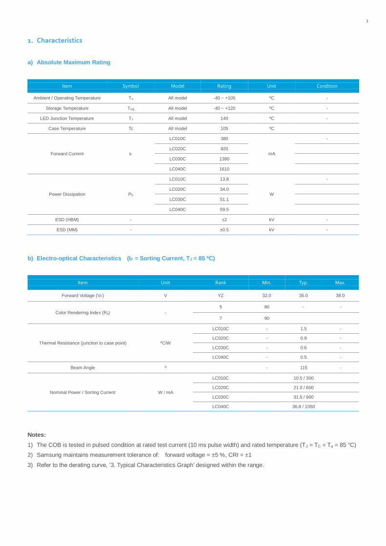
1. Characteristics
a) Absolute Maximum Rating
Item Symbol Model Rating Unit Condition
Ambient / Operating Temperature Ta All model -40 ~ +105 ºC -
Storage Temperature Tstg All model -40 ~ +120 ºC -
LED Junction Temperature TJ All model 140 ºC -
Case Temperature Tc All model 105 ºC
Forward Current IF
LC010C 380
mA
-
LC020C 920
LC030C 1380
LC040C 1610
Power Dissipation PD
LC010C 13.8
W
-
LC020C 34.0
LC030C 51.1
LC040C 59.5
ESD (HBM) - ±2 kV -
ESD (MM) - ±0.5 kV -
b) Electro-optical Characteristics (IF = Sorting Current, TJ = 85 ºC)
Item Unit Rank Min. Typ. Max.
Forward Voltage (VF) V YZ 32.0 35.0 38.0
Color Rendering Index (Ra) -
5 80 - -
7 90
Thermal Resistance (junction to case point) ºC/W
LC010C - 1.5 -
LC020C - 0.9 -
LC030C - 0.6 -
LC040C - 0.5 -
Beam Angle º - 115 -
Nominal Power / Sorting Current W / mA
LC010C 10.5 / 300
LC020C 21.0 / 600
LC030C 31.5 / 900
LC040C 36.8 / 1050
Notes:
1) The COB is tested in pulsed condition at rated test current (10 ms pulse width) and rated temperature (TJ = TC = Ta = 85 °C)
2) Samsung maintains measurement tolerance of: forward voltage = ±5 %, CRI = ±1
3) Refer to the derating curve, ‘3. Typical Characteristics Graph’ designed within the range.
4
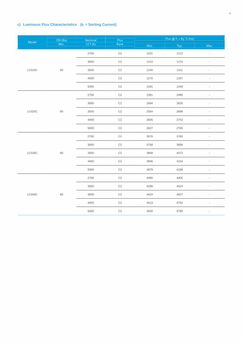
c) Luminous Flux Characteristics (IF = Sorting Current)
Model CRI (Ra)
Min. Nominal CCT (K)
Flux Rank
Flux @ TJ = 85 °C (lm)
Min. Typ. Max.
LC010C 80
2700 C2 1151 1212 -
3000 C2 1210 1274 -
3500 C2 1245 1311 -
4000 C2 1270 1337 -
5000 C2 1281 1348 -
LC020C 80
2700 C2 2361 2485 -
3000 C2 2494 2625 -
3500 C2 2554 2688 -
4000 C2 2605 2742 -
5000 C2 2627 2765 -
LC030C 80
2700 C2 3576 3765 -
3000 C2 3758 3956 -
3500 C2 3868 4072 -
4000 C2 3946 4154 -
5000 C2 3979 4188 -
LC040C 80
2700 C2 4090 4305 -
3000 C2 4298 4524 -
3500 C2 4424 4657 -
4000 C2 4513 4750 -
5000 C2 4550 4790 -
5
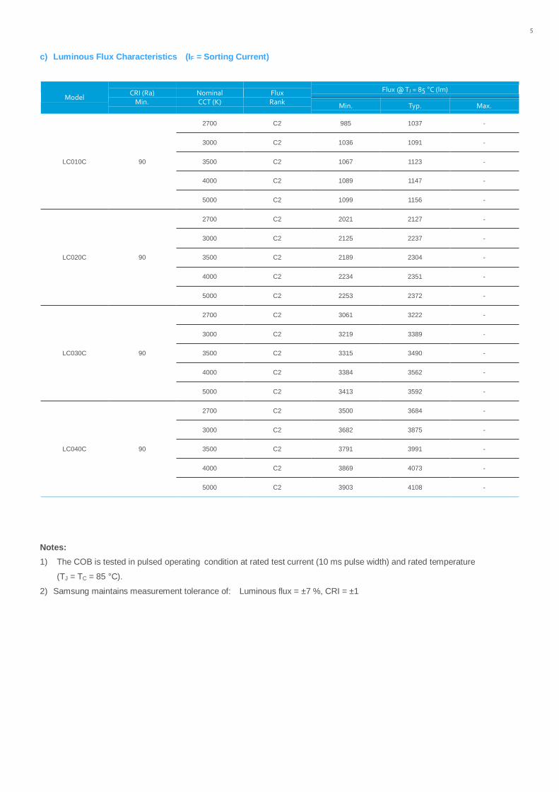
c) Luminous Flux Characteristics (IF = Sorting Current)
Model CRI (Ra)
Min. Nominal CCT (K)
Flux Rank
Flux @ TJ = 85 °C (lm)
Min. Typ. Max.
LC010C 90
2700 C2 985 1037 -
3000 C2 1036 1091 -
3500 C2 1067 1123 -
4000 C2 1089 1147 -
5000 C2 1099 1156 -
LC020C 90
2700 C2 2021 2127 -
3000 C2 2125 2237 -
3500 C2 2189 2304 -
4000 C2 2234 2351 -
5000 C2 2253 2372 -
LC030C 90
2700 C2 3061 3222 -
3000 C2 3219 3389 -
3500 C2 3315 3490 -
4000 C2 3384 3562 -
5000 C2 3413 3592 -
LC040C 90
2700 C2 3500 3684 -
3000 C2 3682 3875 -
3500 C2 3791 3991 -
4000 C2 3869 4073 -
5000 C2 3903 4108 -
Notes:
1) The COB is tested in pulsed operating condition at rated test current (10 ms pulse width) and rated temperature
(TJ = TC = 85 °C).
2) Samsung maintains measurement tolerance of: Luminous flux = ±7 %, CRI = ±1
6
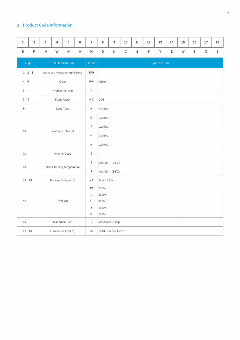
2. Product Code Information
1 2 3 4 5 6 7 8 9 10 11 12 13 14 15 16 17 18
S P H W H A H D N C 2 5 Y Z W 3 C 2
Digit PKG Information Code Specification
1 2 3 Samsung Package High Power SPH
4 5 Color WH White
6 Product Version A
7 8 Form Factor HD COB
9 Lens Type N No lens
10 Wattage or Model
C LC010C
F LC020C
H LC030C
K LC040C
11 Internal Code 2
12 CRI & Sorting Temperature
5 Min. 80 (85℃)
7 Min. 90 (85℃)
13 14 Forward Voltage (V) YZ 32.0 ~ 38.0
15 CCT (K)
W 2700K
V 3000K
U 3500K
T 4000K
R 5000K
16 MacAdam Step 3 MacAdam 3-step
17 18 Luminous Flux (Lm) C2 COB C-series Gen2

7
a) Binning Structure (IF = Sorting Current, TJ = 85 ºC)
Model CRI (Ra)
Min. Nominal CCT (K)
Product Code VF
Rank Color Rank
Flux Rank
Flux Range (Φv, lm)
LC010C 80
2700 SPHWHAHDNC25YZW3C2 YZ W3 C2 1151 ~
3000 SPHWHAHDNC25YZV3C2 YZ V3 C2 1210 ~
3500 SPHWHAHDNC25YZU3C2 YZ U3 C2 1245 ~
4000 SPHWHAHDNC25YZT3C2 YZ T3 C2 1270 ~
5000 SPHWHAHDNC25YZR3C2 YZ R3 C2 1281 ~
LC020C 80
2700 SPHWHAHDNF25YZW3C2 YZ W3 C2 2361 ~
3000 SPHWHAHDNF25YZV3C2 YZ V3 C2 2494 ~
3500 SPHWHAHDNF25YZU3C2 YZ U3 C2 2554 ~
4000 SPHWHAHDNF25YZT3C2 YZ T3 C2 2605 ~
5000 SPHWHAHDNF25YZR3C2 YZ R3 C2 2627 ~
LC030C 80
2700 SPHWHAHDNH25YZW3C2 YZ W3 C2 3576 ~
3000 SPHWHAHDNH25YZV3C2 YZ V3 C2 3758 ~
3500 SPHWHAHDNH25YZU3C2 YZ U3 C2 3868 ~
4000 SPHWHAHDNH25YZT3C2 YZ T3 C2 3946 ~
5000 SPHWHAHDNH25YZR3C2 YZ R3 C2 3979 ~
LC040C 80
2700 SPHWHAHDNK25YZW3C2 YZ W3 C2 4090 ~
3000 SPHWHAHDNK25YZV3C2 YZ V3 C2 4298 ~
3500 SPHWHAHDNK25YZU3C2 YZ U3 C2 4424 ~
4000 SPHWHAHDNK25YZT3C2 YZ T3 C2 4513 ~
5000 SPHWHAHDNK25YZR3C2 YZ R3 C2 4550 ~
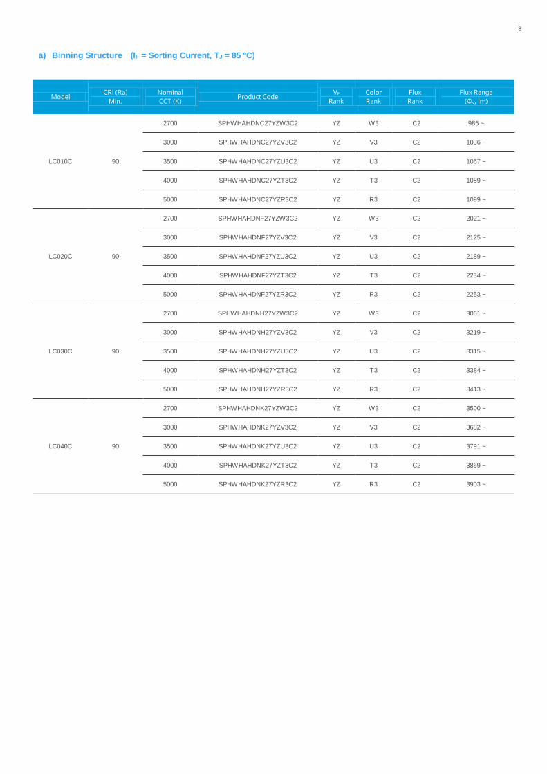
8
a) Binning Structure (IF = Sorting Current, TJ = 85 ºC)
Model CRI (Ra)
Min. Nominal CCT (K)
Product Code VF
Rank Color Rank
Flux Rank
Flux Range (Φv, lm)
LC010C 90
2700 SPHWHAHDNC27YZW3C2 YZ W3 C2 985 ~
3000 SPHWHAHDNC27YZV3C2 YZ V3 C2 1036 ~
3500 SPHWHAHDNC27YZU3C2 YZ U3 C2 1067 ~
4000 SPHWHAHDNC27YZT3C2 YZ T3 C2 1089 ~
5000 SPHWHAHDNC27YZR3C2 YZ R3 C2 1099 ~
LC020C 90
2700 SPHWHAHDNF27YZW3C2 YZ W3 C2 2021 ~
3000 SPHWHAHDNF27YZV3C2 YZ V3 C2 2125 ~
3500 SPHWHAHDNF27YZU3C2 YZ U3 C2 2189 ~
4000 SPHWHAHDNF27YZT3C2 YZ T3 C2 2234 ~
5000 SPHWHAHDNF27YZR3C2 YZ R3 C2 2253 ~
LC030C 90
2700 SPHWHAHDNH27YZW3C2 YZ W3 C2 3061 ~
3000 SPHWHAHDNH27YZV3C2 YZ V3 C2 3219 ~
3500 SPHWHAHDNH27YZU3C2 YZ U3 C2 3315 ~
4000 SPHWHAHDNH27YZT3C2 YZ T3 C2 3384 ~
5000 SPHWHAHDNH27YZR3C2 YZ R3 C2 3413 ~
LC040C 90
2700 SPHWHAHDNK27YZW3C2 YZ W3 C2 3500 ~
3000 SPHWHAHDNK27YZV3C2 YZ V3 C2 3682 ~
3500 SPHWHAHDNK27YZU3C2 YZ U3 C2 3791 ~
4000 SPHWHAHDNK27YZT3C2 YZ T3 C2 3869 ~
5000 SPHWHAHDNK27YZR3C2 YZ R3 C2 3903 ~
9
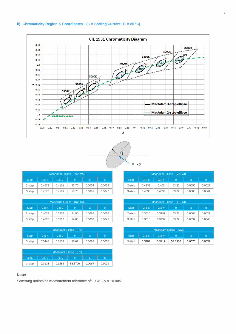
b) Chromaticity Region & Coordinates (IF = Sorting Current, TJ = 85 ºC)
MacAdam Ellipse (W2, W3) MacAdam Ellipse (V2, V3)
Step CIE x CIE y a b Step CIE x CIE y a b
2-step 0.4578 0.4101 53.70 0.0054 0.0028 2-step 0.4338 0.403 53.22 0.0056 0.0027
3-step 0.4578 0.4101 53.70 0.0081 0.0042 3-step 0.4338 0.4030 53.22 0.0083 0.0041
MacAdam Ellipse (U2, U3) MacAdam Ellipse (T2, T3)
Step CIE x CIE y a b Step CIE x CIE y a b
2-step 0.4073 0.3917 54.00 0.0062 0.0028 2-step 0.3818 0.3797 53.72 0.0063 0.0027
3-step 0.4073 0.3917 54.00 0.0093 0.0041 3-step 0.3818 0.3797 53.72 0.0094 0.0040
MacAdam Ellipse (R3) MacAdam Ellipse (Q3)
Step CIE x CIE y a b Step CIE x CIE y a b
3-step 0.3447 0.3553 59.62 0.0082 0.0035 3-step 0.3287 0.3417 59.0950 0.0075 0.0032
MacAdam Ellipse (P3)
Step CIE x CIE y a b
3-step 0.3123 0.3282 58.5700 0.0067 0.0029
Note:
Samsung maintains measurement tolerance of: Cx, Cy = ±0.005
CIE x,y
10
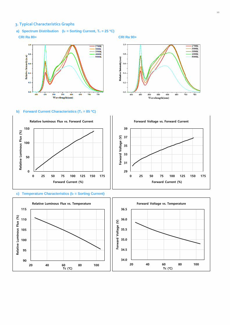
3. Typical Characteristics Graphs
a) Spectrum Distribution (IF = Sorting Current, Tc = 25 ºC)
CRI Ra 80+ CRI Ra 90+
b) Forward Current Characteristics (Tc = 85 ºC)
c) Temperature Characteristics (IF = Sorting Current)
0
50
100
150
0 25 50 75 100 125 150 175
Rela
tive L
um
inous
Flu
x (
%)
Forward Current (%)
Relative luminous Flux vs. Forward Current
29
31
33
35
37
39
0 25 50 75 100 125 150 175
Forw
ard
Voltage (
V)
Forward Current (%)
Forward Voltage vs. Forward Current
90
95
100
105
110
115
20 40 60 80 100
Rela
tive L
um
inous
Flu
x (
%)
Tc (℃)
Relative Luminous Flux vs. Temperature
34.0
34.5
35.0
35.5
36.0
36.5
20 40 60 80 100
Forw
ard
Voltage (
V)
Tc (℃)
Forward Voltage vs. Temperature
11
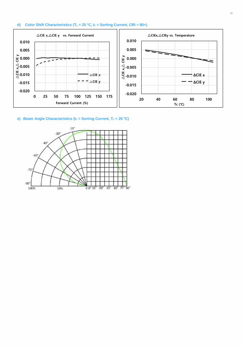
d) Color Shift Characteristics (Tc = 25 ºC, IF = Sorting Current, CRI = 80+)
e) Beam Angle Characteristics (IF = Sorting Current, Tc = 25 ºC)
-0.020
-0.015
-0.010
-0.005
0.000
0.005
0.010
0 25 50 75 100 125 150 175
△CIE
x,△
CIE
y
Forward Current (%)
△CIE x,△CIE y vs. Forward Current
△CIE x
△CIE y
-0.020
-0.015
-0.010
-0.005
0.000
0.005
0.010
20 40 60 80 100
△CIE
x,△
CIE
y
Tc (℃)
△CIEx,△CIEy vs. Temperature
ΔCIE x
ΔCIE y
12
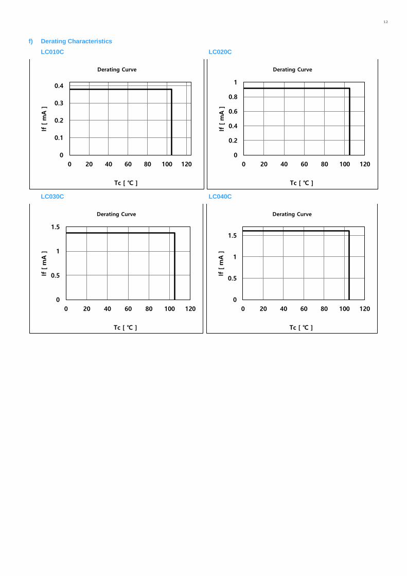
f) Derating Characteristics
LC010C LC020C
LC030C LC040C
0
0.1
0.2
0.3
0.4
0 20 40 60 80 100 120
If [
mA
]
Tc [ ℃ ]
Derating Curve
0
0.2
0.4
0.6
0.8
1
0 20 40 60 80 100 120
If [
mA
]
Tc [ ℃ ]
Derating Curve
0
0.5
1
1.5
0 20 40 60 80 100 120
If [
mA
]
Tc [ ℃ ]
Derating Curve
0
0.5
1
1.5
0 20 40 60 80 100 120
If [
mA
]
Tc [ ℃ ]
Derating Curve
13
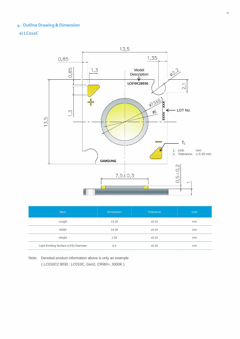
4. Outline Drawing & Dimension
a) LC010C
Item Dimension Tolerance Unit
Length 13.35 ±0.15 mm
Width 13.35 ±0.15 mm
Height 1.50 ±0.20 mm
Light Emitting Surface (LES) Diameter 6.0 ±0.30 mm
Note: Denoted product information above is only an example
( LC010C2 8030 : LC010C, Gen2, CRI80+, 3000K )
1. Unit: mm 2. Tolerance: ± 0.30 mm
LC010C28030
Model Description
XXX.....X
XXX
LOT No.
SAMSUNG
TC
14
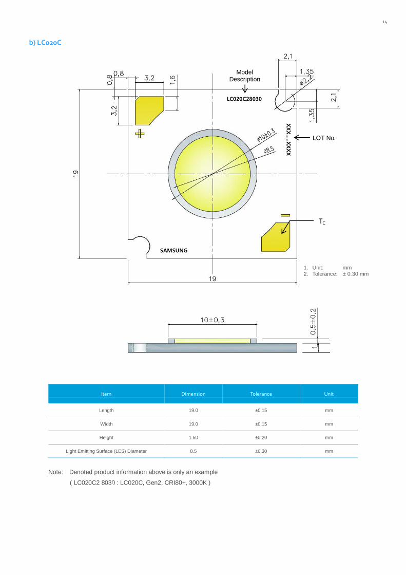
b) LC020C
Item Dimension Tolerance Unit
Length 19.0 ±0.15 mm
Width 19.0 ±0.15 mm
Height 1.50 ±0.20 mm
Light Emitting Surface (LES) Diameter 8.5 ±0.30 mm
Note: Denoted product information above is only an example
( LC020C2 8030 : LC020C, Gen2, CRI80+, 3000K )
1. Unit: mm 2. Tolerance: ± 0.30 mm
Model Description
LOT No.
SAMSUNG
LC020C28030
XXX.....X
XXX
TC
15
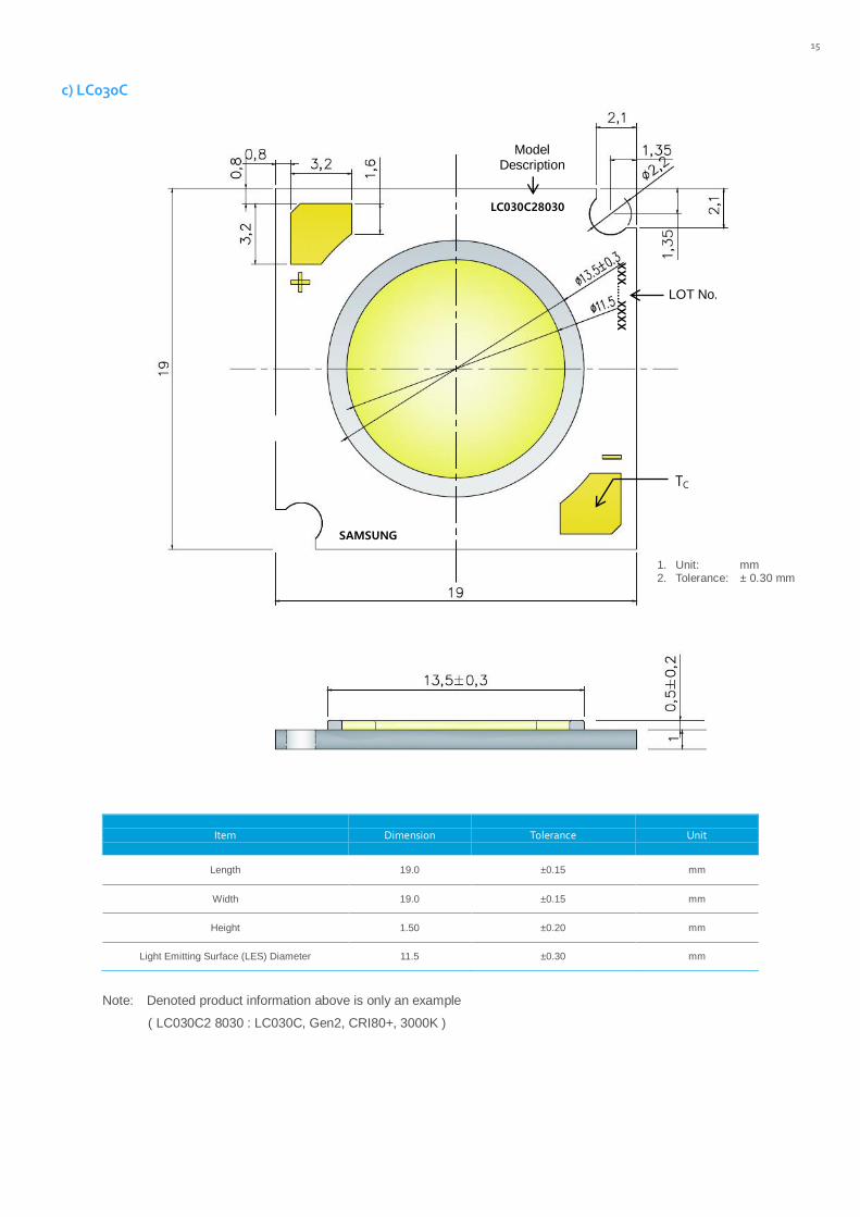
c) LC030C
Item Dimension Tolerance Unit
Length 19.0 ±0.15 mm
Width 19.0 ±0.15 mm
Height 1.50 ±0.20 mm
Light Emitting Surface (LES) Diameter 11.5 ±0.30 mm
Note: Denoted product information above is only an example
( LC030C2 8030 : LC030C, Gen2, CRI80+, 3000K )
SAMSUNG
Model Description
LOT No.
LC030C28030
XXX.....X
XXX
TC
1. Unit: mm 2. Tolerance: ± 0.30 mm
16
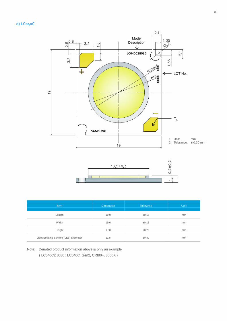
d) LC040C
Item Dimension Tolerance Unit
Length 19.0 ±0.15 mm
Width 19.0 ±0.15 mm
Height 1.50 ±0.20 mm
Light Emitting Surface (LES) Diameter 11.5 ±0.30 mm
Note: Denoted product information above is only an example
( LC040C2 8030 : LC040C, Gen2, CRI80+, 3000K )
1. Unit: mm
2. Tolerance: ± 0.30 mm
SAMSUNG
TC
LC040C28030
Model Description
XXX.....X
XXX
LOT No.
17
Bin Code
Lot Number
Product Code
YZW3C2
SPHWHAHDNC25YZW3C2 YZW3C2 01
IIIIIIIIIIIIIIIIIIIIIIIIIIIIIIIIIIIIIIIIIIIIIIIII G7AZC4001 / 1001 / xxxx pcs
IIIIIIIIIIIIIIIIIIIIIIIIIIIIIIIIIIIIIIIIII
YZW3C2
SPHWHAHDNC25YZW3C2 YZW3C2 01
IIIIIIIIIIIIIIIIIIIIIIIIIIIIIIIIIIIIIIIIIIIIIIIII ①②③④⑤⑥⑦⑧⑨/1ⓐⓑⓒ/ xxxx pcs
IIIIIIIIIIIIIIIIIIIIIIIIIIIIIIIIIIIIIIIIII
5. Label Structure
a) Label Structure
Note: Denoted bin code and product code above is only an example (see description on page 5)
Bin Code:
ⓐⓑ: Forward Voltage bin (refer to page 11)
ⓒⓓ: Chromaticity bin (refer to page 9-10)
ⓔⓕ: Luminous Flux bin (refer to page 6)
b) Lot Number
The lot number is composed of the following characters:
① ③④⑤⑥⑦⑧⑨ / 1ⓐⓑⓒ / xxxx pcs
① : Production site (S: Giheung, Korea, G: Tianjin, China)
② : 7 (LED)
③ : Product state (A: Normal, B: Bulk, C: First Production, R: Reproduction, S: Sample)
④ : Year (Z: 2015, A: 2016, B: 2017…)
⑤ : Month (1~9, A, B, C)
⑥⑦⑧⑨ : Day (1~9, A, B~V)
ⓐⓑⓒ : Product serial number (001 ~ 999)
ⓐⓑⓒⓓⓔⓕ
18
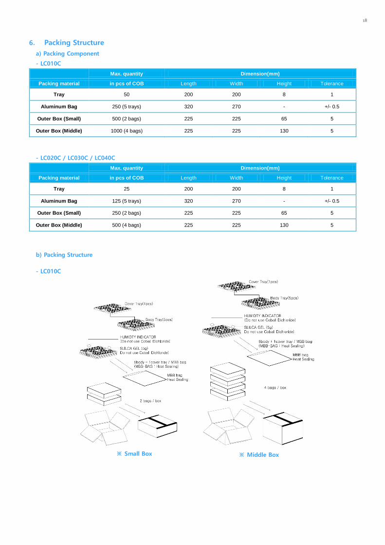
6. Packing Structure
a) Packing Component
- LC010C
Max. quantity Dimension(mm)
Packing material in pcs of COB Length Width Height Tolerance
Tray 50 200 200 8 1
Aluminum Bag 250 (5 trays) 320 270 - +/- 0.5
Outer Box (Small) 500 (2 bags) 225 225 65 5
Outer Box (Middle) 1000 (4 bags) 225 225 130 5
- LC020C / LC030C / LC040C
Max. quantity Dimension(mm)
Packing material in pcs of COB Length Width Height Tolerance
Tray 25 200 200 8 1
Aluminum Bag 125 (5 trays) 320 270 - +/- 0.5
Outer Box (Small) 250 (2 bags) 225 225 65 5
Outer Box (Middle) 500 (4 bags) 225 225 130 5
b) Packing Structure
- LC010C
※ Small Box ※ Middle Box
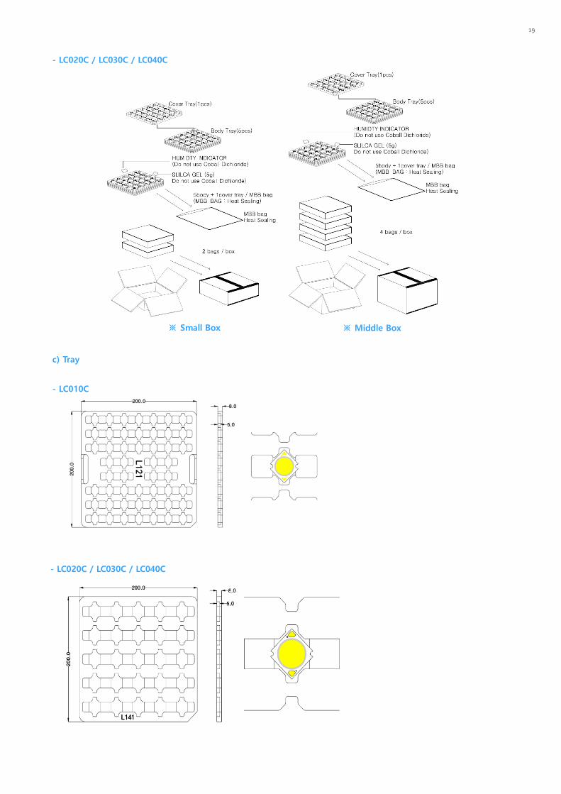
19
- LC020C / LC030C / LC040C
c) Tray
- LC010C
- LC020C / LC030C / LC040C
※ Small Box ※ Middle Box

20
7. Precautions in Handling & Use
1) This device should not be used in any type of fluid such as water, oil, organic solvent, etc. When cleaning is required, IPA
is recommended as the cleaning agent. Some solvent-based cleaning agent may damage the silicone resins used in the
device.
2) LEDs must be stored in a clean environment. If the LEDs are to be stored for three months or more after being shipped
from Samsung, they should be packed with a nitrogen-filled container (shelf life of sealed bags is 12 months at
temperature 0~40 ºC, 0~90 % RH).
3) After storage bag is opened, device subjected to soldering, solder reflow, or other high temperature processes must be:
a. Mounted within 672 hours (28 days) at an assembly line with a condition of no more than 30 ºC / 60 % RH, or
b. Stored at <10 % RH
4) Repack unused products with anti-moisture packing, fold to close any opening and then store in a dry place.
5) Devices require baking before mounting, if humidity card reading is >60 % at 23 ± 5 ºC.
6) Devices must be baked for 1 hour at 60 ± 5 ºC, if baking is required.
7) The LEDs are sensitive to the static electricity and surge current. It is recommended to use a wrist band or anti-
electrostatic glove when handling the LEDs. If voltage exceeding the absolute maximum rating is applied to LEDs, it may
cause damage or even destruction to LED devices. Damaged LEDs may show some unusual characteristics such as
increase in leakage current, lowered turn-on voltage, or abnormal lighting of LEDs at low current.
8) The thermal management is one of the most critical factors for the LED lighting system. Especially the LED junction
temperature should not exceed the absolute maximum rating while operation of LED lighting system.
For more information, please refer to Application Note ‘Mechanical & Thermal Guide for COB’.
9) In case of driving LEDs around the minimum current level (If_min), chips might exhibit different brightness due to the
variation in I-V characteristics of each one. This is normal and does not adversely affect the performance of product.
10) VOCs (Volatile Organic Compounds) can be generated from adhesives, flux, hardener or organic additives used in
luminaires (fixtures). Transparent LED silicone encapsulant is permeable to those chemicals and they may lead to a
discoloration of encapsulant when they exposed to heat or light. This phenomenon can cause a significant loss of light
emitted (output) from the luminaires. In order to prevent these problems, we recommend users to know the physical
properties of materials used in luminaires and they must be carefully selected.
11) The resin area is very sensitive, please do not handle, press, touch, rub, clean, or pick by with tweezers on it. Instead,
please pick at the handling area as indicated below.

Legal and additional information.
About Samsung Electronics Co., Ltd.
Samsung Electronics Co., Ltd. inspires the world and shapes the future
with transformative ideas and technologies, redefining the worlds of TVs,
smartphones, wearable devices, tablets, cameras, digital appliances,
printers, medical equipment, network systems and semiconductors.
We are also leading in the Internet of Things space through, among others,
our Digital Health and Smart Home initiatives. We employ 307,000 people
across 84 countries. To discover more, please visit our official website at
www.samsung.com and our official blog at global.samsungtomorrow.com.
Copyright © 2015 Samsung Electronics Co., Ltd. All rights reserved.
Samsung is a registered trademark of Samsung Electronics Co., Ltd.
Specifications and designs are subject to change without notice. Non-metric
weights and measurements are approximate. All data were deemed correct
at time of creation. Samsung is not liable for errors or omissions. All brand,
product, service names and logos are trademarks and/or registered trademarks
of their respective owners and are hereby recognized and acknowledged.
Samsung Electronics Co., Ltd.
95, Samsung 2-ro
Giheung-gu
Yongin-si, Gyeonggi-do, 446-711
KOREA
www.samsungled.com


![LUXEON CoB with CrispWhite Technology (Gen 2)...LUXEON CoB with CrispWhite Technology (Gen 2) product performance at specified test current, T j =85 C. PRODUCT NOMINAL [4] CCT MINIMUM](https://static.fdocuments.net/doc/165x107/5fe1d233c14cca231711d4b7/luxeon-cob-with-crispwhite-technology-gen-2-luxeon-cob-with-crispwhite-technology.jpg)