< Silicon RF Power MOS FET (Discrete) > RD70HUP2...< Silicon RF Power MOS FET (Discrete) > RD70HUP2...
19
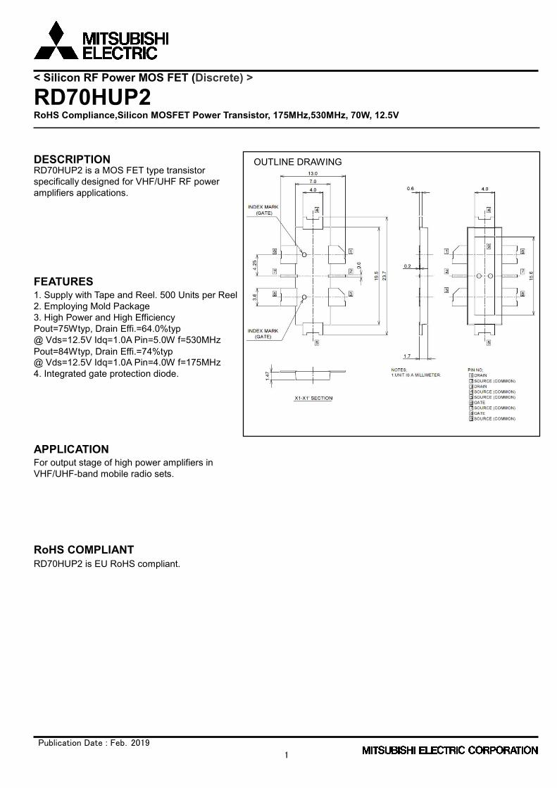
Publication Date : Feb.2019 1 OUTLINE DRAWING < Silicon RF Power MOS FET (Discrete) > RD70HUP2 RoHS Compliance,Silicon MOSFET Power Transistor, 175MHz,530MHz, 70W, 12.5V DESCRIPTION RD70HUP2 is a MOS FET type transistor specifically designed for VHF/UHF RF power amplifiers applications. FEATURES 1. Supply with Tape and Reel. 500 Units per Reel 2. Employing Mold Package 3. High Power and High Efficiency Pout=75Wtyp, Drain Effi.=64.0%typ @ Vds=12.5V Idq=1.0A Pin=5.0W f=530MHz Pout=84Wtyp, Drain Effi.=74%typ @ Vds=12.5V Idq=1.0A Pin=4.0W f=175MHz 4. Integrated gate protection diode. APPLICATION For output stage of high power amplifiers in VHF/UHF-band mobile radio sets. RoHS COMPLIANT RD70HUP2 is EU RoHS compliant.
Transcript of < Silicon RF Power MOS FET (Discrete) > RD70HUP2...< Silicon RF Power MOS FET (Discrete) > RD70HUP2...
Publication Date : Feb.2019
1
OUTLINE DRAWING
< Silicon RF Power MOS FET (Discrete) >
RD70HUP2 RoHS Compliance,Silicon MOSFET Power Transistor, 175MHz,530MHz, 70W, 12.5V DESCRIPTION RD70HUP2 is a MOS FET type transistor specifically designed for VHF/UHF RF power amplifiers applications.
FEATURES 1. Supply with Tape and Reel. 500 Units per Reel 2. Employing Mold Package 3. High Power and High Efficiency Pout=75Wtyp, Drain Effi.=64.0%typ @ Vds=12.5V Idq=1.0A Pin=5.0W f=530MHz Pout=84Wtyp, Drain Effi.=74%typ @ Vds=12.5V Idq=1.0A Pin=4.0W f=175MHz 4. Integrated gate protection diode.
APPLICATION For output stage of high power amplifiers in VHF/UHF-band mobile radio sets.
RoHS COMPLIANT RD70HUP2 is EU RoHS compliant.
< Silicon RF Power MOS FET (Discrete) >
RD70HUP2 RoHS Compliance,Silicon MOSFET Power Transistor, 175MHz,530MHz, 70W, 12.5V
Publication Date : Feb.2019
2
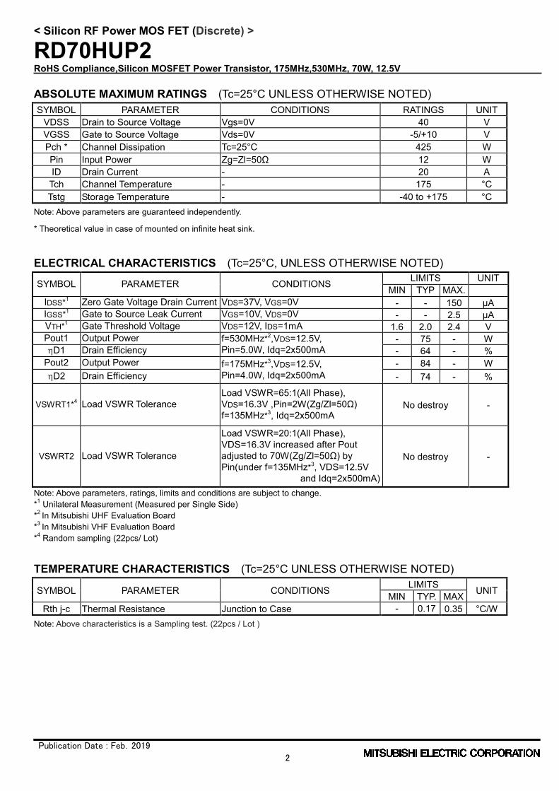
ABSOLUTE MAXIMUM RATINGS (Tc=25°C UNLESS OTHERWISE NOTED) SYMBOL PARAMETER CONDITIONS RATINGS UNIT
VDSS Drain to Source Voltage Vgs=0V 40 V VGSS Gate to Source Voltage Vds=0V -5/+10 V Pch * Channel Dissipation Tc=25°C 425 W Pin Input Power Zg=Zl=50Ω 12 W ID Drain Current - 20 A Tch Channel Temperature - 175 °C Tstg Storage Temperature - -40 to +175 °C
Note: Above parameters are guaranteed independently.
* Theoretical value in case of mounted on infinite heat sink.
ELECTRICAL CHARACTERISTICS (Tc=25°C, UNLESS OTHERWISE NOTED)
SYMBOL PARAMETER CONDITIONS LIMITS UNIT MIN TYP MAX.
IDSS*1 Zero Gate Voltage Drain Current VDS=37V, VGS=0V - - 150 μA IGSS*1 Gate to Source Leak Current VGS=10V, VDS=0V - - 2.5 μA VTH*1 Gate Threshold Voltage VDS=12V, IDS=1mA 1.6 2.0 2.4 V Pout1 Output Power f=530MHz*2,VDS=12.5V,
Pin=5.0W, Idq=2x500mA - 75 - W
D1 Drain Efficiency - 64 - % Pout2 Output Power f=175MHz*3,VDS=12.5V,
Pin=4.0W, Idq=2x500mA - 84 - W
D2 Drain Efficiency - 74 - %
VSWRT1*4 Load VSWR Tolerance Load VSWR=65:1(All Phase), VDS=16.3V ,Pin=2W(Zg/Zl=50Ω) f=135MHz*3, Idq=2x500mA
No destroy -
VSWRT2 Load VSWR Tolerance
Load VSWR=20:1(All Phase), VDS=16.3V increased after Pout adjusted to 70W(Zg/Zl=50Ω) by Pin(under f=135MHz*3, VDS=12.5V
and Idq=2x500mA)
No destroy -
Note: Above parameters, ratings, limits and conditions are subject to change. *1 Unilateral Measurement (Measured per Single Side) *2 In Mitsubishi UHF Evaluation Board *3 In Mitsubishi VHF Evaluation Board *4 Random sampling (22pcs/ Lot)
TEMPERATURE CHARACTERISTICS (Tc=25°C UNLESS OTHERWISE NOTED)
SYMBOL PARAMETER CONDITIONS LIMITS UNIT MIN TYP. MAX Rth j-c Thermal Resistance Junction to Case - 0.17 0.35 °C/W
Note: Above characteristics is a Sampling test. (22pcs / Lot )
< Silicon RF Power MOS FET (Discrete) >
RD70HUP2 RoHS Compliance,Silicon MOSFET Power Transistor, 175MHz,530MHz, 70W, 12.5V
Publication Date : Feb.2019
3
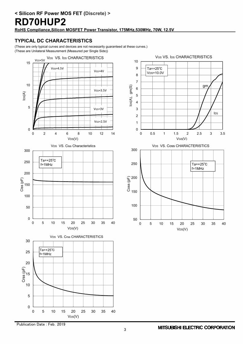
TYPICAL DC CHARACTERISTICS (These are only typical curves and devices are not necessarily guaranteed at these curves.) (These are Unilateral Measurement (Measured per Single Side))
0
1
2
3
4
5
6
7
8
9
10
0 0.5 1 1.5 2 2.5 3 3.5ID
S(A)
,gm
(S)
VGS(V)
VGS VS. IDS CHARACTERISTICS
gm
IDS
Ta=+25℃VDS=10.0V
0
50
100
150
200
250
300
0 5 10 15 20 25 30 35 40
Cis
s (p
F)
VDS(V)
VDS VS. Ciss Characteristics
Ta=+25℃f=1MHz
50
100
150
200
250
300
0 5 10 15 20 25 30 35 40
Cos
s (p
F)
VDS(V)
VDS VS. Coss CHARACTERISTICS
Ta=+25℃f=1MHz
0
5
10
15
20
25
30
0 5 10 15 20 25 30 35 40
Crs
s (p
F)
VDS(V)
VDS VS. Crss CHARACTERISTICS
Ta=+25℃f=1MHz
0
5
10
15
0 2 4 6 8 10 12 14
IDS(
A)
VDS(V)
VDS VS. IDS CHARACTERISTICSVGS=5V
VGs=4.5VVGS=4V
VGS=3.5V
VGS=3V
VGS=2.5V
< Silicon RF Power MOS FET (Discrete) >
RD70HUP2 RoHS Compliance,Silicon MOSFET Power Transistor, 175MHz,530MHz, 70W, 12.5V
Publication Date : Feb.2019
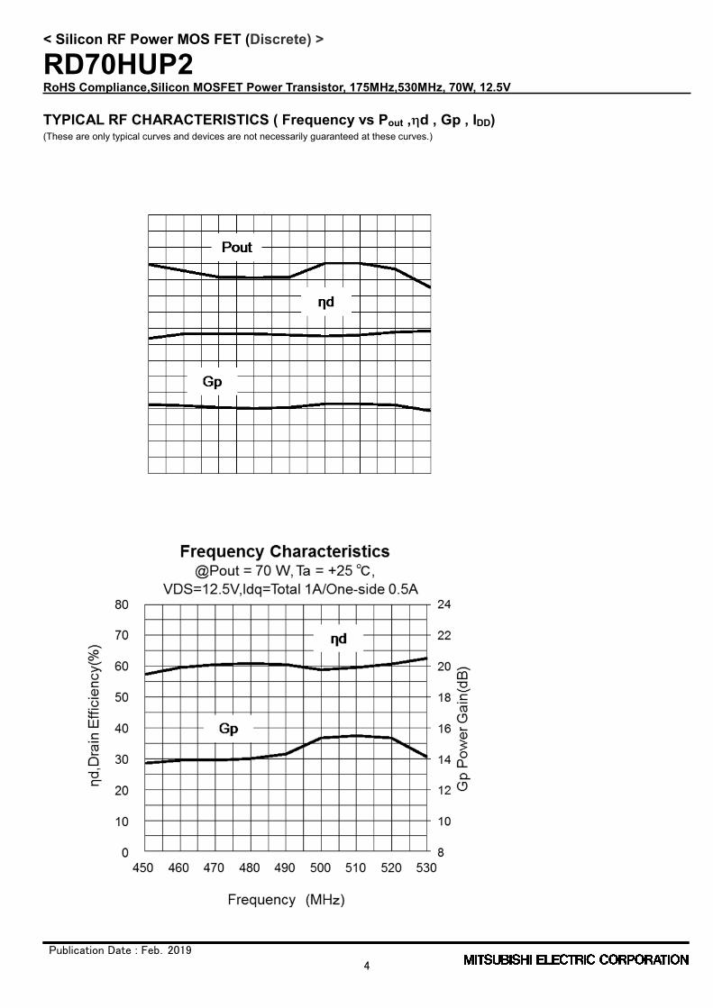
4
TYPICAL RF CHARACTERISTICS ( Frequency vs Pout , d , Gp , IDD) (These are only typical curves and devices are not necessarily guaranteed at these curves.)
< Silicon RF Power MOS FET (Discrete) >
RD70HUP2 RoHS Compliance,Silicon MOSFET Power Transistor, 175MHz,530MHz, 70W, 12.5V
Publication Date : Feb.2019
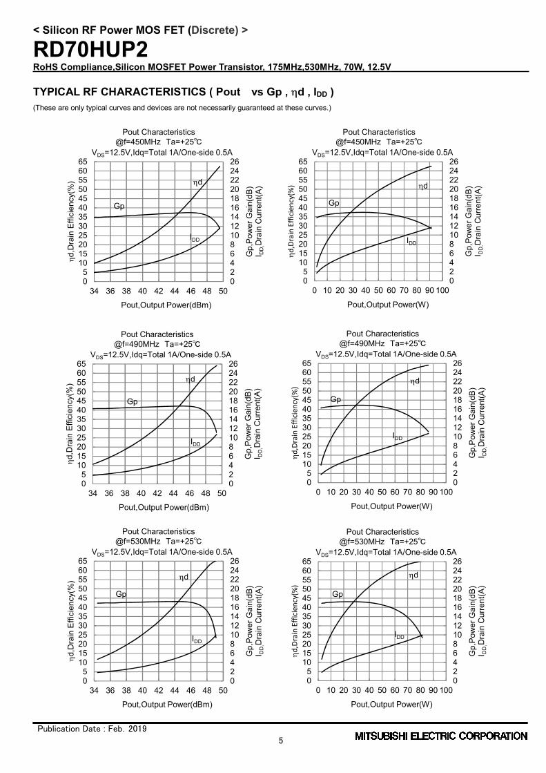
5
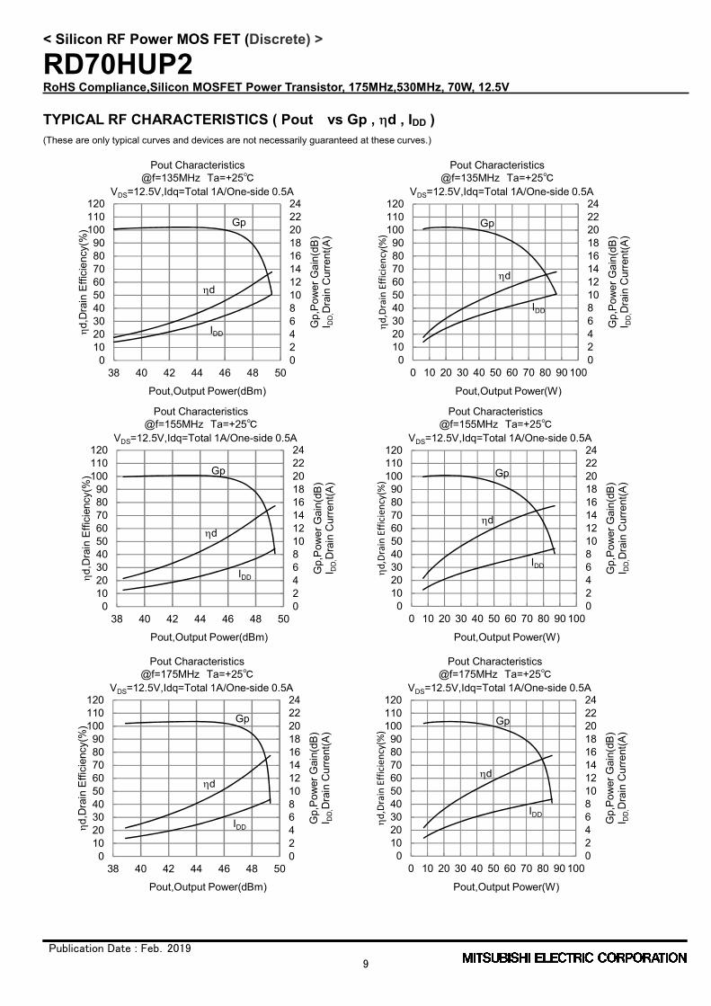
TYPICAL RF CHARACTERISTICS ( Pout vs Gp , d , IDD ) (These are only typical curves and devices are not necessarily guaranteed at these curves.)
02468101214161820222426
05
101520253035404550556065
34 36 38 40 42 44 46 48 50
Gp,
Pow
er G
ain(
dB)
I DD
,Dra
in C
urre
nt(A
)
hd,D
rain
Effi
cien
cy(%
)
Pout,Output Power(dBm)
Pout Characteristics@f=450MHz Ta=+25℃
VDS=12.5V,Idq=Total 1A/One-side 0.5A
IDD
Gp
hd
02468101214161820222426
05
101520253035404550556065
0 10 20 30 40 50 60 70 80 90 100
Gp,
Pow
er G
ain(
dB)
I DD
,Dra
in C
urre
nt(A
)
hd,D
rain
Effi
cienc
y(%
)
Pout,Output Power(W)
Pout Characteristics@f=450MHz Ta=+25℃
VDS=12.5V,Idq=Total 1A/One-side 0.5A
hd
IDD
Gp
02468101214161820222426
05
101520253035404550556065
34 36 38 40 42 44 46 48 50
Gp,
Pow
er G
ain(
dB)
I DD
,Dra
in C
urre
nt(A
)
hd,D
rain
Effi
cien
cy(%
)
Pout,Output Power(dBm)
Pout Characteristics@f=490MHz Ta=+25℃
VDS=12.5V,Idq=Total 1A/One-side 0.5A
IDD
Gp
hd
02468101214161820222426
05
101520253035404550556065
0 10 20 30 40 50 60 70 80 90 100
Gp,
Pow
er G
ain(
dB)
I DD
,Dra
in C
urre
nt(A
)
hd,D
rain
Effi
cienc
y(%
)
Pout,Output Power(W)
Pout Characteristics@f=490MHz Ta=+25℃
VDS=12.5V,Idq=Total 1A/One-side 0.5A
hd
IDD
Gp
02468101214161820222426
05
101520253035404550556065
34 36 38 40 42 44 46 48 50
Gp,
Pow
er G
ain(
dB)
I DD
,Dra
in C
urre
nt(A
)
hd,D
rain
Effi
cien
cy(%
)
Pout,Output Power(dBm)
Pout Characteristics@f=530MHz Ta=+25℃
VDS=12.5V,Idq=Total 1A/One-side 0.5A
IDD
Gp
hd
02468101214161820222426
05
101520253035404550556065
0 10 20 30 40 50 60 70 80 90 100
Gp,
Pow
er G
ain(
dB)
I DD
,Dra
in C
urre
nt(A
)
hd,D
rain
Effi
cienc
y(%
)
Pout,Output Power(W)
Pout Characteristics@f=530MHz Ta=+25℃
VDS=12.5V,Idq=Total 1A/One-side 0.5A
hd
IDD
Gp
< Silicon RF Power MOS FET (Discrete) >
RD70HUP2 RoHS Compliance,Silicon MOSFET Power Transistor, 175MHz,530MHz, 70W, 12.5V
Publication Date : Feb.2019
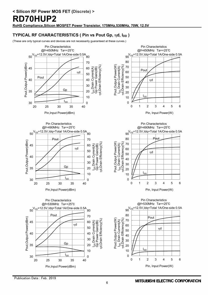
6
TYPICAL RF CHARACTERISTICS ( Pin vs Pout Gp, d, IDD ) (These are only typical curves and devices are not necessarily guaranteed at these curves.)
0102030405060708090
0 1 2 3 4 5 6
Pout
,Out
put P
ower
(W)
I DD
, Dra
in C
urre
nt(A
)hd
,Dra
in E
ffici
ency
(%)
Pin, Input Power(W)
Pin Characteristics@f=450MHz Ta=+25℃
VDS=12.5V,Idq=Total 1A/One-side 0.5A
Pout
hd
IDD
0
10
20
30
40
50
60
70
80
30
35
40
45
50
20 25 30 35 40
I DD
,Dra
in C
urre
nt(A
)G
p Po
wer
Gai
n(dB
)hd
,Dra
in E
ffici
ency
(%)
Pout
,Out
put P
ower
(dBm
)
Pin,Input Power(dBm)
Pin Characteristics@f=450MHz Ta=+25℃
VDS=12.5V,Idq=Total 1A/One-side 0.5A
IDD
Gp
Pouthd
0
10
20
30
40
50
60
70
80
30
35
40
45
50
20 25 30 35 40
I DD
,Dra
in C
urre
nt(A
)G
p Po
wer
Gai
n(dB
)hd
,Dra
in E
ffici
ency
(%)
Pout
,Out
put P
ower
(dBm
)
Pin,Input Power(dBm)
Pin Characteristics@f=490MHz Ta=+25℃
VDS=12.5V,Idq=Total 1A/One-side 0.5A
IDD
Gp
Pout
hd
0102030405060708090
0 1 2 3 4 5 6
Pout
,Out
put P
ower
(W)
I DD
, Dra
in C
urre
nt(A
)hd
,Dra
in E
ffici
ency
(%)
Pin, Input Power(W)
Pin Characteristics@f=490MHz Ta=+25℃
VDS=12.5V,Idq=Total 1A/One-side 0.5A
Pout
hd
IDD
0
10
20
30
40
50
60
70
80
30
35
40
45
50
20 25 30 35 40
I DD
,Dra
in C
urre
nt(A
)G
p Po
wer
Gai
n(dB
)hd
,Dra
in E
ffici
ency
(%)
Pout
,Out
put P
ower
(dBm
)
Pin,Input Power(dBm)
Pin Characteristics@f=530MHz Ta=+25℃
VDS=12.5V,Idq=Total 1A/One-side 0.5A
IDD
Gp
Pout
hd
0102030405060708090
0 1 2 3 4 5 6
Pout
,Out
put P
ower
(W)
I DD
, Dra
in C
urre
nt(A
)hd
,Dra
in E
ffici
ency
(%)
Pin, Input Power(W)
Pin Characteristics@f=530MHz Ta=+25℃
VDS=12.5V,Idq=Total 1A/One-side 0.5A
Pout
hd
IDD
< Silicon RF Power MOS FET (Discrete) >
RD70HUP2 RoHS Compliance,Silicon MOSFET Power Transistor, 175MHz,530MHz, 70W, 12.5V
Publication Date : Feb.2019
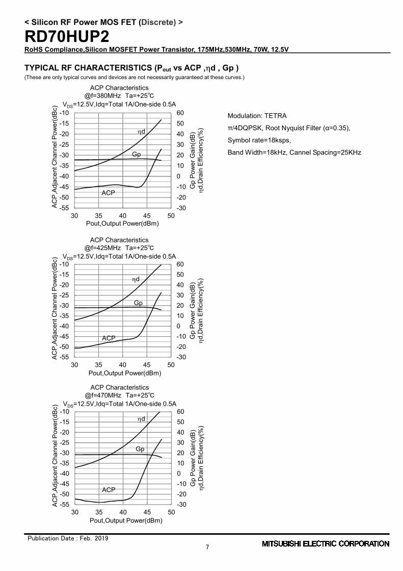
7
TYPICAL RF CHARACTERISTICS (Pout vs ACP , d , Gp ) (These are only typical curves and devices are not necessarily guaranteed at these curves.)
-30-20-100102030405060
-55-50-45-40-35-30-25-20-15-10
30 35 40 45 50
Gp
Pow
er G
ain(
dB)
hd,D
rain
Effi
cien
cy(%
)
ACP,
Adj
acen
t Cha
nnel
Pow
er(d
Bc)
Pout,Output Power(dBm)
hd
Gp
ACP Characteristics@f=425MHz Ta=+25℃
VDS=12.5V,Idq=Total 1A/One-side 0.5A
ACP
-30-20-100102030405060
-55-50-45-40-35-30-25-20-15-10
30 35 40 45 50
Gp
Pow
er G
ain(
dB)
hd,D
rain
Effi
cien
cy(%
)
ACP,
Adja
cent
Cha
nnel
Pow
er(d
Bc)
Pout,Output Power(dBm)
hd
Gp
ACP Characteristics@f=380MHz Ta=+25℃
VDS=12.5V,Idq=Total 1A/One-side 0.5A
ACP
-30-20-100102030405060
-55-50-45-40-35-30-25-20-15-10
30 35 40 45 50
Gp
Pow
er G
ain(
dB)
hd,D
rain
Effi
cien
cy(%
)
ACP,
Adja
cent
Cha
nnel
Pow
er(d
Bc)
Pout,Output Power(dBm)
hd
Gp
ACP Characteristics@f=470MHz Ta=+25℃
VDS=12.5V,Idq=Total 1A/One-side 0.5A
ACP
Modulation: TETRA
π/4DQPSK, Root Nyquist Filter (α=0.35),
Symbol rate=18ksps,
Band Width=18kHz, Cannel Spacing=25KHz
< Silicon RF Power MOS FET (Discrete) >
RD70HUP2 RoHS Compliance,Silicon MOSFET Power Transistor, 175MHz,530MHz, 70W, 12.5V
Publication Date : Feb.2019
8
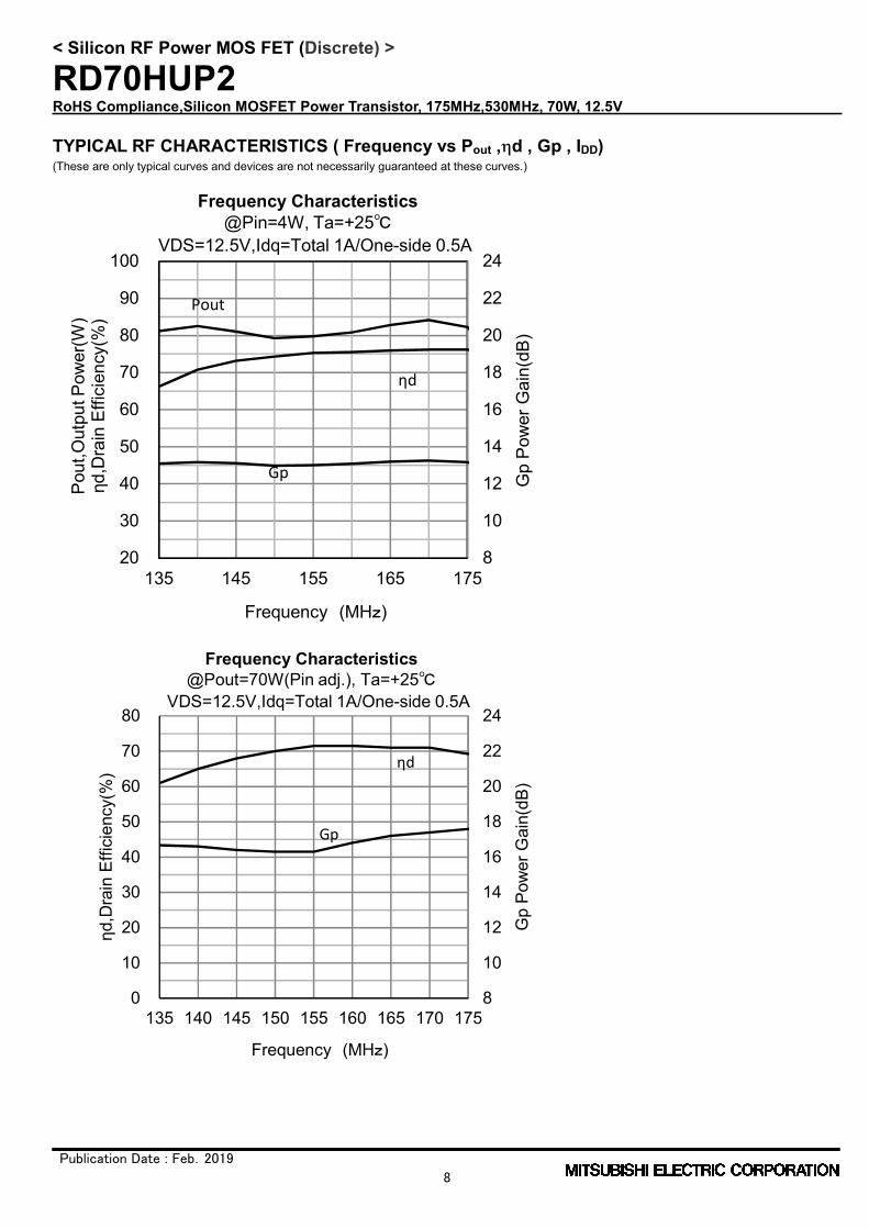
TYPICAL RF CHARACTERISTICS ( Frequency vs Pout , d , Gp , IDD) (These are only typical curves and devices are not necessarily guaranteed at these curves.)
8
10
12
14
16
18
20
22
24
20
30
40
50
60
70
80
90
100
135 145 155 165 175
Gp
Pow
er G
ain(
dB)
Pout
,Out
put P
ower
(W)
ηd,D
rain
Effi
cien
cy(%
)
Frequency (MHz)
Frequency Characteristics@Pin=4W, Ta=+25℃
VDS=12.5V,Idq=Total 1A/One-side 0.5A
Pout
ηd
Gp
8
10
12
14
16
18
20
22
24
0
10
20
30
40
50
60
70
80
135 140 145 150 155 160 165 170 175
Gp
Pow
er G
ain(
dB)
ηd,D
rain
Effi
cien
cy(%
)
Frequency (MHz)
Frequency Characteristics@Pout=70W(Pin adj.), Ta=+25℃
VDS=12.5V,Idq=Total 1A/One-side 0.5A
ηd
Gp
< Silicon RF Power MOS FET (Discrete) >
RD70HUP2 RoHS Compliance,Silicon MOSFET Power Transistor, 175MHz,530MHz, 70W, 12.5V
Publication Date : Feb.2019
9
TYPICAL RF CHARACTERISTICS ( Pout vs Gp , d , IDD ) (These are only typical curves and devices are not necessarily guaranteed at these curves.)
024681012141618202224
0102030405060708090
100110120
38 40 42 44 46 48 50
Gp,
Pow
er G
ain(
dB)
I DD
,Dra
in C
urre
nt(A
)
hd,D
rain
Effi
cien
cy(%
)
Pout,Output Power(dBm)
Pout Characteristics@f=135MHz Ta=+25℃
VDS=12.5V,Idq=Total 1A/One-side 0.5A
IDD
Gp
hd
024681012141618202224
0102030405060708090
100110120
0 10 20 30 40 50 60 70 80 90 100
Gp,
Pow
er G
ain(
dB)
I DD
,Dra
in C
urre
nt(A
)
hd,D
rain
Effi
cienc
y(%
)Pout,Output Power(W)
Pout Characteristics@f=135MHz Ta=+25℃
VDS=12.5V,Idq=Total 1A/One-side 0.5A
hd
IDD
Gp
024681012141618202224
0102030405060708090
100110120
0 10 20 30 40 50 60 70 80 90 100G
p,Po
wer
Gai
n(dB
)I D
D,D
rain
Cur
rent
(A)
hd,D
rain
Effi
cienc
y(%
)
Pout,Output Power(W)
Pout Characteristics@f=155MHz Ta=+25℃
VDS=12.5V,Idq=Total 1A/One-side 0.5A
hd
IDD
Gp
024681012141618202224
0102030405060708090
100110120
0 10 20 30 40 50 60 70 80 90 100
Gp,
Pow
er G
ain(
dB)
I DD
,Dra
in C
urre
nt(A
)
hd,D
rain
Effi
cienc
y(%
)
Pout,Output Power(W)
Pout Characteristics@f=175MHz Ta=+25℃
VDS=12.5V,Idq=Total 1A/One-side 0.5A
hd
IDD
Gp
024681012141618202224
0102030405060708090
100110120
38 40 42 44 46 48 50
Gp,
Pow
er G
ain(
dB)
I DD
,Dra
in C
urre
nt(A
)
hd,D
rain
Effi
cien
cy(%
)
Pout,Output Power(dBm)
Pout Characteristics@f=175MHz Ta=+25℃
VDS=12.5V,Idq=Total 1A/One-side 0.5A
IDD
Gp
hd
024681012141618202224
0102030405060708090
100110120
38 40 42 44 46 48 50
Gp,
Pow
er G
ain(
dB)
I DD
,Dra
in C
urre
nt(A
)
hd,D
rain
Effi
cien
cy(%
)
Pout,Output Power(dBm)
Pout Characteristics@f=155MHz Ta=+25℃
VDS=12.5V,Idq=Total 1A/One-side 0.5A
IDD
Gp
hd
< Silicon RF Power MOS FET (Discrete) >
RD70HUP2 RoHS Compliance,Silicon MOSFET Power Transistor, 175MHz,530MHz, 70W, 12.5V
Publication Date : Feb.2019
10
TYPICAL RF CHARACTERISTICS ( Pin vs Pout Gp, d, IDD ) (These are only typical curves and devices are not necessarily guaranteed at these curves.)
0
10
20
30
40
50
60
70
80
30
35
40
45
50
20 25 30 35 40
I DD
,Dra
in C
urre
nt(A
)G
p Po
wer
Gai
n(dB
)hd
,Dra
in E
ffici
ency
(%)
Pout
,Out
put P
ower
(dBm
)
Pin,Input Power(dBm)
Pin Characteristics@f=135MHz Ta=+25℃
VDS=12.5V,Idq=Total 1A/One-side 0.5A
IDD
Gp
Pout
hd
0102030405060708090
0 1 2 3 4 5 6
Pout
,Out
put P
ower
(W)
I DD
, Dra
in C
urre
nt(A
)hd
,Dra
in E
ffici
ency
(%)
Pin, Input Power(W)
Pin Characteristics@f=135MHz Ta=+25℃
VDS=12.5V,Idq=Total 1A/One-side 0.5A
Pout
hd
IDD
0102030405060708090
0 1 2 3 4 5 6
Pout
,Out
put P
ower
(W)
I DD
, Dra
in C
urre
nt(A
)hd
,Dra
in E
ffici
ency
(%)
Pin, Input Power(W)
Pin Characteristics@f=155MHz Ta=+25℃
VDS=12.5V,Idq=Total 1A/One-side 0.5A
Pout
hd
IDD
0
10
20
30
40
50
60
70
80
30
35
40
45
50
20 25 30 35 40
I DD
,Dra
in C
urre
nt(A
)G
p Po
wer
Gai
n(dB
)hd
,Dra
in E
ffici
ency
(%)
Pout
,Out
put P
ower
(dBm
)
Pin,Input Power(dBm)
Pin Characteristics@f=175MHz Ta=+25℃
VDS=12.5V,Idq=Total 1A/One-side 0.5A
IDD
Gp
Pout
hd
0102030405060708090
0 1 2 3 4 5 6
Pout
,Out
put P
ower
(W)
I DD
, Dra
in C
urre
nt(A
)hd
,Dra
in E
ffici
ency
(%)
Pin, Input Power(W)
Pin Characteristics@f=175MHz Ta=+25℃
VDS=12.5V,Idq=Total 1A/One-side 0.5A
Pout
hd
IDD
0
10
20
30
40
50
60
70
80
30
35
40
45
50
20 25 30 35 40
I DD
,Dra
in C
urre
nt(A
)G
p Po
wer
Gai
n(dB
)hd
,Dra
in E
ffici
ency
(%)
Pout
,Out
put P
ower
(dBm
)
Pin,Input Power(dBm)
Pin Characteristics@f=155MHz Ta=+25℃
VDS=12.5V,Idq=Total 1A/One-side 0.5A
IDD
Gp
Pouthd
< Silicon RF Power MOS FET (Discrete) >
RD70HUP2 RoHS Compliance,Silicon MOSFET Power Transistor, 175MHz,530MHz, 70W, 12.5V
Publication Date : Feb.2019
11
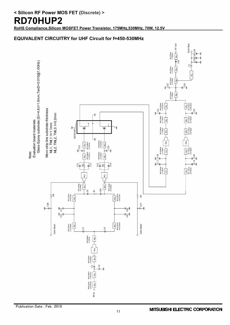
EQUIVALENT CIRCUITRY for UHF Circuit for f=450-530MHz
Note
: E
valu
atio
n bo
ard
mat
eria
ls
Gla
ss-E
poxy
sub
stra
te (E
r=4.
8,t=
1.5m
m,T
anD
=0.0
15@
1.0G
Hz)
Mic
ro s
trip
line
subs
trate
thic
knes
s
M
L1, T
ML1
: t=1
.1m
m
M
L2, T
ML2
, TM
L3: t
=0.2
mm
< Silicon RF Power MOS FET (Discrete) >
RD70HUP2 RoHS Compliance,Silicon MOSFET Power Transistor, 175MHz,530MHz, 70W, 12.5V
Publication Date : Feb.2019
12
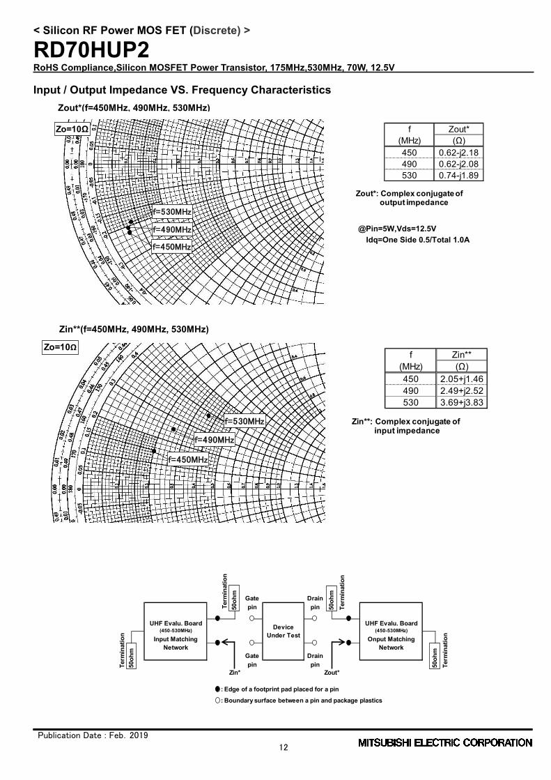
Input / Output Impedance VS. Frequency Characteristics
Gate Drainpin pin
UHF Evalu. Board UHF Evalu. Board
Input Matching Onput MatchingNetwork Network
Gate Drainpin pin
: Edge of a footprint pad placed for a pin
: Boundary surface between a pin and package plastics
Zin* Zout*
(450-530MHz) (450-530MHz)DeviceUnder Test
50oh
mTe
rmin
atio
n
50oh
mTe
rmin
atio
n
50oh
mTe
rmin
atio
n
Term
inat
ion
50oh
m
f Zout*(MHz) (Ω)450 0.62-j2.18490 0.62-j2.08530 0.74-j1.89
Zout*: Complex conjugate of output impedance
Zo=10Ω
f=450MHz
f=490MHz
f=530MHz
f Zin**(MHz) (Ω)450 2.05+j1.46490 2.49+j2.52530 3.69+j3.83
Zin**: Complex conjugate ofinput impedance
Zo=10Ω
f=450MHz
f=490MHz
f=530MHz
@Pin=5W,Vds=12.5V Idq=One Side 0.5/Total 1.0A
Zout*(f=450MHz, 490MHz, 530MHz)
Zin**(f=450MHz, 490MHz, 530MHz)

< Silicon RF Power MOS FET (Discrete) >
RD70HUP2 RoHS Compliance,Silicon MOSFET Power Transistor, 175MHz,530MHz, 70W, 12.5V
Publication Date : Feb.2019
13
EVB(Evaluation Board) for UHF COMPONENT LIST
Parts Type Symbol Description Type name VenderC 1 330 pF 3216 GRM31A5C2J331JW01D Murata Manufacturing Co.,LtdC 2 6.2 pF 1608 Hi-Q GQM1882C2A6R2DB01D Murata Manufacturing Co.,LtdC 3 100 pF 1608 Hi-Q GQM1882C1H101JB01D Murata Manufacturing Co.,LtdC 4 100 pF 1608 Hi-Q GQM1882C1H101JB01D Murata Manufacturing Co.,LtdC 5 20 pF 1608 Hi-Q GQM1882C1H200JB01D Murata Manufacturing Co.,LtdC 6 20 pF 1608 Hi-Q GQM1882C1H200JB01D Murata Manufacturing Co.,LtdC 7 9.2 pF 1608 Hi-Q GQM1882C1H9R2CB01D Murata Manufacturing Co.,LtdC 8 9.2 pF 1608 Hi-Q GQM1882C1H9R2CB01D Murata Manufacturing Co.,LtdC 9 1000 pF 1608 GRM188R11H102KA01D Murata Manufacturing Co.,LtdC 10 1000 pF 1608 GRM188R11H102KA01D Murata Manufacturing Co.,LtdC 11 100 pF 2012 Hi-Q GQM2195C2E101JB12D Murata Manufacturing Co.,LtdC 12 100 pF 2012 Hi-Q GQM2195C2E101JB12D Murata Manufacturing Co.,LtdC 13 100 pF 2012 Hi-Q GQM2195C2E101JB12D Murata Manufacturing Co.,LtdC 14 100 pF 2012 Hi-Q GQM2195C2E101JB12D Murata Manufacturing Co.,LtdC 15 18 pF 1608 Hi-Q GQM1882C1H180JB01D Murata Manufacturing Co.,LtdC 16 18 pF 1608 Hi-Q GQM1882C1H180JB01D Murata Manufacturing Co.,LtdC 17 39 pF 2012 Hi-Q GQM2195C2E390JB12D Murata Manufacturing Co.,LtdC 18 39 pF 2012 Hi-Q GQM2195C2E390JB12D Murata Manufacturing Co.,LtdC 19 33 pF 2012 Hi-Q GQM2195C2E330JB12D Murata Manufacturing Co.,LtdC 20 33 pF 2012 Hi-Q GQM2195C2E330JB12D Murata Manufacturing Co.,LtdC 21 20 pF 2012 Hi-Q GQM2195C2E200JB12D Murata Manufacturing Co.,LtdC 22 20 pF 2012 Hi-Q GQM2195C2E200JB12D Murata Manufacturing Co.,LtdC 23 6.2 pF 2012 Hi-Q GQM2195C2E6R2CB12D Murata Manufacturing Co.,LtdC 24 6.2 pF 2012 Hi-Q GQM2195C2E6R2CB12D Murata Manufacturing Co.,LtdC 25 330 pF 3216 GRM31A5C2J331JW01D Murata Manufacturing Co.,LtdC 26 1000 pF 1608 GRM188R11H102KA01D Murata Manufacturing Co.,LtdC 27 1000 pF 1608 GRM188R11H102KA01D Murata Manufacturing Co.,LtdC 28 1000 pF 2012 GRM2162C2A102JA01 Murata Manufacturing Co.,LtdC 29 1000 pF 2012 GRM2162C2A102JA01 Murata Manufacturing Co.,LtdC 30 220 μF EEUFC1V221 Panasonic CorporationR 1 2.2 Ω RPC10T2R2J Taiyosha Electiric Co.,LtdR 2 100 Ω RPC10T101J Taiyosha Electiric Co.,LtdR 3 100 Ω RPC10T101J Taiyosha Electiric Co.,LtdR 4 2.2 kΩ RPC05T222J Taiyosha Electiric Co.,LtdR 5 2.2 kΩ RPC05T222J Taiyosha Electiric Co.,Ltd
Inductance L 1 8005C YC Corporation Co.,Ltd
Capasitor
Resistance
25nH Enameled wire 5Turns,Diameter,0.8mm,
φ2.2mm(inside diameter)
Gate Bias 2 (Vgg2)
Drain Bias
RF OUT
GND
RF IN
Gate Bias 1 (Vgg1)
< Silicon RF Power MOS FET (Discrete) >
RD70HUP2 RoHS Compliance,Silicon MOSFET Power Transistor, 175MHz,530MHz, 70W, 12.5V
Publication Date : Feb.2019
14
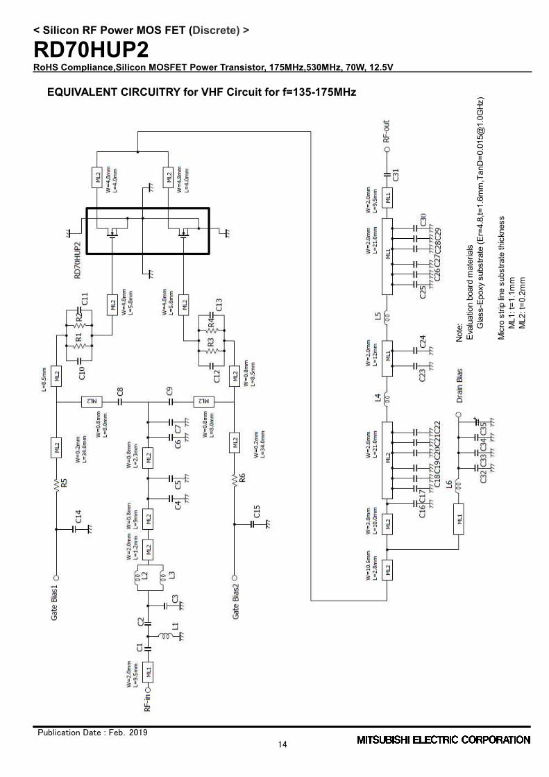
EQUIVALENT CIRCUITRY for VHF Circuit for f=135-175MHz
Note
: E
valu
atio
n bo
ard
mat
eria
ls
Gla
ss-E
poxy
sub
stra
te (E
r=4.
8,t=
1.6m
m,T
anD
=0.0
15@
1.0G
Hz)
Mic
ro s
trip
line
subs
trate
thic
knes
s
M
L1: t
=1.1
mm
ML2
: t=0
.2m
m
< Silicon RF Power MOS FET (Discrete) >
RD70HUP2 RoHS Compliance,Silicon MOSFET Power Transistor, 175MHz,530MHz, 70W, 12.5V
Publication Date : Feb.2019
15
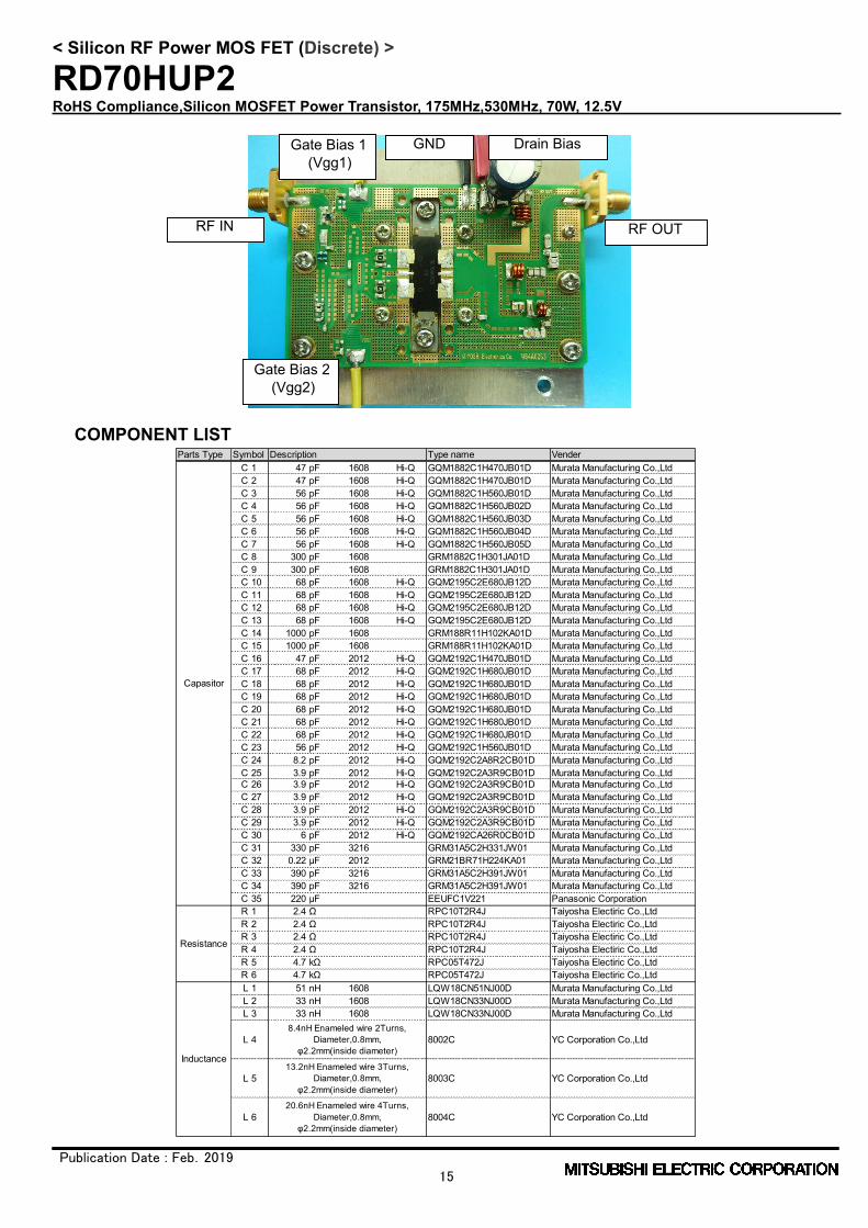
COMPONENT LIST
Gate Bias 2 (Vgg2)
Drain Bias
RF OUT
GND
RF IN
Gate Bias 1 (Vgg1)
Parts Type Symbol Description Type name VenderC 1 47 pF 1608 Hi-Q GQM1882C1H470JB01D Murata Manufacturing Co.,LtdC 2 47 pF 1608 Hi-Q GQM1882C1H470JB01D Murata Manufacturing Co.,LtdC 3 56 pF 1608 Hi-Q GQM1882C1H560JB01D Murata Manufacturing Co.,LtdC 4 56 pF 1608 Hi-Q GQM1882C1H560JB02D Murata Manufacturing Co.,LtdC 5 56 pF 1608 Hi-Q GQM1882C1H560JB03D Murata Manufacturing Co.,LtdC 6 56 pF 1608 Hi-Q GQM1882C1H560JB04D Murata Manufacturing Co.,LtdC 7 56 pF 1608 Hi-Q GQM1882C1H560JB05D Murata Manufacturing Co.,LtdC 8 300 pF 1608 GRM1882C1H301JA01D Murata Manufacturing Co.,LtdC 9 300 pF 1608 GRM1882C1H301JA01D Murata Manufacturing Co.,LtdC 10 68 pF 1608 Hi-Q GQM2195C2E680JB12D Murata Manufacturing Co.,LtdC 11 68 pF 1608 Hi-Q GQM2195C2E680JB12D Murata Manufacturing Co.,LtdC 12 68 pF 1608 Hi-Q GQM2195C2E680JB12D Murata Manufacturing Co.,LtdC 13 68 pF 1608 Hi-Q GQM2195C2E680JB12D Murata Manufacturing Co.,LtdC 14 1000 pF 1608 GRM188R11H102KA01D Murata Manufacturing Co.,LtdC 15 1000 pF 1608 GRM188R11H102KA01D Murata Manufacturing Co.,LtdC 16 47 pF 2012 Hi-Q GQM2192C1H470JB01D Murata Manufacturing Co.,LtdC 17 68 pF 2012 Hi-Q GQM2192C1H680JB01D Murata Manufacturing Co.,LtdC 18 68 pF 2012 Hi-Q GQM2192C1H680JB01D Murata Manufacturing Co.,LtdC 19 68 pF 2012 Hi-Q GQM2192C1H680JB01D Murata Manufacturing Co.,LtdC 20 68 pF 2012 Hi-Q GQM2192C1H680JB01D Murata Manufacturing Co.,LtdC 21 68 pF 2012 Hi-Q GQM2192C1H680JB01D Murata Manufacturing Co.,LtdC 22 68 pF 2012 Hi-Q GQM2192C1H680JB01D Murata Manufacturing Co.,LtdC 23 56 pF 2012 Hi-Q GQM2192C1H560JB01D Murata Manufacturing Co.,LtdC 24 8.2 pF 2012 Hi-Q GQM2192C2A8R2CB01D Murata Manufacturing Co.,LtdC 25 3.9 pF 2012 Hi-Q GQM2192C2A3R9CB01D Murata Manufacturing Co.,LtdC 26 3.9 pF 2012 Hi-Q GQM2192C2A3R9CB01D Murata Manufacturing Co.,LtdC 27 3.9 pF 2012 Hi-Q GQM2192C2A3R9CB01D Murata Manufacturing Co.,LtdC 28 3.9 pF 2012 Hi-Q GQM2192C2A3R9CB01D Murata Manufacturing Co.,LtdC 29 3.9 pF 2012 Hi-Q GQM2192C2A3R9CB01D Murata Manufacturing Co.,LtdC 30 6 pF 2012 Hi-Q GQM2192CA26R0CB01D Murata Manufacturing Co.,LtdC 31 330 pF 3216 GRM31A5C2H331JW01 Murata Manufacturing Co.,LtdC 32 0.22 μF 2012 GRM21BR71H224KA01 Murata Manufacturing Co.,LtdC 33 390 pF 3216 GRM31A5C2H391JW01 Murata Manufacturing Co.,LtdC 34 390 pF 3216 GRM31A5C2H391JW01 Murata Manufacturing Co.,LtdC 35 220 μF EEUFC1V221 Panasonic CorporationR 1 2.4 Ω RPC10T2R4J Taiyosha Electiric Co.,LtdR 2 2.4 Ω RPC10T2R4J Taiyosha Electiric Co.,LtdR 3 2.4 Ω RPC10T2R4J Taiyosha Electiric Co.,LtdR 4 2.4 Ω RPC10T2R4J Taiyosha Electiric Co.,LtdR 5 4.7 kΩ RPC05T472J Taiyosha Electiric Co.,LtdR 6 4.7 kΩ RPC05T472J Taiyosha Electiric Co.,LtdL 1 51 nH 1608 LQW18CN51NJ00D Murata Manufacturing Co.,LtdL 2 33 nH 1608 LQW18CN33NJ00D Murata Manufacturing Co.,LtdL 3 33 nH 1608 LQW18CN33NJ00D Murata Manufacturing Co.,Ltd
L 4 8002C YC Corporation Co.,Ltd
L 5 8003C YC Corporation Co.,Ltd
L 6 8004C YC Corporation Co.,Ltd
Capasitor
Resistance
20.6nH Enameled wire 4Turns,Diameter,0.8mm,
φ2.2mm(inside diameter)
13.2nH Enameled wire 3Turns,Diameter,0.8mm,
φ2.2mm(inside diameter)
Inductance
8.4nH Enameled wire 2Turns,Diameter,0.8mm,
φ2.2mm(inside diameter)
< Silicon RF Power MOS FET (Discrete) >
RD70HUP2 RoHS Compliance,Silicon MOSFET Power Transistor, 175MHz,530MHz, 70W, 12.5V
Publication Date : Feb.2019
16
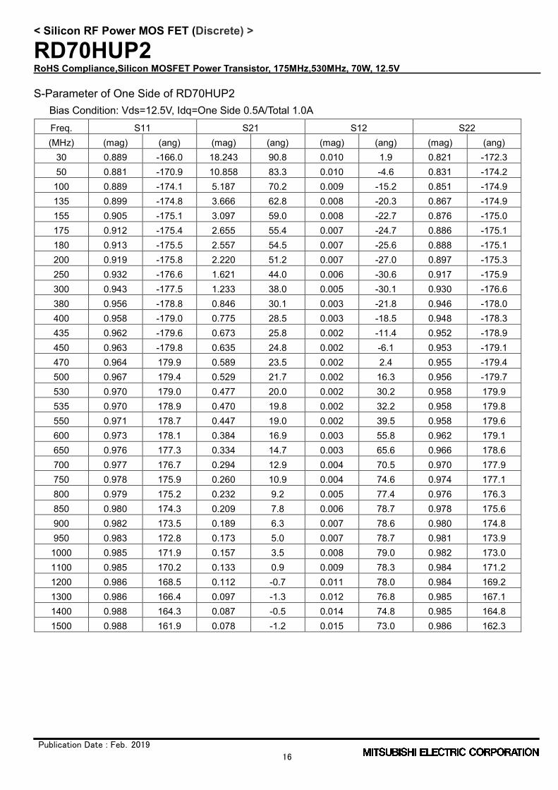
S-Parameter of One Side of RD70HUP2 Bias Condition: Vds=12.5V, Idq=One Side 0.5A/Total 1.0A Freq. S11 S21 S12 S22 (MHz) (mag) (ang) (mag) (ang) (mag) (ang) (mag) (ang)
30 0.889 -166.0 18.243 90.8 0.010 1.9 0.821 -172.3 50 0.881 -170.9 10.858 83.3 0.010 -4.6 0.831 -174.2 100 0.889 -174.1 5.187 70.2 0.009 -15.2 0.851 -174.9 135 0.899 -174.8 3.666 62.8 0.008 -20.3 0.867 -174.9 155 0.905 -175.1 3.097 59.0 0.008 -22.7 0.876 -175.0 175 0.912 -175.4 2.655 55.4 0.007 -24.7 0.886 -175.1 180 0.913 -175.5 2.557 54.5 0.007 -25.6 0.888 -175.1 200 0.919 -175.8 2.220 51.2 0.007 -27.0 0.897 -175.3 250 0.932 -176.6 1.621 44.0 0.006 -30.6 0.917 -175.9 300 0.943 -177.5 1.233 38.0 0.005 -30.1 0.930 -176.6 380 0.956 -178.8 0.846 30.1 0.003 -21.8 0.946 -178.0 400 0.958 -179.0 0.775 28.5 0.003 -18.5 0.948 -178.3 435 0.962 -179.6 0.673 25.8 0.002 -11.4 0.952 -178.9 450 0.963 -179.8 0.635 24.8 0.002 -6.1 0.953 -179.1 470 0.964 179.9 0.589 23.5 0.002 2.4 0.955 -179.4 500 0.967 179.4 0.529 21.7 0.002 16.3 0.956 -179.7 530 0.970 179.0 0.477 20.0 0.002 30.2 0.958 179.9 535 0.970 178.9 0.470 19.8 0.002 32.2 0.958 179.8 550 0.971 178.7 0.447 19.0 0.002 39.5 0.958 179.6 600 0.973 178.1 0.384 16.9 0.003 55.8 0.962 179.1 650 0.976 177.3 0.334 14.7 0.003 65.6 0.966 178.6 700 0.977 176.7 0.294 12.9 0.004 70.5 0.970 177.9 750 0.978 175.9 0.260 10.9 0.004 74.6 0.974 177.1 800 0.979 175.2 0.232 9.2 0.005 77.4 0.976 176.3 850 0.980 174.3 0.209 7.8 0.006 78.7 0.978 175.6 900 0.982 173.5 0.189 6.3 0.007 78.6 0.980 174.8 950 0.983 172.8 0.173 5.0 0.007 78.7 0.981 173.9 1000 0.985 171.9 0.157 3.5 0.008 79.0 0.982 173.0 1100 0.985 170.2 0.133 0.9 0.009 78.3 0.984 171.2 1200 0.986 168.5 0.112 -0.7 0.011 78.0 0.984 169.2 1300 0.986 166.4 0.097 -1.3 0.012 76.8 0.985 167.1 1400 0.988 164.3 0.087 -0.5 0.014 74.8 0.985 164.8 1500 0.988 161.9 0.078 -1.2 0.015 73.0 0.986 162.3
< Silicon RF Power MOS FET (Discrete) >
RD70HUP2 RoHS Compliance,Silicon MOSFET Power Transistor, 175MHz,530MHz, 70W, 12.5V
Publication Date : Feb.2019
17
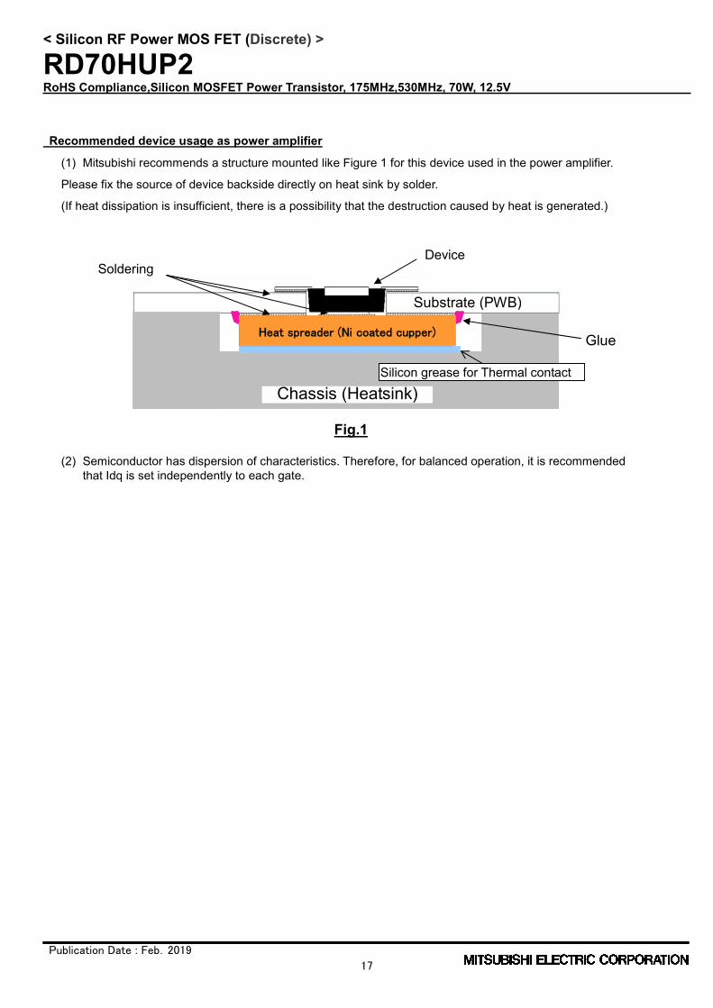
Recommended device usage as power amplifier
(1) Mitsubishi recommends a structure mounted like Figure 1 for this device used in the power amplifier.
Please fix the source of device backside directly on heat sink by solder.
(If heat dissipation is insufficient, there is a possibility that the destruction caused by heat is generated.)
(2) Semiconductor has dispersion of characteristics. Therefore, for balanced operation, it is recommended that Idq is set independently to each gate.
Substrate (PWB)
Heat spreader (Ni coated cupper)
Silicon grease for Thermal contact
Chassis (Heatsink)
Fig.1
Device Soldering
Glue
< Silicon RF Power MOS FET (Discrete) >
RD70HUP2 RoHS Compliance,Silicon MOSFET Power Transistor, 175MHz,530MHz, 70W, 12.5V
Publication Date : Feb.2019
18
ATTENTION: 1.High Temperature ; This product might have a heat generation while operation,Please take notice that have
a possibility to receive a burn to touch the operating product directly or touch the product until cold after switch off. At the near the product,do not place the combustible material that have possibilities to arise the fire.
2.Generation of High Frequency Power ; This product generate a high frequency power. Please take noticethat do not leakage the unnecessary electric wave and use this products without cause damage for human and property per normal operation.
3.Before use; Before use the product,Please design the equipment in consideration of the risk for human and electric wave obstacle for equipment.
PRECAUTIONS FOR THE USE OF MITSUBISHI SILICON RF POWER DEVICES:
1. The specifications of mention are not guarantee values in this data sheet. Please confirm additional details regarding operation of these products from the formal specification sheet. For copies of the formal specification sheets, please contact one of our sales offices.
2.RA series products (RF power amplifier modules) and RD series products (RF power transistors) are
designed for consumer mobile communication terminals and were not specifically designed for use in other applications. In particular, while these products are highly reliable for their designed purpose, they are not manufactured under a quality assurance testing protocol that is sufficient to guarantee the level of reliability typically deemed necessary for critical communications elements and In the application, which is base station applications and fixed station applications that operate with long term continuous transmission and a higher on-off frequency during transmitting, please consider the derating, the redundancy system, appropriate setting of the maintain period and others as needed. For the reliability report which is described about predicted operating life time of Mitsubishi Silicon RF Products , please contact Mitsubishi Electric Corporation or an authorized Mitsubishi Semiconductor product distributor.
3. RD series products use MOSFET semiconductor technology. They are sensitive to ESD voltage therefore
appropriate ESD precautions are required.
4. In the case of use in below than recommended frequency, there is possibility to occur that the device is deteriorated or destroyed due to the RF-swing exceed the breakdown voltage.
5. In order to maximize reliability of the equipment, it is better to keep the devices temperature low. It is
recommended to utilize a sufficient sized heat-sink in conjunction with other cooling methods as needed (fan, etc.) to keep the channel temperature for RD series products lower than 120deg/C(in case of Tchmax=150deg/C) ,140deg/C(in case of Tchmax=175deg/C) under standard conditions.
6. Do not use the device at the exceeded the maximum rating condition. In case of plastic molded devices, the
exceeded maximum rating condition may cause blowout, smoldering or catch fire of the molding resin due to extreme short current flow between the drain and the source of the device. These results causes in fire or injury.
7. For specific precautions regarding assembly of these products into the equipment, please refer to the
supplementary items in the specification sheet.
8. Warranty for the product is void if the products protective cap (lid) is removed or if the product is modified in any way from it’s original form.
9. For additional “Safety first” in your circuit design and notes regarding the materials, please refer the last
page of this data sheet.
< Silicon RF Power MOS FET (Discrete) >
RD70HUP2 RoHS Compliance,Silicon MOSFET Power Transistor, 175MHz,530MHz, 70W, 12.5V
Publication Date : Feb.2019
19
© 2019MITSUBISHI ELECTRIC CORPORATION. ALL RIGHTS RESERVED.
Keep safety first in your circuit designs!
Mitsubishi Electric Corporation puts the maximum effort into making semiconductor products better and more reliable, but there is always the possibility that trouble may occur with them. Trouble with semiconductors may lead to personal injury, fire or property damage. Remember to give due consideration to safety when making your circuit designs, with appropriate measures such as (i) placement of substitutive, auxiliary circuits, (ii) use of non-flammable material or (iii) prevention against any malfunction or mishap.
Notes regarding these materials
•These materials are intended as a reference to assist our customers in the selection of the Mitsubishi semiconductor product best suited to the customer’s application; they do not convey any license under any intellectual property rights, or any other rights, belonging to Mitsubishi Electric Corporation or a third party.
•Mitsubishi Electric Corporation assumes no responsibility for any damage, or infringement of any third-party’s rights, originating in the use of any product data, diagrams, charts, programs, algorithms, or circuit application examples contained in these materials.
•All information contained in these materials, including product data, diagrams, charts, programs and algorithms represents information on products at the time of publication of these materials, and are subject to change by Mitsubishi Electric Corporation without notice due to product improvements or other reasons. It is therefore recommended that customers contact Mitsubishi Electric Corporation or an authorized Mitsubishi Semiconductor product distributor for the latest product information before purchasing a product listed herein. The information described here may contain technical inaccuracies or typographical errors. Mitsubishi Electric Corporation assumes no responsibility for any damage, liability, or other loss rising from these inaccuracies or errors. Please also pay attention to information published by Mitsubishi Electric Corporation by various means, including the Mitsubishi Semiconductor home page (http://www.MitsubishiElectric.com/).
•When using any or all of the information contained in these materials, including product data, diagrams, charts, programs, and algorithms, please be sure to evaluate all information as a total system before making a final decision on the applicability of the information and products. Mitsubishi Electric Corporation assumes no responsibility for any damage, liability or other loss resulting from the information contained herein.
•Mitsubishi Electric Corporation semiconductors are not designed or manufactured for use in a device or system that is used under circumstances in which human life is potentially at stake. Please contact Mitsubishi Electric Corporation or an authorized Mitsubishi Semiconductor product distributor when considering the use of a product contained herein for any specific purposes, such as apparatus or systems for transportation, vehicular, medical, aerospace, nuclear, or undersea repeater use.
•The prior written approval of Mitsubishi Electric Corporation is necessary to reprint or reproduce in whole or in part these materials.
•If these products or technologies are subject to the Japanese export control restrictions, they must be exported under a license from the Japanese government and cannot be imported into a country other than the approved destination. Any diversion or re-export contrary to the export control laws and regulations of Japan and/or the country of destination is prohibited.
•Please contact Mitsubishi Electric Corporation or an authorized Mitsubishi Semiconductor product distributor for further details on these materials or the products contained therein.
10. Please avoid use in the place where water or organic solvents can adhere directly to the product and the environments with the possibility of caustic gas, dust, salinity, etc. Reliability could be markedly decreased and also there is a possibility failures could result causing a serious accident. Likewise, there is a possibility of causing a serious accident if used in an explosive gas environment. Please allow for adequate safety margin in your designs.
11. Please refer to the additional precautions in the formal specification sheet.