< Silicon RF Power MOS FET (Discrete) > RD35HUF2 · RD35HUF2 RoHS Compliance, Silicon MOSFET Power...
20
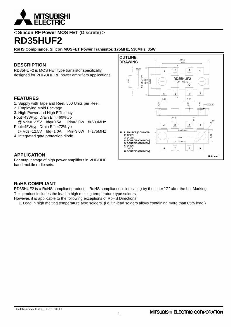
Publication Date : Oct.2011 1 < Silicon RF Power MOS FET (Discrete) > RD35HUF2 RoHS Compliance, Silicon MOSFET Power Transistor, 175MHz, 530MHz, 35W DESCRIPTION RD35HUF2 is MOS FET type transistor specifically designed for VHF/UHF RF power amplifiers applications. FEATURES 1. Supply with Tape and Reel. 500 Units per Reel. 2. Employing Mold Package 3. High Power and High Efficiency Pout=43Wtyp, Drain Effi.=60%typ @ Vds=12.5V Idq=0.5A Pin=3.0W f=530MHz Pout=45Wtyp, Drain Effi.=72%typ @ Vds=12.5V Idq=1.0A Pin=3.0W f=175MHz 4. Integrated gate protection diode APPLICATION For output stage of high power amplifiers in VHF/UHF band mobile radio sets. RoHS COMPLIANT RD35HUF2 is a RoHS compliant product. RoHS compliance is indicating by the letter “G” after the Lot Marking. This product includes the lead in high melting temperature type solders. However, it is applicable to the following exceptions of RoHS Directions. 1. Lead in high melting temperature type solders. (i.e. tin-lead solders alloys containing more than 85% lead.) 24.60 3.63 3.15 18.00 12.69 12.95 6.38 5.56 a a' a-a' SECTION 0.10 3.65 2.40 13.40 5.87 3.10 0.22 0.34 ○ Lot No.-G RD35HUF2 RD35HUF2 Lot No.-G ○ 3.70 0.10 OUTLINE DRAWING 4 1 2 3 5 6 7 8 5 6 7 8 Pin 1. SOURCE (COMMON) 2. OPEN 3. DRAIN 4. SOURCE (COMMON) 5. SOURCE (COMMON) 6. OPEN 7. GATE 8. SOURCE (COMMON) Unit: mm 1 2 3 4
Transcript of < Silicon RF Power MOS FET (Discrete) > RD35HUF2 · RD35HUF2 RoHS Compliance, Silicon MOSFET Power...
Publication Date : Oct.20111
< Silicon RF Power MOS FET (Discrete) >
RD35HUF2RoHS Compliance, Silicon MOSFET Power Transistor, 175MHz, 530MHz, 35W
DESCRIPTIONRD35HUF2 is MOS FET type transistor specificallydesigned for VHF/UHF RF power amplifiers applications.
FEATURES1. Supply with Tape and Reel. 500 Units per Reel.2. Employing Mold Package3. High Power and High EfficiencyPout=43Wtyp, Drain Effi.=60%typ
@ Vds=12.5V Idq=0.5A Pin=3.0W f=530MHzPout=45Wtyp, Drain Effi.=72%typ
@ Vds=12.5V Idq=1.0A Pin=3.0W f=175MHz4. Integrated gate protection diode
APPLICATIONFor output stage of high power amplifiers in VHF/UHFband mobile radio sets.
RoHS COMPLIANTRD35HUF2 is a RoHS compliant product. RoHS compliance is indicating by the letter “G” after the Lot Marking.
This product includes the lead in high melting temperature type solders.However, it is applicable to the following exceptions of RoHS Directions.
1. Lead in high melting temperature type solders. (i.e. tin-lead solders alloys containing more than 85% lead.)
24.60
3.633.15
18.00
12
.69
12
.95
6.3
8
5.5
6
a
a'
a-a
'SE
CT
ION
0.10
3.6
52.40
13.40 5.8
7
3.1
0
0.2
2
0.3
4
○Lot No.-G
RD35HUF2
RD35HUF2
Lot No.-G○
3.70
0.10
OUTLINEDRAWING
41 2 3
5 6 7 8
5678
Pin 1. SOURCE (COMMON)2. OPEN3. DRAIN4. SOURCE (COMMON)5. SOURCE (COMMON)6. OPEN7. GATE8. SOURCE (COMMON)
Unit: mm
1234
< Silicon RF Power MOS FET (Discrete) >
RD35HUF2RoHS Compliance, Silicon MOSFET Power Transistor, 175MHz, 530MHz, 35W
Publication Date : Oct.2011
2
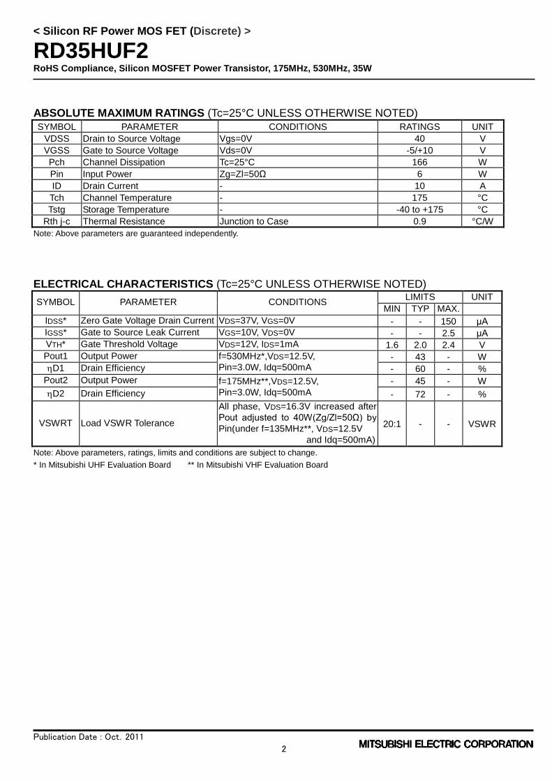
ABSOLUTE MAXIMUM RATINGS (Tc=25°C UNLESS OTHERWISE NOTED)SYMBOL PARAMETER CONDITIONS RATINGS UNIT
VDSS Drain to Source Voltage Vgs=0V 40 V
VGSS Gate to Source Voltage Vds=0V -5/+10 V
Pch Channel Dissipation Tc=25°C 166 W
Pin Input Power Zg=Zl=50Ω 6 W
ID Drain Current - 10 A
Tch Channel Temperature - 175 °C
Tstg Storage Temperature - -40 to +175 °C
Rth j-c Thermal Resistance Junction to Case 0.9 °C/W
Note: Above parameters are guaranteed independently.
ELECTRICAL CHARACTERISTICS (Tc=25°C UNLESS OTHERWISE NOTED)LIMITS UNIT
SYMBOL PARAMETER CONDITIONSMIN TYP MAX.
IDSS* Zero Gate Voltage Drain Current VDS=37V, VGS=0V - - 150 μAIGSS* Gate to Source Leak Current VGS=10V, VDS=0V - - 2.5 μAVTH* Gate Threshold Voltage VDS=12V, IDS=1mA 1.6 2.0 2.4 VPout1 Output Power - 43 - WD1 Drain Efficiency
f=530MHz*,VDS=12.5V,Pin=3.0W, Idq=500mA - 60 - %
Pout2 Output Power - 45 - W
D2 Drain Efficiency
f=175MHz**,VDS=12.5V,Pin=3.0W, Idq=500mA - 72 - %
VSWRT Load VSWR Tolerance
All phase, VDS=16.3V increased afterPout adjusted to 40W(Zg/Zl=50Ω) by Pin(under f=135MHz**, VDS=12.5V
and Idq=500mA)
20:1 - - VSWR
Note: Above parameters, ratings, limits and conditions are subject to change.
* In Mitsubishi UHF Evaluation Board ** In Mitsubishi VHF Evaluation Board
< Silicon RF Power MOS FET (Discrete) >
RD35HUF2RoHS Compliance, Silicon MOSFET Power Transistor, 175MHz, 530MHz, 35W
Publication Date : Oct.2011
3
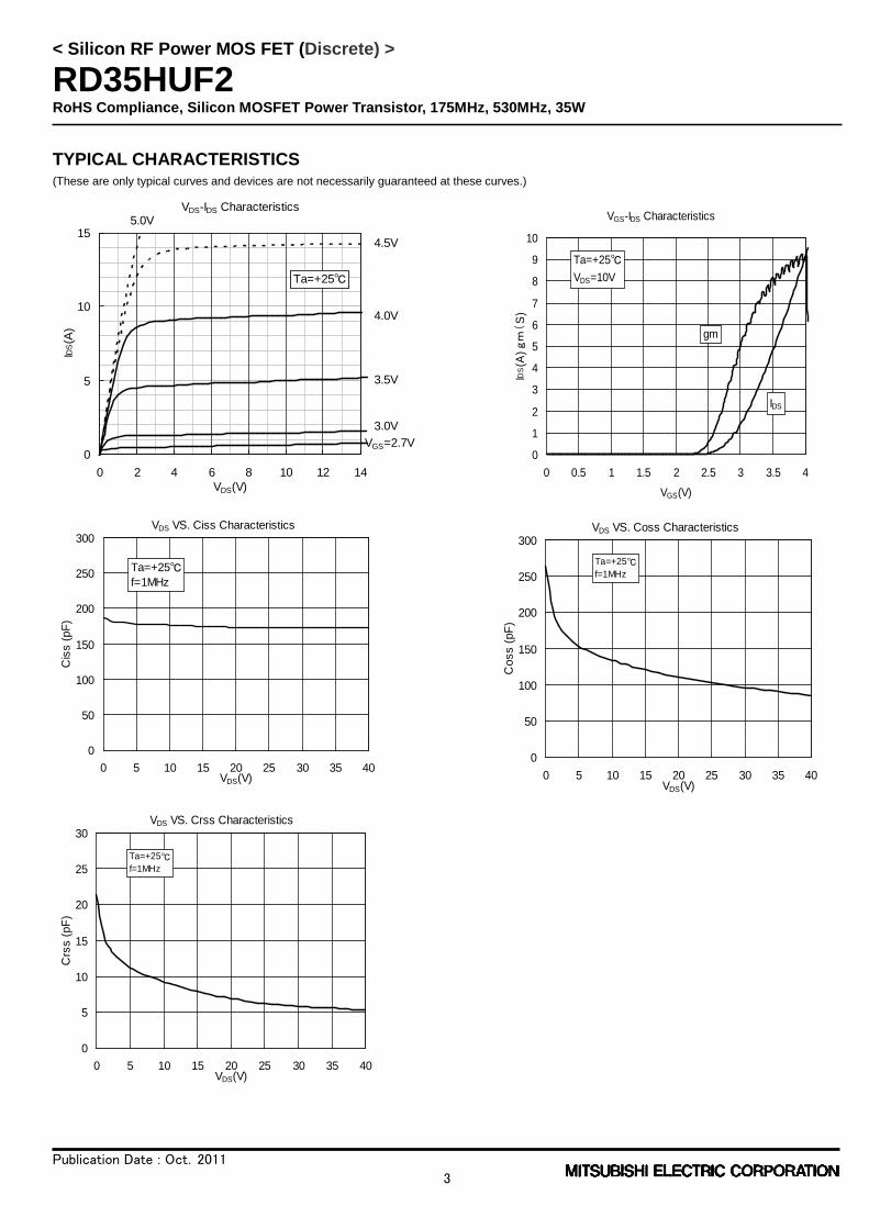
TYPICAL CHARACTERISTICS(These are only typical curves and devices are not necessarily guaranteed at these curves.)
VDS VS. Ciss Characteristics
0
50
100
150
200
250
300
0 5 10 15 20 25 30 35 40VDS(V)
Cis
s(p
F)
Ta=+25℃f=1MHz
VDS VS. Coss Characteristics
0
50
100
150
200
250
300
0 5 10 15 20 25 30 35 40VDS(V)
Co
ss
(pF
)
Ta=+25℃f=1MHz
VDS VS. Crss Characteristics
0
5
10
15
20
25
30
0 5 10 15 20 25 30 35 40VDS(V)
Crs
s(p
F)
Ta=+25℃f=1MHz
VDS-IDS Characteristics
0
5
10
15
0 2 4 6 8 10 12 14VDS(V)
IDS(A
)
3.0V
3.5V
4.0V
4.5V
5.0V
Ta=+25℃
VGS=2.7V
VGS-IDS Characteristics
0
1
2
3
4
5
6
7
8
9
10
0 0.5 1 1.5 2 2.5 3 3.5 4
VGS(V)
IDS(A
)gm
(S
)
gm
IDS
Ta=+25℃
VDS=10V
< Silicon RF Power MOS FET (Discrete) >
RD35HUF2RoHS Compliance, Silicon MOSFET Power Transistor, 175MHz, 530MHz, 35W
Publication Date : Oct.2011
4
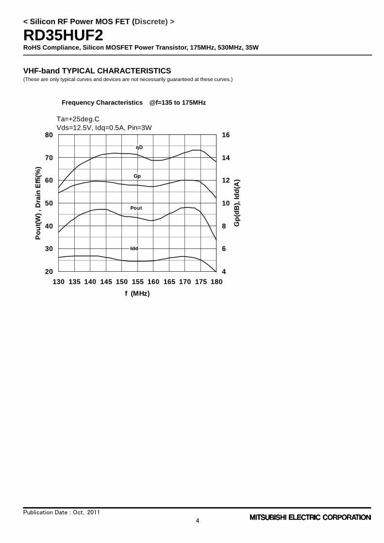
VHF-band TYPICAL CHARACTERISTICS(These are only typical curves and devices are not necessarily guaranteed at these curves.)
Frequency Characteristics @f=135 to 175MHz
20
30
40
50
60
70
80
130 135 140 145 150 155 160 165 170 175 180
f (MHz)
Po
ut(
W)
,D
rain
Eff
i(%
)
4
6
8
10
12
14
16
Gp
(dB
),Id
d(A
)
Pout
ηD
Gp
Ta=+25deg.C
Vds=12.5V, Idq=0.5A, Pin=3W
Idd
< Silicon RF Power MOS FET (Discrete) >
RD35HUF2RoHS Compliance, Silicon MOSFET Power Transistor, 175MHz, 530MHz, 35W
Publication Date : Oct.2011
5
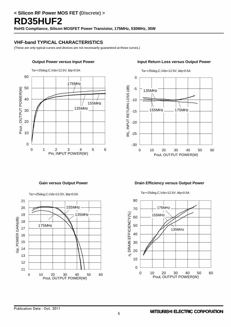
VHF-band TYPICAL CHARACTERISTICS(These are only typical curves and devices are not necessarily guaranteed at these curves.)
Output Power versus Input Power Input Return Loss versus Output Power
Gain versus Output Power Drain Efficiency versus Output Power
0
10
20
30
40
50
60
0 1 2 3 4 5 6Pin, INPUT POWER(W)
Po
ut,O
UT
PU
TP
OW
ER
(W)
Ta=+25deg.C,Vds=12.5V, Idq=0.5A
175MHz
135MHz
155MHz
-30
-25
-20
-15
-10
-5
0
0 10 20 30 40 50 60
Pout, OUTPUT POWER(W)
IRL,
INP
UT
RE
TU
RN
LO
SS
(dB
)
Ta=+25deg.C,Vds=12.5V, Idq=0.5A
135MHz
175MHz155MHz
0
10
20
30
40
50
60
70
80
0 10 20 30 40 50 60Pout, OUTPUT POWER(W)
η, D
RA
IN E
FF
ICIE
NC
Y(%
)
Ta=+25deg.C,Vds=12.5V, Idq=0.5A
135MHz
175MHz
155MHz
11
12
13
14
15
16
17
18
19
20
21
0 10 20 30 40 50 60Pout, OUTPUT POWER(W)
Gp,P
OW
ER
GA
IN(d
B)
Ta=+25deg.C,Vds=12.5V, Idq=0.5A
155MHz
135MHz
175MHz
< Silicon RF Power MOS FET (Discrete) >
RD35HUF2RoHS Compliance, Silicon MOSFET Power Transistor, 175MHz, 530MHz, 35W
Publication Date : Oct.2011
6
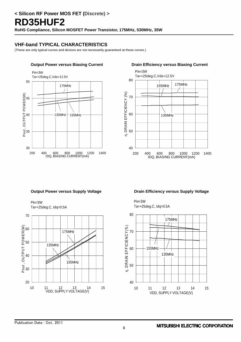
VHF-band TYPICAL CHARACTERISTICS(These are only typical curves and devices are not necessarily guaranteed at these curves.)
Output Power versus Biasing Current Drain Efficiency versus Biasing Current
Output Power versus Supply Voltage Drain Efficiency versus Supply Voltage
30
35
40
45
50
200 400 600 800 1000 1200 1400IDQ, BIASING CURRENT(mA)
Po
ut
,O
UT
PU
TP
OW
ER
(W)
Pin=3W
Ta=+25deg.C,Vds=12.5V
175MHz
135MHz 155MHz
40
50
60
70
80
200 400 600 800 1000 1200 1400IDQ, BIASING CURRENT(mA)
η,D
RA
INE
FF
ICIE
NC
Y(%
)
Pin=3W
Ta=+25deg.C,Vds=12.5V
135MHz
175MHz155MHz
Pin=3W
Ta=+25deg.C, Idq=0.5A
20
30
40
50
60
70
10 11 12 13 14 15VDD, SUPPLY VOLTAGE(V)
Po
ut
,O
UT
PU
TP
OW
ER
(W)
175MHz
155MHz
135MHz
Pin=3W
Ta=+25deg.C, Idq=0.5A
40
50
60
70
80
10 11 12 13 14 15VDD, SUPPLY VOLTAGE(V)
η,
DR
AIN
EF
FIC
IEN
CY
(%)
175MHz
155MHz
135MHz
< Silicon RF Power MOS FET (Discrete) >
RD35HUF2RoHS Compliance, Silicon MOSFET Power Transistor, 175MHz, 530MHz, 35W
Publication Date : Oct.2011
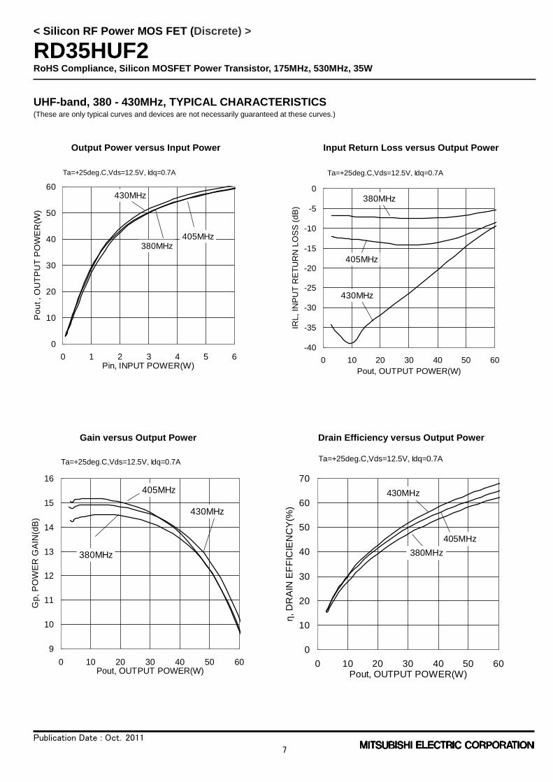
7
UHF-band, 380 - 430MHz, TYPICAL CHARACTERISTICS(These are only typical curves and devices are not necessarily guaranteed at these curves.)
Output Power versus Input Power Input Return Loss versus Output Power
Gain versus Output Power Drain Efficiency versus Output Power
0
10
20
30
40
50
60
70
0 10 20 30 40 50 60Pout, OUTPUT POWER(W)
η,D
RA
INE
FF
ICIE
NC
Y(%
)
Ta=+25deg.C,Vds=12.5V, Idq=0.7A
380MHz
430MHz
405MHz
9
10
11
12
13
14
15
16
0 10 20 30 40 50 60Pout, OUTPUT POWER(W)
Gp
,P
OW
ER
GA
IN(d
B)
Ta=+25deg.C,Vds=12.5V, Idq=0.7A
380MHz
430MHz
405MHz
0
10
20
30
40
50
60
0 1 2 3 4 5 6Pin, INPUT POWER(W)
Po
ut,O
UT
PU
TP
OW
ER
(W)
Ta=+25deg.C,Vds=12.5V, Idq=0.7A
380MHz405MHz
430MHz
-40
-35
-30
-25
-20
-15
-10
-5
0
0 10 20 30 40 50 60
Pout, OUTPUT POWER(W)
IRL,
INP
UT
RE
TU
RN
LO
SS
(dB
)
Ta=+25deg.C,Vds=12.5V, Idq=0.7A
380MHz
430MHz
405MHz
< Silicon RF Power MOS FET (Discrete) >
RD35HUF2RoHS Compliance, Silicon MOSFET Power Transistor, 175MHz, 530MHz, 35W
Publication Date : Oct.2011
8
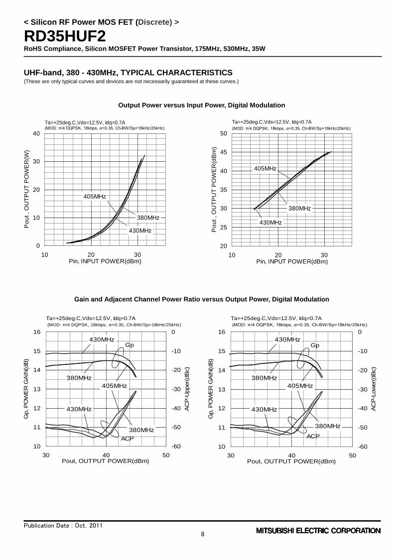
UHF-band, 380 - 430MHz, TYPICAL CHARACTERISTICS(These are only typical curves and devices are not necessarily guaranteed at these curves.)
Output Power versus Input Power, Digital Modulation
Gain and Adjacent Channel Power Ratio versus Output Power, Digital Modulation
10
11
12
13
14
15
16
30 40 50Pout, OUTPUT POWER(dBm)
Gp,P
OW
ER
GA
IN(d
B)
-60
-50
-40
-30
-20
-10
0
AC
P-L
ow
er(
dB
c)
Ta=+25deg.C,Vds=12.5V, Idq=0.7A(MOD: π/4 DQPSK, 18kbps, α=0.35, Ch-BW/Sp=18kHz/25kHz)
405MHz
430MHz
380MHz
380MHz
430MHz
Gp
ACP
10
11
12
13
14
15
16
30 40 50Pout, OUTPUT POWER(dBm)
Gp,P
OW
ER
GA
IN(d
B)
-60
-50
-40
-30
-20
-10
0
AC
P-U
pper(
dB
c)
Ta=+25deg.C,Vds=12.5V, Idq=0.7A(MOD: π/4 DQPSK, 18kbps, α=0.35, Ch-BW/Sp=18kHz/25kHz)
405MHz
430MHz
380MHz
380MHz
430MHz
Gp
ACP
20
25
30
35
40
45
50
10 20 30Pin, INPUT POWER(dBm)
Po
ut,O
UT
PU
TP
OW
ER
(dB
m)
Ta=+25deg.C,Vds=12.5V, Idq=0.7A(MOD: π/4 DQPSK, 18kbps, α=0.35, Ch-BW/Sp=18kHz/25kHz)
405MHz
430MHz
380MHz
0
10
20
30
40
10 20 30Pin, INPUT POWER(dBm)
Po
ut,O
UT
PU
TP
OW
ER
(W)
Ta=+25deg.C,Vds=12.5V, Idq=0.7A(MOD: π/4 DQPSK, 18kbps, α=0.35, Ch-BW/Sp=18kHz/25kHz)
380MHz
430MHz
405MHz
< Silicon RF Power MOS FET (Discrete) >
RD35HUF2RoHS Compliance, Silicon MOSFET Power Transistor, 175MHz, 530MHz, 35W
Publication Date : Oct.2011
9
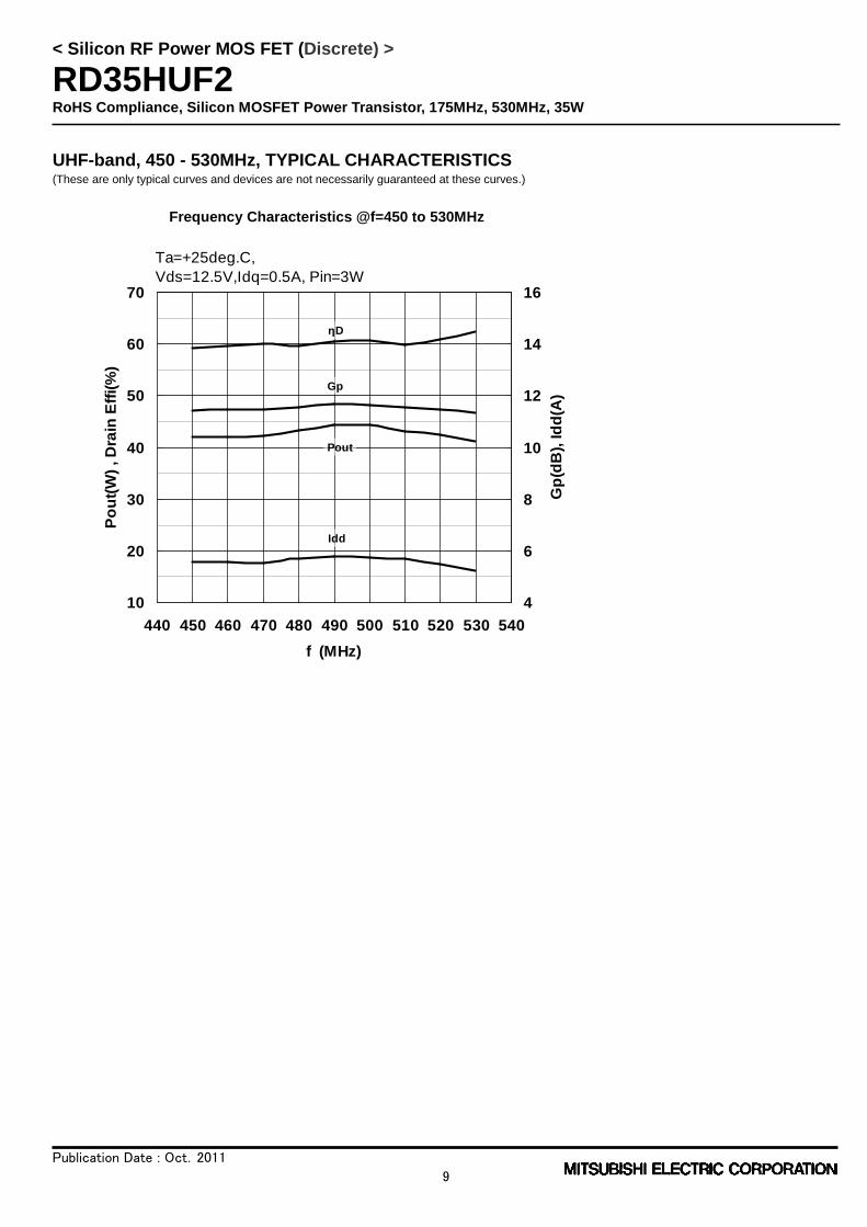
UHF-band, 450 - 530MHz, TYPICAL CHARACTERISTICS(These are only typical curves and devices are not necessarily guaranteed at these curves.)
Frequency Characteristics @f=450 to 530MHz
10
20
30
40
50
60
70
440 450 460 470 480 490 500 510 520 530 540
f (MHz)
Po
ut(
W)
,D
rain
Eff
i(%
)
4
6
8
10
12
14
16
Gp
(dB
),Id
d(A
)
Pout
ηD
Gp
Idd
Ta=+25deg.C,
Vds=12.5V,Idq=0.5A, Pin=3W
< Silicon RF Power MOS FET (Discrete) >
RD35HUF2RoHS Compliance, Silicon MOSFET Power Transistor, 175MHz, 530MHz, 35W
Publication Date : Oct.2011
10
UHF-band, 450 - 530MHz, TYPICAL CHARACTERISTICS(These are only typical curves and devices are not necessarily guaranteed at these curves.)
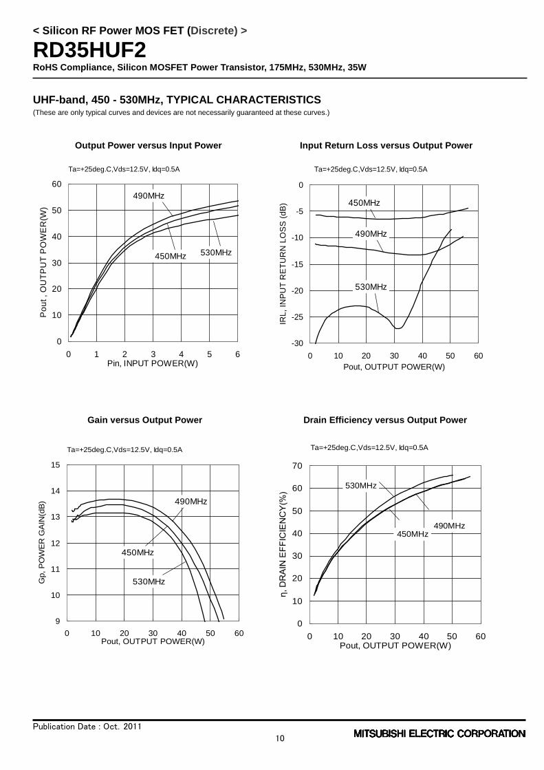
Output Power versus Input Power Input Return Loss versus Output Power
Gain versus Output Power Drain Efficiency versus Output Power
9
10
11
12
13
14
15
0 10 20 30 40 50 60Pout, OUTPUT POWER(W)
Gp,P
OW
ER
GA
IN(d
B)
Ta=+25deg.C,Vds=12.5V, Idq=0.5A
450MHz
530MHz
490MHz
-30
-25
-20
-15
-10
-5
0
0 10 20 30 40 50 60
Pout, OUTPUT POWER(W)
IRL
,IN
PU
TR
ET
UR
NL
OS
S(d
B)
Ta=+25deg.C,Vds=12.5V, Idq=0.5A
450MHz
530MHz
490MHz
0
10
20
30
40
50
60
70
0 10 20 30 40 50 60Pout, OUTPUT POWER(W)
η, D
RA
IN E
FF
ICIE
NC
Y(%
)
Ta=+25deg.C,Vds=12.5V, Idq=0.5A
450MHz
530MHz
490MHz
0
10
20
30
40
50
60
0 1 2 3 4 5 6Pin, INPUT POWER(W)
Po
ut,O
UT
PU
TP
OW
ER
(W)
Ta=+25deg.C,Vds=12.5V, Idq=0.5A
450MHz 530MHz
490MHz
< Silicon RF Power MOS FET (Discrete) >
RD35HUF2RoHS Compliance, Silicon MOSFET Power Transistor, 175MHz, 530MHz, 35W
Publication Date : Oct.2011
11
UHF-band, 450 - 530MHz, TYPICAL CHARACTERISTICS(These are only typical curves and devices are not necessarily guaranteed at these curves.)
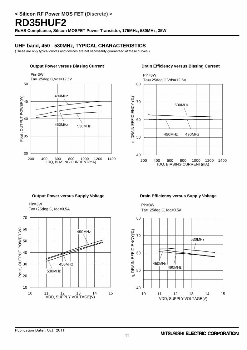
Output Power versus Biasing Current Drain Efficiency versus Biasing Current
Output Power versus Supply Voltage Drain Efficiency versus Supply Voltage
Pin=3W
Ta=+25deg.C, Idq=0.5A
40
50
60
70
80
10 11 12 13 14 15VDD, SUPPLY VOLTAGE(V)
η,
DR
AIN
EF
FIC
IEN
CY
(%)
530MHz
490MHz450MHz
Pin=3W
Ta=+25deg.C, Idq=0.5A
10
20
30
40
50
60
70
10 11 12 13 14 15VDD, SUPPLY VOLTAGE(V)
Po
ut
,O
UT
PU
TP
OW
ER
(W)
490MHz
450MHz
530MHz
40
50
60
70
80
200 400 600 800 1000 1200 1400IDQ, BIASING CURRENT(mA)
η, D
RA
IN E
FF
ICIE
NC
Y (
%)
Pin=3W
Ta=+25deg.C,Vds=12.5V
450MHz
530MHz
490MHz
30
35
40
45
50
200 400 600 800 1000 1200 1400IDQ, BIASING CURRENT(mA)
Po
ut,O
UT
PU
TP
OW
ER
(W)
Pin=3W
Ta=+25deg.C,Vds=12.5V
490MHz
450MHz 530MHz
< Silicon RF Power MOS FET (Discrete) >
RD35HUF2RoHS Compliance, Silicon MOSFET Power Transistor, 175MHz, 530MHz, 35W
Publication Date : Oct.2011
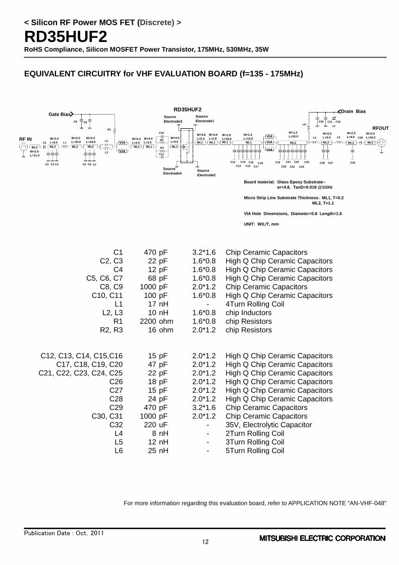
12
EQUIVALENT CIRCUITRY for VHF EVALUATION BOARD (f=135 - 175MHz)
For more information regarding this evaluation board, refer to APPLICATION NOTE “AN-VHF-048”
VIA
VIA
VIA
VIA
VIA
Drain Bias
ML2 ML2 ML2 ML2 ML1 ML1 ML1
ML1 ML1 ML1 ML2 ML2 ML2 ML2ML1
W=2.0
L=4.0
W=2.0
L=11.0
W=2.0
L=10.0
W=2.0
L=18.0W=2.2
L=3.0
W=4.0
L=3.0
W=4.0
L=5.0
W=4.6
L=5.3
W=3.6
L=2.9W=1.8
L=15.0
W=1.2
L=20.0W=2.0
L=5.0
W=2.0
L=9.0W=2.0
L=16.0W=1.2
L=15.0
L1L2
L3
L4 L5
L6
C2 C3 C4 C5 C6 C7
C1
C9 C8
C11
C10
C12
C13
C14
C15
C16
C17
C18 C19
C20
C21
C22
C23
C24
C25 C26 C27 C28
C29
C30 C31 C32
R2
R1
RF IN
RFOUT
RD35HUF2Gate Bias
Source
Electrode3
Source
Electrode1
SourceElectrode2
SourceElectrode4
Board material: Glass Epoxy Substrate--er=4.8, TanD=0.018 @1GHz
Micro Strip Line Substrate Thickness: ML1, T=0.2
ML2, T=1.1
VIA Hole Dimensions, Diameter=0.8 Length=1.6
UNIT: W/L/T, mm
R3
C1 470 pF 3.2*1.6 Chip Ceramic CapacitorsC2, C3 22 pF 1.6*0.8 High Q Chip Ceramic Capacitors
C4 12 pF 1.6*0.8 High Q Chip Ceramic CapacitorsC5, C6, C7 68 pF 1.6*0.8 High Q Chip Ceramic Capacitors
C8, C9 1000 pF 2.0*1.2 Chip Ceramic CapacitorsC10, C11 100 pF 1.6*0.8 High Q Chip Ceramic Capacitors
L1 17 nH - 4Turn Rolling CoilL2, L3 10 nH 1.6*0.8 chip Inductors
R1 2200 ohm 1.6*0.8 chip ResistorsR2, R3 16 ohm 2.0*1.2 chip Resistors
C12, C13, C14, C15,C16 15 pF 2.0*1.2 High Q Chip Ceramic CapacitorsC17, C18, C19, C20 47 pF 2.0*1.2 High Q Chip Ceramic Capacitors
C21, C22, C23, C24, C25 22 pF 2.0*1.2 High Q Chip Ceramic CapacitorsC26 18 pF 2.0*1.2 High Q Chip Ceramic CapacitorsC27 15 pF 2.0*1.2 High Q Chip Ceramic CapacitorsC28 24 pF 2.0*1.2 High Q Chip Ceramic CapacitorsC29 470 pF 3.2*1.6 Chip Ceramic Capacitors
C30, C31 1000 pF 2.0*1.2 Chip Ceramic CapacitorsC32 220 uF - 35V, Electrolytic Capacitor
L4 8 nH - 2Turn Rolling CoilL5 12 nH - 3Turn Rolling CoilL6 25 nH - 5Turn Rolling Coil
< Silicon RF Power MOS FET (Discrete) >
RD35HUF2RoHS Compliance, Silicon MOSFET Power Transistor, 175MHz, 530MHz, 35W
Publication Date : Oct.2011
13
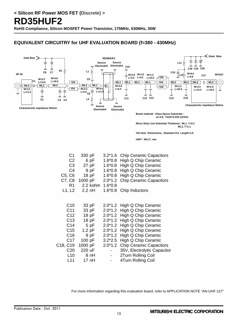
EQUIVALENT CIRCUITRY for UHF EVALUATION BOARD (f=380 - 430MHz)
For more information regarding this evaluation board, refer to APPLICATION NOTE “AN-UHF-127”
Board material: Glass Epoxy Substrate--
er=4.8, TanD=0.018 @1GHz
Micro Strip Line Substrate Thickness: ML1, T=0.2
ML2, T=1.1
VIA Hole Dimensions, Diameter=0.8 Length=1.6
UNIT: W/L/T, mm
RD35HUF2
C1
C2
ML2
RF IN
ML1 ML1ML1 ML1 ML1 ML1 VIAVIA ML2 ML2 ML2 ML2
VIAVIA
VIA
C3 L2
C5
C7C8R1
L10
C10
C11 C12 C13 C14
C15
C18 C19
W=4.0
L=11.5W=2.2
L=3.0
W=0.8
L=18.0W=2.0
L=14.0
W=2.0
L=11.0
W=4.6
L=5.3
W=3.6
L=2.9
W=1.8
L=4.5W=1.2
L=15.0
W=1.2
L=20.0
W=6.6
L=4.8
W=2.0
L=14.0
W=2.0
L=16.0
Characteristic impidance 50ohmCharacteristic impidance 50ohm
C20
RFOUT
Drain BiasGate Bias
Source
Electrode1
Source
Electrode2
Source
Electrode4
Source
Electrode3
C4
L1
L11
C16
C17
C6
ML2ML2
C1 330 pF 3.2*1.6 Chip Ceramic CapacitorsC2 6 pF 1.6*0.8 High Q Chip CeramicC3 27 pF 1.6*0.8 High Q Chip CeramicC4 9 pF 1.6*0.8 High Q Chip Ceramic
C5, C6 18 pF 1.6*0.8 High Q Chip CeramicC7, C8 1000 pF 2.0*1.2 Chip Ceramic Capacitors
R1 2.2 kohm 1.6*0.8L1, L2 2.2 nH 1.6*0.8 Chip Inductors
C10 33 pF 2.0*1.2 High Q Chip CeramicC11 33 pF 2.0*1.2 High Q Chip CeramicC12 18 pF 2.0*1.2 High Q Chip CeramicC13 18 pF 2.0*1.2 High Q Chip CeramicC14 5 pF 2.0*1.2 High Q Chip CeramicC15 1.2 pF 2.0*1.2 High Q Chip CeramicC16 9 pF 2.0*1.2 High Q Chip CeramicC17 100 pF 3.2*2.5 High Q Chip Ceramic
C18, C19 1000 pF 2.0*1.2 Chip Ceramic CapacitorsC20 220 uF - 35V, Electrolytic CapacitorL10 8 nH - 2Turn Rolling CoilL11 17 nH - 4Turn Rolling Coil
< Silicon RF Power MOS FET (Discrete) >
RD35HUF2RoHS Compliance, Silicon MOSFET Power Transistor, 175MHz, 530MHz, 35W
Publication Date : Oct.2011
14
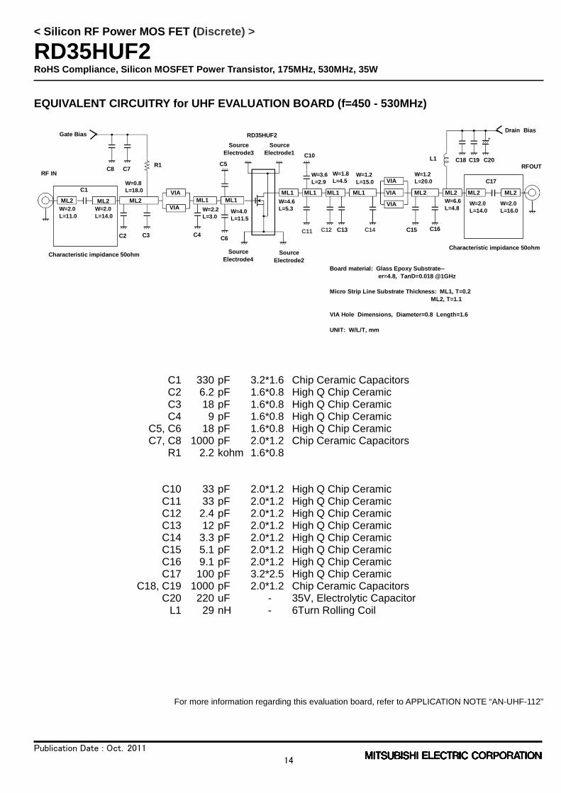
EQUIVALENT CIRCUITRY for UHF EVALUATION BOARD (f=450 - 530MHz)
For more information regarding this evaluation board, refer to APPLICATION NOTE “AN-UHF-112”
ML2
Board material: Glass Epoxy Substrate--
er=4.8, TanD=0.018 @1GHz
Micro Strip Line Substrate Thickness: ML1, T=0.2
ML2, T=1.1
VIA Hole Dimensions, Diameter=0.8 Length=1.6
UNIT: W/L/T, mm
RD35HUF2
C1
C2
ML2
RF IN
ML2 ML1 ML1
ML1 ML1 ML1 ML1 VIAVIA ML2 ML2 ML2 ML2
VIAVIA
VIA
C3 C4C6
C5C7C8
R1L1
C10
C11 C12 C13 C14 C15
C18 C19
W=4.0
L=11.5
W=2.2
L=3.0
W=0.8
L=18.0
W=2.0
L=14.0
W=2.0
L=11.0
W=4.6
L=5.3
W=3.6
L=2.9
W=1.8
L=4.5W=1.2
L=15.0
W=1.2
L=20.0
W=6.6
L=4.8W=2.0
L=14.0
W=2.0
L=16.0
Characteristic impidance 50ohmCharacteristic impidance 50ohm
C20RFOUT
Drain BiasGate Bias
Source
Electrode1
Source
Electrode2
Source
Electrode4
Source
Electrode3
C16
C17
C1 330 pF 3.2*1.6 Chip Ceramic CapacitorsC2 6.2 pF 1.6*0.8 High Q Chip CeramicC3 18 pF 1.6*0.8 High Q Chip CeramicC4 9 pF 1.6*0.8 High Q Chip Ceramic
C5, C6 18 pF 1.6*0.8 High Q Chip CeramicC7, C8 1000 pF 2.0*1.2 Chip Ceramic Capacitors
R1 2.2 kohm 1.6*0.8
C10 33 pF 2.0*1.2 High Q Chip CeramicC11 33 pF 2.0*1.2 High Q Chip CeramicC12 2.4 pF 2.0*1.2 High Q Chip CeramicC13 12 pF 2.0*1.2 High Q Chip CeramicC14 3.3 pF 2.0*1.2 High Q Chip CeramicC15 5.1 pF 2.0*1.2 High Q Chip CeramicC16 9.1 pF 2.0*1.2 High Q Chip CeramicC17 100 pF 3.2*2.5 High Q Chip Ceramic
C18, C19 1000 pF 2.0*1.2 Chip Ceramic CapacitorsC20 220 uF - 35V, Electrolytic Capacitor
L1 29 nH - 6Turn Rolling Coil
< Silicon RF Power MOS FET (Discrete) >
RD35HUF2RoHS Compliance, Silicon MOSFET Power Transistor, 175MHz, 530MHz, 35W
Publication Date : Oct.2011
15
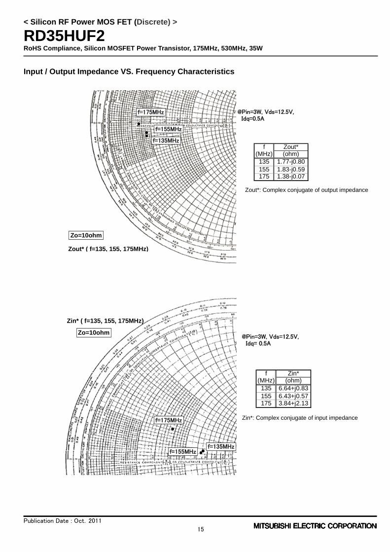
Input / Output Impedance VS. Frequency Characteristics
Zout*: Complex conjugate of output impedance
Zin*: Complex conjugate of input impedance
f Zout*(MHz) (ohm)135 1.77-j0.80155 1.83-j0.59175 1.38-j0.07
f=175MHz
f=155MHz
f=135MHz
Zout* ( f=135, 155, 175MHz)
Zo=10ohm
@Pin=3W, Vds=12.5V,Idq=0.5A
f Zin*(MHz) (ohm)135 6.64+j0.83155 6.43+j0.57175 3.84+j2.13
f=135MHzf=155MHz
f=175MHz
Zin* ( f=135, 155, 175MHz)
Zo=10ohm@Pin=3W, Vds=12.5V,Idq= 0.5A
< Silicon RF Power MOS FET (Discrete) >
RD35HUF2RoHS Compliance, Silicon MOSFET Power Transistor, 175MHz, 530MHz, 35W
Publication Date : Oct.2011
16
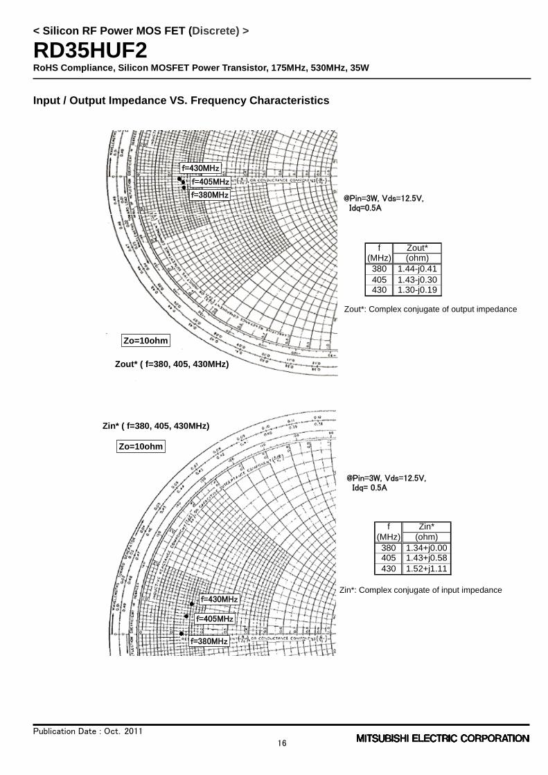
Input / Output Impedance VS. Frequency Characteristics
Zout*: Complex conjugate of output impedance
Zin*: Complex conjugate of input impedance
f Zout*(MHz) (ohm)380 1.44-j0.41405 1.43-j0.30430 1.30-j0.19
f=380MHz
f=405MHz
f=430MHz
Zout* ( f=380, 405, 430MHz)
Zo=10ohm
@Pin=3W, Vds=12.5V,Idq=0.5A
f Zin*(MHz) (ohm)380 1.34+j0.00405 1.43+j0.58430 1.52+j1.11
f=380MHz
f=405MHz
f=430MHz
Zin* ( f=380, 405, 430MHz)
Zo=10ohm
@Pin=3W, Vds=12.5V,Idq= 0.5A
< Silicon RF Power MOS FET (Discrete) >
RD35HUF2RoHS Compliance, Silicon MOSFET Power Transistor, 175MHz, 530MHz, 35W
Publication Date : Oct.2011
17
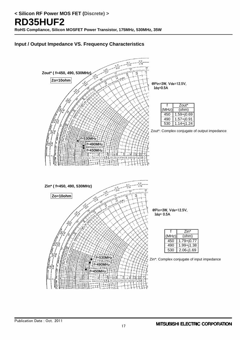
Input / Output Impedance VS. Frequency Characteristics
Zout*: Complex conjugate of output impedance
Zin*: Complex conjugate of input impedance
f Zout*(MHz) (ohm)450 1.59+j0.69490 1.57+j0.91530 1.14+j1.24
f=450MHz
f=490MHz
f=530MHz
Zout* ( f=450, 490, 530MHz)
Zo=10ohm@Pin=3W, Vds=12.5V,Idq=0.5A
f Zin*(MHz) (ohm)450 1.79+j0.77490 1.99+j1.38530 2.06-j1.69
f=450MHz
f=490MHz
f=530MHz
Zin* ( f=450, 490, 530MHz)
Zo=10ohm
@Pin=3W, Vds=12.5V,Idq= 0.5A
< Silicon RF Power MOS FET (Discrete) >
RD35HUF2RoHS Compliance, Silicon MOSFET Power Transistor, 175MHz, 530MHz, 35W
Publication Date : Oct.2011
18
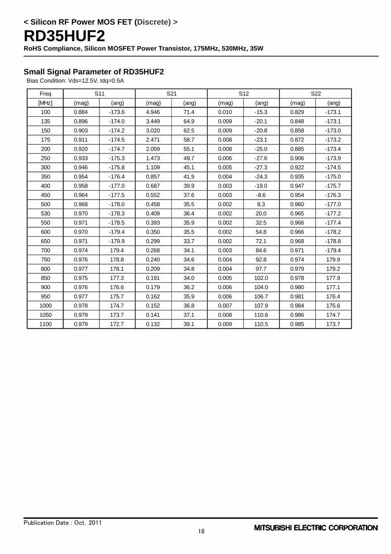
Small Signal Parameter of RD35HUF2Bias Condition: Vds=12.5V, Idq=0.5A
Freq S11 S21 S12 S22
[MHz] (mag) (ang) (mag) (ang) (mag) (ang) (mag) (ang)
100 0.884 -173.6 4.946 71.4 0.010 -15.3 0.829 -173.1
135 0.896 -174.0 3.449 64.9 0.009 -20.1 0.848 -173.1
150 0.903 -174.2 3.020 62.5 0.009 -20.8 0.858 -173.0
175 0.911 -174.5 2.471 58.7 0.008 -23.1 0.872 -173.2
200 0.920 -174.7 2.059 55.1 0.008 -25.0 0.885 -173.4
250 0.933 -175.3 1.473 49.7 0.006 -27.6 0.906 -173.9
300 0.946 -175.8 1.109 45.1 0.005 -27.3 0.922 -174.5
350 0.954 -176.4 0.857 41.9 0.004 -24.3 0.935 -175.0
400 0.958 -177.0 0.687 39.9 0.003 -19.0 0.947 -175.7
450 0.964 -177.5 0.552 37.6 0.003 -8.6 0.954 -176.3
500 0.968 -178.0 0.458 35.5 0.002 8.3 0.960 -177.0
530 0.970 -178.3 0.409 36.4 0.002 20.0 0.965 -177.2
550 0.971 -178.5 0.393 35.9 0.002 32.5 0.966 -177.4
600 0.970 -179.4 0.350 35.5 0.002 54.8 0.966 -178.2
650 0.971 -179.9 0.299 33.7 0.002 72.1 0.968 -178.8
700 0.974 179.4 0.268 34.1 0.003 84.6 0.971 -179.4
750 0.976 178.8 0.240 34.6 0.004 92.8 0.974 179.9
800 0.977 178.1 0.209 34.8 0.004 97.7 0.979 179.2
850 0.975 177.3 0.191 34.0 0.005 102.0 0.978 177.9
900 0.976 176.6 0.179 36.2 0.006 104.0 0.980 177.1
950 0.977 175.7 0.162 35.9 0.006 106.7 0.981 176.4
1000 0.978 174.7 0.152 36.8 0.007 107.9 0.984 175.6
1050 0.979 173.7 0.141 37.1 0.008 110.6 0.986 174.7
1100 0.979 172.7 0.132 39.1 0.009 110.5 0.985 173.7
< Silicon RF Power MOS FET (Discrete) >
RD35HUF2RoHS Compliance, Silicon MOSFET Power Transistor, 175MHz, 530MHz, 35W
Publication Date : Oct.2011
19
ATTENTION:1.High Temperature ; This product might have a heat generation while operation,Please take notice that have
a possibility to receive a burn to touch the operating product directly or touch the product until cold after switchoff. At the near the product,do not place the combustible material that have possibilities to arise the fire.
2.Generation of High Frequency Power ; This product generate a high frequency power. Please take noticethat do not leakage the unnecessary electric wave and use this products without cause damage for human andproperty per normal operation.
3.Before use; Before use the product,Please design the equipment in consideration of the risk for human andelectric wave obstacle for equipment.
PRECAUTIONS FOR THE USE OF MITSUBISHI SILICON RF POWER DEVICES:1. The specifications of mention are not guarantee values in this data sheet. Please confirm additional details
regarding operation of these products from the formal specification sheet. For copies of the formalspecification sheets, please contact one of our sales offices.
2.RA series products (RF power amplifier modules) and RD series products (RF power transistors) are designedfor consumer mobile communication terminals and were not specifically designed for use in other applications.In particular, while these products are highly reliable for their designed purpose, they are not manufacturedunder a quality assurance testing protocol that is sufficient to guarantee the level of reliability typically deemednecessary for critical communications elements and In the application, which is base station applications andfixed station applications that operate with long term continuous transmission and a higher on-off frequencyduring transmitting, please consider the derating, the redundancy system, appropriate setting of the maintainperiod and others as needed. For the reliability report which is described about predicted operating life time ofMitsubishi Silicon RF Products , please contact Mitsubishi Electric Corporation or an authorized MitsubishiSemiconductor product distributor.
3. RD series products use MOSFET semiconductor technology. They are sensitive to ESD voltage thereforeappropriate ESD precautions are required.
4. In the case of use in below than recommended frequency, there is possibility to occur that the device isdeteriorated or destroyed due to the RF-swing exceed the breakdown voltage.
5. In order to maximize reliability of the equipment, it is better to keep the devices temperature low. It isrecommended to utilize a sufficient sized heat-sink in conjunction with other cooling methods as needed (fan,etc.) to keep the channel temperature for RD series products lower than 120deg/C(in case ofTchmax=150deg/C) ,140deg/C(in case of Tchmax=175deg/C) under standard conditions.
6. Do not use the device at the exceeded the maximum rating condition. In case of plastic molded devices, the
exceeded maximum rating condition may cause blowout, smoldering or catch fire of the molding resin due to
extreme short current flow between the drain and the source of the device. These results causes in fire or
injury.
7. For specific precautions regarding assembly of these products into the equipment, please refer to thesupplementary items in the specification sheet.
8. Warranty for the product is void if the products protective cap (lid) is removed or if the product is modified inany way from it’s original form.
9. For additional “Safety first” in your circuit design and notes regarding the materials, please refer the last pageof this data sheet.
10. Please refer to the additional precautions in the formal specification sheet.
< Silicon RF Power MOS FET (Discrete) >
RD35HUF2RoHS Compliance, Silicon MOSFET Power Transistor, 175MHz, 530MHz, 35W
Publication Date : Oct.2011
20
© 2011 MITSUBISHI ELECTRIC CORPORATION. ALL RIGHTS RESERVED.
Keep safety first in your circuit designs!
Mitsubishi Electric Corporation puts the maximum effort into making semiconductor products better and morereliable, but there is always the possibility that trouble may occur with them. Trouble with semiconductors may leadto personal injury, fire or property damage. Remember to give due consideration to safety when making your circuitdesigns, with appropriate measures such as (i) placement of substitutive, auxiliary circuits, (ii) use ofnon-flammable material or (iii) prevention against any malfunction or mishap.
Notes regarding these materials
•These materials are intended as a reference to assist our customers in the selection of the Mitsubishisemiconductor product best suited to the customer’s application; they do not convey any license under anyintellectual property rights, or any other rights, belonging to Mitsubishi Electric Corporation or a third party.
•Mitsubishi Electric Corporation assumes no responsibility for any damage, or infringement of any third-party’srights, originating in the use of any product data, diagrams, charts, programs, algorithms, or circuit applicationexamples contained in these materials.
•All information contained in these materials, including product data, diagrams, charts, programs and algorithmsrepresents information on products at the time of publication of these materials, and are subject to change byMitsubishi Electric Corporation without notice due to product improvements or other reasons. It is thereforerecommended that customers contact Mitsubishi Electric Corporation or an authorized Mitsubishi Semiconductorproduct distributor for the latest product information before purchasing a product listed herein.The information described here may contain technical inaccuracies or typographical errors. Mitsubishi ElectricCorporation assumes no responsibility for any damage, liability, or other loss rising from these inaccuracies orerrors.Please also pay attention to information published by Mitsubishi Electric Corporation by various means, includingthe Mitsubishi Semiconductor home page (http://www.MitsubishiElectric.com/).
•When using any or all of the information contained in these materials, including product data, diagrams, charts,programs, and algorithms, please be sure to evaluate all information as a total system before making a finaldecision on the applicability of the information and products. Mitsubishi Electric Corporation assumes noresponsibility for any damage, liability or other loss resulting from the information contained herein.
•Mitsubishi Electric Corporation semiconductors are not designed or manufactured for use in a device or systemthat is used under circumstances in which human life is potentially at stake. Please contact Mitsubishi ElectricCorporation or an authorized Mitsubishi Semiconductor product distributor when considering the use of a productcontained herein for any specific purposes, such as apparatus or systems for transportation, vehicular, medical,aerospace, nuclear, or undersea repeater use.
•The prior written approval of Mitsubishi Electric Corporation is necessary to reprint or reproduce in whole or in partthese materials.
•If these products or technologies are subject to the Japanese export control restrictions, they must be exportedunder a license from the Japanese government and cannot be imported into a country other than the approveddestination.Any diversion or re-export contrary to the export control laws and regulations of Japan and/or the country ofdestination is prohibited.
•Please contact Mitsubishi Electric Corporation or an authorized Mitsubishi Semiconductor product distributor forfurther details on these materials or the products contained therein.