( Infrared Spectroscopy IR (FTIR) Leonid Murin 1,2 1 Joint Institute of Solid State and...
25
Infrared Spectroscopy IR ( (FTIR) Leonid Murin 1,2 1 Joint Institute of Solid State and Joint Institute of Solid State and Semiconductor Physics, Minsk, Belarus Semiconductor Physics, Minsk, Belarus 2 Oslo University, Centre for Materials Science Oslo University, Centre for Materials Science and Nanotechnology, Oslo, Norway and Nanotechnology, Oslo, Norway
-
date post
20-Dec-2015 -
Category
Documents
-
view
228 -
download
0
Transcript of ( Infrared Spectroscopy IR (FTIR) Leonid Murin 1,2 1 Joint Institute of Solid State and...

Infrared Spectroscopy IR ((FTIR)
Leonid Murin 1,2
11 Joint Institute of Solid State and Joint Institute of Solid State and Semiconductor Physics, Minsk, BelarusSemiconductor Physics, Minsk, Belarus
22 Oslo University, Centre for Materials Science Oslo University, Centre for Materials Science
and Nanotechnology, Oslo, Norwayand Nanotechnology, Oslo, Norway

OUTLINE
• Some general notes
• Electronic transitions
• Local Vibrational Mode spectroscopy

BACKGROUND - WHAT IS MEASURED
The light transmitted through a sample of thickness d with
polished parallel surfaces is described as
where:
I0 is the light intensity incident on the sample
α is the frequency dependent absorption coefficient
R is reflectivity (R ≈ [(n-1)/(n+1)]2 ≈ 0.3 in the mid infrared)
d
d
eR
eRII
22
2
0 1
)1(
400 600 800 1000 1200 1400 1600 1800 2000
-0.2
-0.1
0.0
0.1
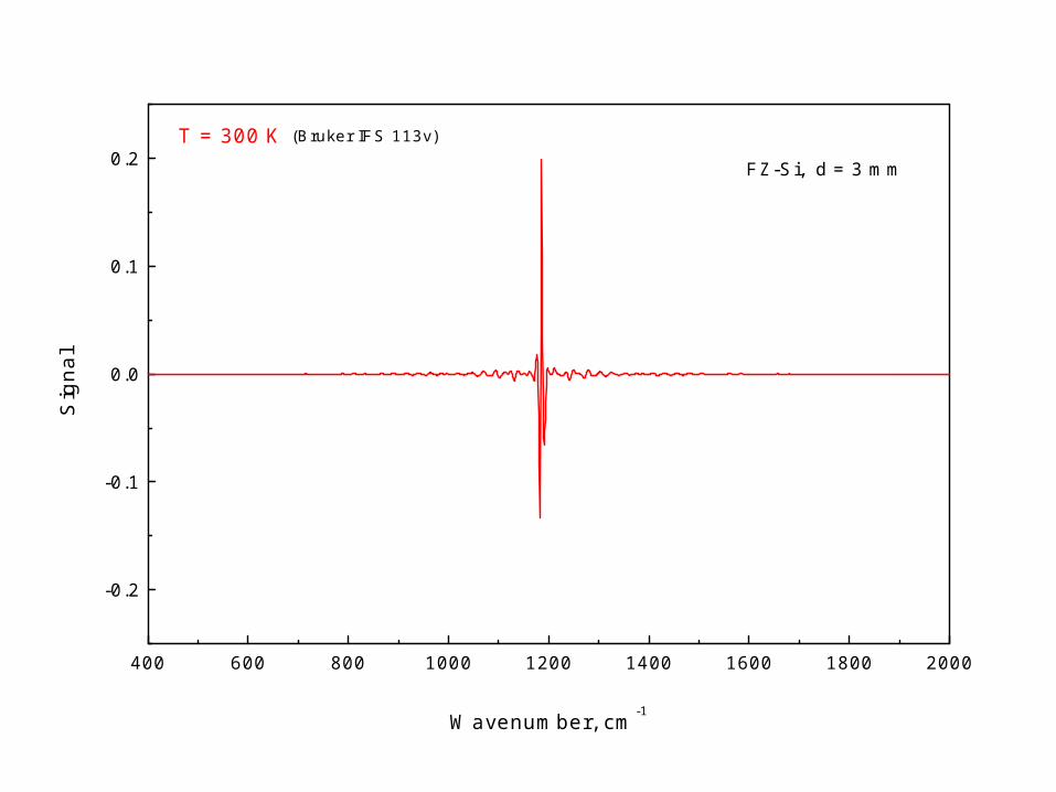
0.2(Bruker IFS 113v)T = 300 K
FZ-Si, d = 3 mm
S
igna
l
Wavenumber, cm-1

800 1000 1200 1400 1600-0.010
-0.005
0.000
0.005
0.010(Bruker IFS 113v)T = 300 K
FZ-Si, d = 3 mm
S
igna
l
Wavenumber, cm-1

400 600 800 1000 1200 1400 1600 1800 20000.0
0.1
0.2
0.3
0.4
0.5
Raw spectrumCz-3-J4, 24 GeV p-irr 1E16, d = 3 mm
Raw spectrum, FZ-Si, d = 3 mm
(Bruker IFS 113v)T = 300 KBackground (without sample)
S
igna
l
Wavenumber, cm-1

400 600 800 1000 1200 1400 1600 1800 20000.0
0.1
0.2
0.3
0.4
0.5
0.6
T = Raw spectrum of a sample / background
FZ-Si, d = 5 mm
(Bruker IFS 113v)T = 300 K
FZ-Si, d = 3 mm
T
rans
mis
sion
Wavenumber, cm-1

400 600 800 1000 1200 1400 1600 1800 20000.0
0.1
0.2
0.3
0.4
0.5
0.6
T = Raw spectrum of a sample / background
CZ-Si, 24 GeV p-irr 1x10¹⁶
cm-2, d = 3 mm
(Bruker IFS 113v)T = 300 K
FZ-Si, d = 3 mm
T
rans
mis
sion
Wavenumber, cm-1
400 600 800 1000 1200 1400 1600 1800 20000
1
2
3
4
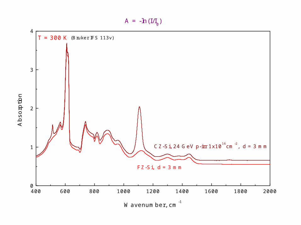
A = -ln(I/I0)
CZ-Si, 24 GeV p-irr 1x10¹⁶
cm-2, d = 3 mm
(Bruker IFS 113v)T = 300 K
FZ-Si, d = 3 mm
A
bsor
ptio
n
Wavenumber, cm-1

400 600 800 1000 1200 1400 1600 1800 20000.0
0.2
0.4
0.6
0.8
1.0
1.2
S = -ln(I/I0) - K x (-ln(I
ref/I
0))
CZ-Si, 24 GeV p-irr 1x10¹⁶
cm-2, d = 3 mm
(Bruker IFS 113v)T = 300 K
A
bsor
ptio
n
Wavenumber, cm-1

800 850 900 950 1000 10500.06
0.07
0.08
0.09
0.10
0.11
0.12
S = -ln(I/I0) - K x (-ln(I
ref/I
0))
CZ-Si, 24 GeV p-irr 1x10¹⁶
cm-2, d = 3 mm
(Bruker IFS 113v)T = 300 K
A
bsor
ptio
n
Wavenumber, cm-1

400 600 800 1000 1200 1400 1600 1800 20000.0
0.5
1.0
1.5
2.0
2.5
3.0
3.5
4.0
NO = 1.06x10¹⁸
cm-3
AC = S/d
CZ-Si, 24 GeV p-irr 1x10¹⁶
cm-2, d = 3 mm
(Bruker IFS 113v)T = 300 K
A
bsor
ptio
n co
effic
ient
, cm
-1
Wavenumber, cm-1
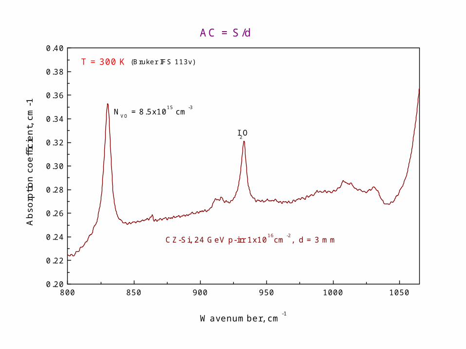
800 850 900 950 1000 10500.20
0.22
0.24
0.26
0.28
0.30
0.32
0.34
0.36
0.38
0.40
I2O
NVO = 8.5x10¹⁵
cm-3
AC = S/d
CZ-Si, 24 GeV p-irr 1x10¹⁶
cm-2, d = 3 mm
(Bruker IFS 113v)T = 300 K
A
bsor
ptio
n co
effic
ient
, cm
-1
Wavenumber, cm-1

800 850 900 950 1000 1050 1100 11500.20
0.25
0.30
0.35
0.40
0.45
Oi
O2i
O2i
IO2, I2O2
IO2, I2O2
VO
I2O
DAC = S(irrad - as-grown)/d
CZ-Si, 24 GeV p-irr 1x10¹⁶
cm-2, d = 3 mm
T = 300 K
A
bsor
ptio
n co
effic
ient
, cm
-1
Wavenumber, cm-1

800 850 900 950 1000 1050 1100
-0.2
0.0
0.2
0.4
0.6
0.8
Low temperarure measurements
3 - Cz3-J3 ([CS < 1x10¹⁵
cm-3) DAC: RT irr 1x10
16 cm
-2 p
+ 26 GeV - hot irr
2 - Cz3-J4 ([CS < 1x10¹⁵
cm-3) RT irr 1x10
16 cm
-2 p
+ 26 GeV
3
VO-
ICi
ICiOi
CiOi
IO2I2O2
I2O
I2O2
IO2
V2O2
VO
18O
i
O2i
O2i
VO2
1 - Cz1-I4 ([CS = 5x10¹⁶
cm-3) RT irr 1x10
16 cm
-2 p
+ 26 GeV
2
1
T = 20 K
A
bsor
ptio
n co
effic
ient
, cm
-1
Wavenumber, cm-1

2700 2720 2740 2760 2780 2800 2820 2840
0.0
0.2
0.4
0.6
0.8
1.0
1.5x10¹⁵
cm-3
2x10¹⁵
cm-3
3.3x10¹⁵
cm-3
4.7x10¹⁵
cm-3
4 - Cz1-I4 (C-reach, as-grown)
2 - Cz3-J4 (C-lean, as-grown)
1 - Fz1-I3 (O,C-lean, as-grown)4
3
V2 generation
RT irr 1x10¹⁶
cm-2 p
+ 24 GeV
3 - Cz3-J3 (C-lean, hot irr)
2
1
T = 20 K
A
bsor
ptio
n co
effic
ient
, cm
-1
Wavenumber, cm-1

Electronic transitions
• Shallow donors and acceptors• Group VI (S, Se, Te) etc• Thermal double donors (as an example: L.I. Murin, V.P. Markevich, J.L. Lindstrom, M. Kleverman
Spectroscopic observation of the TDD0 in silicon,
Physica B 340–342 (2003) 1046–1050).

900 1000 1100 1200 1300
0.00
0.05
0.10
0.15
3 - difference 2-12 - 300 C 2 h1 - 1250 C 40 min H2 gas
3
2
1
p-type Cz-Si ( = 80 Ohmcm)
[Oi] = 1.1x10¹⁸
cm-3
T = 15 K
TDD0 observation
TDD0O2i*O2i
O3i
OiH2
TDD1
TDD0(2p±)
TDD1(2p±)
O3i
O2i
TDD0 (2p0)TDD1 (2p0)
A
bsor
ptio
n co
effic
ient
, cm
-1
Wavenumber, cm-1
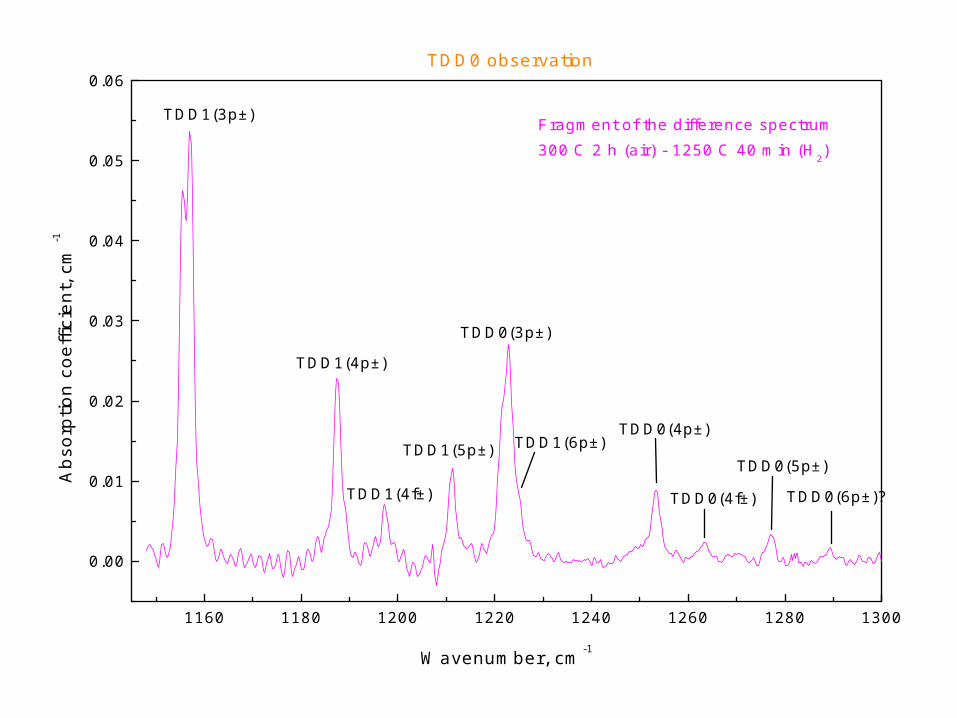
1160 1180 1200 1220 1240 1260 1280 1300
0.00
0.01
0.02
0.03
0.04
0.05
0.06TDD0 observation
TDD1(6p±)
Fragment of the difference spectrum300 C 2 h (air) - 1250 C 40 min (H2)
TDD0(6p±)?
TDD0(5p±)
TDD0(4f±)
TDD0(4p±)
TDD0(3p±)
TDD1(5p±)
TDD1(4f±)
TDD1(4p±)
TDD1(3p±)
Abs
orpt
ion
coef
ficie
nt, c
m-1
Wavenumber, cm-1

Detection limit
Calibration:
α = 1 cm-1 corresponds approximately
to NTDD = 1013 cm-3
Detection of α = 0.01 cm-1 (NTDD = 1011 cm-3) is
reliable

LVM spectroscopy
“LVM spectroscopy assumes now a very central role among the large number of semiconductor characterization techniques which have been developed over the years and which are continuously refined and improved. When applicable, this technique allows, in many cases, the precise identification of impurity species and their crystal lattice location with excellent sensitivity. Besides, LVM spectroscopy with perturbations such as polarization of the probe light, uniaxial and hydrostatic stress, and isotope substitution can be highly successful in identifying the structure and composition of various kinds of defect complexes.”
E.E Haller, Mat. Res. Soc. Symp. Proc. Vol. 378 (1995) 547-565.

Detection limits
Depend on:
Measurement temperature (LT or RT)
Sharpness of the lines
Wavenumber position
Detection limits normally are in the range
5x10¹³ – 1x1015 cm-3)
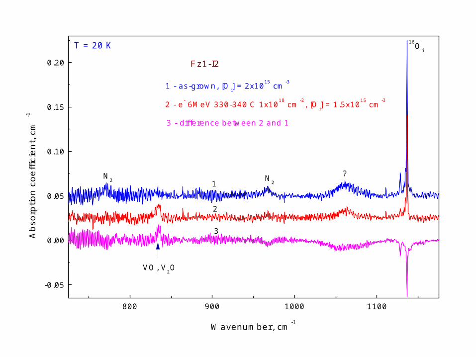
800 900 1000 1100
-0.05
0.00
0.05
0.10
0.15
0.20
?
VO, V2O
16Oi
N2N2
3
2
1
3 - difference between 2 and 1
2 - e- 6MeV 330-340 C 1x10
18 cm
-2, [Oi] = 1.5x10
15 cm
-3
1 - as-grown, [Oi] = 2x10¹⁵
cm-3
Fz1-I2
T = 20 K
A
bsor
ptio
n co
effic
ient
, cm
-1
Wavenumber, cm-1

800 850 900 950 1000 1050 1100 1150 1200-0.04
-0.02
0.00
0.02
0.04
NVO + NV2O = 5x10¹⁴
cm-3
N2
V2O
VO
Oi
Difference: RT irr 1x10¹⁶
cm-2 p
+ 24 GeV - as-grown
Fz1-I3T = 20 K
A
bsor
ptio
n co
effic
ient
, cm
-1
Wavenumber, cm-1

750 800 850 900 950 1000 1050 1100 1150 1200
0.00
0.05
0.10
0.15
0.20
N2
N2
Oi
As-grown, NO of about 2x10¹⁵
cm-3
Fz1-I3
T = 20 K
A
bsor
ptio
n co
effic
ient
, cm
-1
Wavenumber, cm-1