ELCODIS.COM - ELECTRONIC COMPONENTS...
65
1. General description NXP Semiconductors designed the LPC2458 microcontroller around a 16-bit/32-bit ARM7TDMI-S CPU core with real-time debug interfaces that include both JTAG and embedded trace. The LPC2458 has 512 kB of on-chip high-speed flash memory. This flash memory includes a special 128-bit wide memory interface and accelerator architecture that enables the CPU to execute sequential instructions from flash memory at the maximum 72 MHz system clock rate. This feature is available only on the LPC2000 ARM microcontroller family of products. The LPC2458 can execute both 32-bit ARM and 16-bit Thumb instructions. Support for the two instruction sets means engineers can choose to optimize their application for either performance or code size at the sub-routine level. When the core executes instructions in Thumb state it can reduce code size by more than 30 % with only a small loss in performance while executing instructions in ARM state maximizes core performance. The LPC2458 microcontroller is ideal for multi-purpose communication applications. It incorporates a 10/100 Ethernet Media Access Controller (MAC), a USB full-speed Device/Host/OTG Controller with 4 kB of endpoint RAM, four UARTs, two Controller Area Network (CAN) channels, an SPI interface, two Synchronous Serial Ports (SSP), three I 2 C interfaces, and an I 2 S interface. Supporting this collection of serial communications interfaces are the following feature components; an on-chip 4 MHz internal precision oscillator, 98 kB of total RAM consisting of 64 kB of local SRAM, 16 kB SRAM for Ethernet, 16 kB SRAM for general purpose DMA, 2 kB of battery powered SRAM, and an External Memory Controller (EMC). These features make this device optimally suited for communication gateways and protocol converters. Complementing the many serial communication controllers, versatile clocking capabilities, and memory features are various 32-bit timers, an improved 10-bit ADC, 10-bit DAC, two PWM units, four external interrupt pins, and up to 136 fast GPIO lines. The LPC2458 connects 64 of the GPIO pins to the hardware based Vector Interrupt Controller (VIC) that means these external inputs can generate edge-triggered interrupts. All of these features make the LPC2458 particularly suitable for industrial control and medical systems. 2. Features ARM7TDMI-S processor, running at up to 72 MHz. 512 kB on-chip flash program memory with In-System Programming (ISP) and In-Application Programming (IAP) capabilities. Flash program memory is on the ARM local bus for high performance CPU access. 98 kB on-chip SRAM includes: 64 kB of SRAM on the ARM local bus for high performance CPU access. 16 kB SRAM for Ethernet interface. Can also be used as general purpose SRAM. LPC2458 Single-chip 16-bit/32-bit micro; 512 kB flash, ethernet, CAN, ISP/IAP, USB 2.0 device/host/OTG, external memory interface Rev. 01 — 6 July 2007 Preliminary data sheet Downloaded from Elcodis.com electronic components distributor
Transcript of ELCODIS.COM - ELECTRONIC COMPONENTS...

1. General description
NXP Semiconductors designed the LPC2458 microcontroller around a 16-bit/32-bit ARM7TDMI-S CPU core with real-time debug interfaces that include both JTAG and embedded trace. The LPC2458 has 512 kB of on-chip high-speed flash memory. This flash memory includes a special 128-bit wide memory interface and accelerator architecture that enables the CPU to execute sequential instructions from flash memory at the maximum 72 MHz system clock rate. This feature is available only on the LPC2000 ARM microcontroller family of products. The LPC2458 can execute both 32-bit ARM and 16-bit Thumb instructions. Support for the two instruction sets means engineers can choose to optimize their application for either performance or code size at the sub-routine level. When the core executes instructions in Thumb state it can reduce code size by more than 30 % with only a small loss in performance while executing instructions in ARM state maximizes core performance.
The LPC2458 microcontroller is ideal for multi-purpose communication applications. It incorporates a 10/100 Ethernet Media Access Controller (MAC), a USB full-speed Device/Host/OTG Controller with 4 kB of endpoint RAM, four UARTs, two Controller Area Network (CAN) channels, an SPI interface, two Synchronous Serial Ports (SSP), three I2C interfaces, and an I2S interface. Supporting this collection of serial communications interfaces are the following feature components; an on-chip 4 MHz internal precision oscillator, 98 kB of total RAM consisting of 64 kB of local SRAM, 16 kB SRAM for Ethernet, 16 kB SRAM for general purpose DMA, 2 kB of battery powered SRAM, and an External Memory Controller (EMC). These features make this device optimally suited for communication gateways and protocol converters. Complementing the many serial communication controllers, versatile clocking capabilities, and memory features are various 32-bit timers, an improved 10-bit ADC, 10-bit DAC, two PWM units, four external interrupt pins, and up to 136 fast GPIO lines. The LPC2458 connects 64 of the GPIO pins to the hardware based Vector Interrupt Controller (VIC) that means these external inputs can generate edge-triggered interrupts. All of these features make the LPC2458 particularly suitable for industrial control and medical systems.
2. Features
� ARM7TDMI-S processor, running at up to 72 MHz.
� 512 kB on-chip flash program memory with In-System Programming (ISP) and In-Application Programming (IAP) capabilities. Flash program memory is on the ARM local bus for high performance CPU access.
� 98 kB on-chip SRAM includes:
� 64 kB of SRAM on the ARM local bus for high performance CPU access.
� 16 kB SRAM for Ethernet interface. Can also be used as general purpose SRAM.
LPC2458Single-chip 16-bit/32-bit micro; 512 kB flash, ethernet, CAN, ISP/IAP, USB 2.0 devi ce/host/OTG, external memo ry in terfaceRev. 01 — 6 July 2007 Prelim inary dat a sheet
Downloaded from Elcodis.com electronic components distributor
LPC2468_1 © NXP B.V. 2007. All rights reserved.
Prelim inary da ta sheet Rev. 01 — 6 July 2007 2 of 65
NXP Semiconductors LPC2458Fast communica tion ch ip
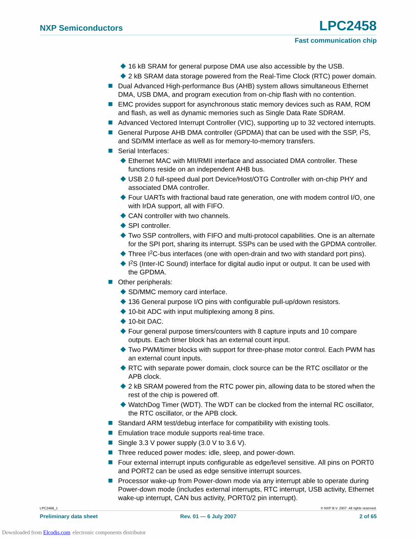
� 16 kB SRAM for general purpose DMA use also accessible by the USB.
� 2 kB SRAM data storage powered from the Real-Time Clock (RTC) power domain.
� Dual Advanced High-performance Bus (AHB) system allows simultaneous Ethernet DMA, USB DMA, and program execution from on-chip flash with no contention.
� EMC provides support for asynchronous static memory devices such as RAM, ROM and flash, as well as dynamic memories such as Single Data Rate SDRAM.
� Advanced Vectored Interrupt Controller (VIC), supporting up to 32 vectored interrupts.
� General Purpose AHB DMA controller (GPDMA) that can be used with the SSP, I2S, and SD/MM interface as well as for memory-to-memory transfers.
� Serial Interfaces:
� Ethernet MAC with MII/RMII interface and associated DMA controller. These functions reside on an independent AHB bus.
� USB 2.0 full-speed dual port Device/Host/OTG Controller with on-chip PHY and associated DMA controller.
� Four UARTs with fractional baud rate generation, one with modem control I/O, one with IrDA support, all with FIFO.
� CAN controller with two channels.
� SPI controller.
� Two SSP controllers, with FIFO and multi-protocol capabilities. One is an alternate for the SPI port, sharing its interrupt. SSPs can be used with the GPDMA controller.
� Three I2C-bus interfaces (one with open-drain and two with standard port pins).
� I2S (Inter-IC Sound) interface for digital audio input or output. It can be used with the GPDMA.
� Other peripherals:
� SD/MMC memory card interface.
� 136 General purpose I/O pins with configurable pull-up/down resistors.
� 10-bit ADC with input multiplexing among 8 pins.
� 10-bit DAC.
� Four general purpose timers/counters with 8 capture inputs and 10 compare outputs. Each timer block has an external count input.
� Two PWM/timer blocks with support for three-phase motor control. Each PWM has an external count inputs.
� RTC with separate power domain, clock source can be the RTC oscillator or the APB clock.
� 2 kB SRAM powered from the RTC power pin, allowing data to be stored when the rest of the chip is powered off.
� WatchDog Timer (WDT). The WDT can be clocked from the internal RC oscillator, the RTC oscillator, or the APB clock.
� Standard ARM test/debug interface for compatibility with existing tools.
� Emulation trace module supports real-time trace.
� Single 3.3 V power supply (3.0 V to 3.6 V).
� Three reduced power modes: idle, sleep, and power-down.
� Four external interrupt inputs configurable as edge/level sensitive. All pins on PORT0 and PORT2 can be used as edge sensitive interrupt sources.
� Processor wake-up from Power-down mode via any interrupt able to operate during Power-down mode (includes external interrupts, RTC interrupt, USB activity, Ethernet wake-up interrupt, CAN bus activity, PORT0/2 pin interrupt).
Downloaded from Elcodis.com electronic components distributor

LPC2468_1 © NXP B.V. 2007. All rights reserved.
Prelim inary da ta sheet Rev. 01 — 6 July 2007 3 of 65
NXP Semiconductors LPC2458Fast communica tion ch ip
� Two independent power domains allow fine tuning of power consumption based on needed features.
� Each peripheral has its own clock divider for further power saving. These dividers help reducing active power by 20 - 30 %.
� Brownout detect with separate thresholds for interrupt and forced reset.
� On-chip power-on reset.
� On-chip crystal oscillator with an operating range of 1 MHz to 24 MHz.
� 4 MHz internal RC oscillator trimmed to 1 % accuracy that can optionally be used as the system clock. When used as the CPU clock, does not allow CAN and USB to run.
� On-chip PLL allows CPU operation up to the maximum CPU rate without the need for a high frequency crystal. May be run from the main oscillator, the internal RC oscillator, or the RTC oscillator.
� Boundary scan for simplified board testing.
� Versatile pin function selections allow more possibilities for using on-chip peripheral functions.
3. Applications
� Industrial control
� Medical systems
� Protocol converter
� Communications
4. Ordering information
4.1 Ordering options
Table 1. Ordering informatio n
Type number Package
Name Descr ip tio n Version
LPC2458FET180 TFBGA180 plastic thin fine-pitch ball grid array package; 180 balls; body 12 x 12 x 0.8 mm SOT570-2
Table 2. Ordering options
Type number Flash (kB)
SRAM (kB) External bus
Ethernet USB OTG/ OHC/ DEV + 4 kB FIFO
CA
N c
hann
els
SD/MMC
GP DMA
AD
C c
hann
els
DA
C c
hann
els
Temp range
Loca
l bu
s
Eth
erne
t bu
ffer
GP
/US
B
RT
C
Tota
l
LPC2458FET180 512 64 16 16 2 98 Full 32-bit MII/RMII
yes 2 yes yes 8 1 �40 qC to +85 qC
Downloaded from Elcodis.com electronic components distributor

LPC2468_1 © NXP B.V. 2007. All rights reserved.
Prelim inary da ta sheet Rev. 01 — 6 July 2007 4 of 65
NXP Semiconductors LPC2458Fast communica tion ch ip
5. Block diagram
Fig 1. LPC2458 blo ck diag ram
power domain 2
LPC2458
A[19:0]
D[15:0]EXTERNAL
MEMORY
CONTROLLER
ALARM
002aad093
PWM0, PWM1
ARM7TDMI-S
PLL
EINT3 to EINT0
FLASH
P3, P4
P0, P1, P2,
LEGACY GPI/O
64 PINS TOTALP0, P1
SCK, SCK0MOSI, MOSI0
SSEL, SSEL1
SCK1MOSI1
MIS01SSEL1
SCL0, SCL1, SCL2
I2SRX_CLKI2STX_CLK
I2SRX_WSI2STX_WS
8 u�AD0
RTCX1
RTCX2
MCICLK, MCIPWR
RXD0, RXD2, RXD3
TXD1RXD1
RD1, RD2TD1, TD2
CAN1, CAN2
port1
XTAL1
TCK TDOEXTIN0
XTAL2
RESETTRST
TDITMS
HIGH-SPEED
GPI/O
136 PINS
TOTAL
port2
64 kB
SRAM
512 kB
FLASH
INTERNAL
CONTROLLERS
TEST/DEBUG
INTERFACE
EM
UL
AT
ION
TR
AC
E M
OD
UL
E
trace signals
AHB
BRIDGE
AHB
BRIDGE
ETHERNET
MAC WITH
DMA
16 kB
SRAMMASTER
PORT
AHB TO
APB BRIDGE
SLAVE
PORT
system
clock
SYSTEM
FUNCTIONS
INTERNAL RC
OSCILLATOR
VDDA
VDD(3V3)
VDD(DCDC)(3V3)
VDD(1V8)
VREF
VSSA, VSS
VIC16 kB
SRAM
USB DEVICE/
HOST/OTG WITH
4 kB RAM AND DMA
GP DMA
CONTROLLER
I2S INTERFACE
SPI, SSP0 INTERFACE
I2SRX_SDA
I2STX_SDA
MISO, MISO0
SSP1 INTERFACE
SD/MMC CARD
INTERFACE MCICMD,
MCIDAT[3:0]
TXD0, TXD2, TXD3UART0, UART2, UART3
UART1 DTR1, RTS1
DSR1, CTS1, DCD1,
RI1
I2C0, I2C1, I2C2 SDA0, SDA1, SDA2
EXTERNAL INTERRUPTS
CAPTURE/COMPARE
TIMER0/TIMER1/
TIMER2/TIMER3
A/D CONVERTER
D/A CONVERTER
2 kB BATTERY RAM
RTC
OSCILLATOR
REAL-
TIME
CLOCK
WATCHDOG TIMER
SYSTEM CONTROL
2 u CAP0/CAP1/
CAP2/CAP3
4 u MAT2,
2 u MAT3,
2 u�MAT1/MAT0
6 u PWM0, PWM1
1 u�PCAP0,
2 u�PCAP1
AOUT
VBAT
AHB TO
APB BRIDGE
SRAM
MII/RMII
VBUS
DBGEN
P0, P2
AHB2 AHB1
control lines
Downloaded from Elcodis.com electronic components distributor

LPC2468_1 © NXP B.V. 2007. All rights reserved.
Prelim inary da ta sheet Rev. 01 — 6 July 2007 5 of 65
NXP Semiconductors LPC2458Fast communica tion ch ip
6. Pinning information
6.1 Pinning
Fig 2. LPC2458 pin ning TFBGA180 package
002aad094
LPC2458
2 4 6 8 10 12 13 141 3 5 7 9 11
ball A1
index area
P
N
M
L
K
J
G
E
H
F
D
C
B
A
Transparent top view
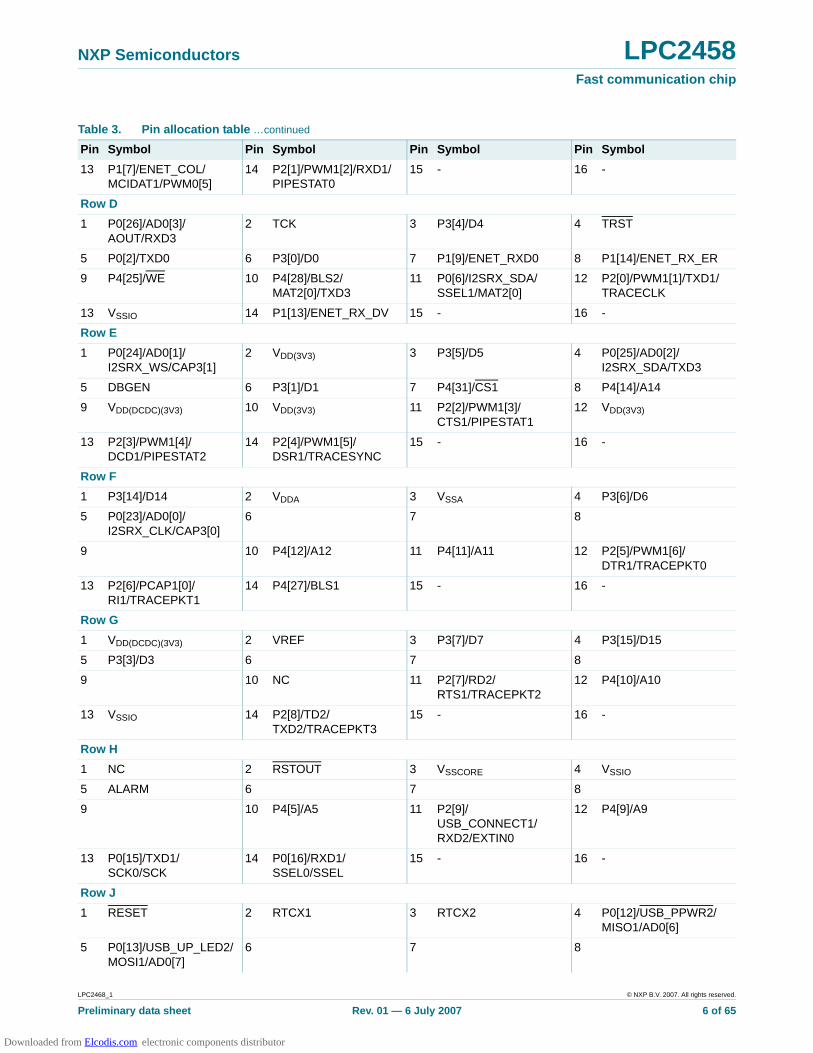
Table 3. Pin allo catio n table
Pin Symbol Pin Symbol Pin Symbol Pin Symbol
Row A
1 P3[12]/D12 2 P3[2]/D2 3 P0[3]/RXD0 4 P3[9]/D9
5 P1[1]/ENET_TXD1 6 P3[8]/D8 7 P1[10]/ENET_RXD1 8 P1[15]/ENET_REF_CLK/ENET_RX_CLK
9 P1[3]/ENET_TXD3/MCICMD/PWM0[2]
10 VSSCORE 11 P0[4]/I2SRX_CLK/RD2/CAP2[0]
12 P1[11]/ENET_RXD2/MCIDAT2/PWM0[6]
13 P0[9]/I2STX_SDA/MOSI1/MAT2[3]
14 P1[12]/ENET_RXD3/MCIDAT3/PCAP0[0]
15 - 16 -
Row B
1 TDO 2 P3[11]/D11 3 P3[10]/D10 4 VSSIO
5 P1[0]/ENET_TXD0 6 P1[8]/ENET_CRS_DV/ENET_CRS
7 P1[2]/ENET_TXD2/MCICLK/PWM0[1]
8 P1[16]/ENET_MDC
9 P4[29]/BLS3/MAT2[1]/RXD3
10 P1[6]/ENET_TX_CLK/MCIDAT0/PWM0[4]
11 P0[5]/I2SRX_WS/TD2/CAP2[1]
12 P0[7]/I2STX_CLK/SCK1/MAT2[1]
13 P1[5]/ENET_TX_ER/MCIPWR/PWM0[3]
14 P4[13]/A13 15 - 16 -
Row C
1 P3[13]/D13 2 TMS 3 TDI 4 RTCK
5 VDD(3V3) 6 P1[4]/ENET_TX_EN 7 P4[30]/CS0 8 P4[24]/OE
9 P1[17]/ENET_MDIO 10 P4[15]/A15 11 VSSIO 12 P0[8]/I2STX_WS/MISO1/MAT2[2]
Downloaded from Elcodis.com electronic components distributor
LPC2468_1 © NXP B.V. 2007. All rights reserved.
Prelim inary da ta sheet Rev. 01 — 6 July 2007 6 of 65
NXP Semiconductors LPC2458Fast communica tion ch ip
13 P1[7]/ENET_COL/MCIDAT1/PWM0[5]
14 P2[1]/PWM1[2]/RXD1/PIPESTAT0
15 - 16 -
Row D
1 P0[26]/AD0[3]/AOUT/RXD3
2 TCK 3 P3[4]/D4 4 TRST
5 P0[2]/TXD0 6 P3[0]/D0 7 P1[9]/ENET_RXD0 8 P1[14]/ENET_RX_ER
9 P4[25]/WE 10 P4[28]/BLS2/MAT2[0]/TXD3
11 P0[6]/I2SRX_SDA/SSEL1/MAT2[0]
12 P2[0]/PWM1[1]/TXD1/TRACECLK
13 VSSIO 14 P1[13]/ENET_RX_DV 15 - 16 -
Row E
1 P0[24]/AD0[1]/I2SRX_WS/CAP3[1]
2 VDD(3V3) 3 P3[5]/D5 4 P0[25]/AD0[2]/I2SRX_SDA/TXD3
5 DBGEN 6 P3[1]/D1 7 P4[31]/CS1 8 P4[14]/A14
9 VDD(DCDC)(3V3) 10 VDD(3V3) 11 P2[2]/PWM1[3]/CTS1/PIPESTAT1
12 VDD(3V3)
13 P2[3]/PWM1[4]/DCD1/PIPESTAT2
14 P2[4]/PWM1[5]/DSR1/TRACESYNC
15 - 16 -
Row F
1 P3[14]/D14 2 VDDA 3 VSSA 4 P3[6]/D6
5 P0[23]/AD0[0]/I2SRX_CLK/CAP3[0]
6 7 8
9 10 P4[12]/A12 11 P4[11]/A11 12 P2[5]/PWM1[6]/DTR1/TRACEPKT0
13 P2[6]/PCAP1[0]/RI1/TRACEPKT1
14 P4[27]/BLS1 15 - 16 -
Row G
1 VDD(DCDC)(3V3) 2 VREF 3 P3[7]/D7 4 P3[15]/D15
5 P3[3]/D3 6 7 8
9 10 NC 11 P2[7]/RD2/RTS1/TRACEPKT2
12 P4[10]/A10
13 VSSIO 14 P2[8]/TD2/TXD2/TRACEPKT3
15 - 16 -
Row H
1 NC 2 RSTOUT 3 VSSCORE 4 VSSIO
5 ALARM 6 7 8
9 10 P4[5]/A5 11 P2[9]/USB_CONNECT1/RXD2/EXTIN0
12 P4[9]/A9
13 P0[15]/TXD1/SCK0/SCK
14 P0[16]/RXD1/SSEL0/SSEL
15 - 16 -
Row J
1 RESET 2 RTCX1 3 RTCX2 4 P0[12]/USB_PPWR2/MISO1/AD0[6]
5 P0[13]/USB_UP_LED2/MOSI1/AD0[7]
6 7 8
Table 3. Pin allo catio n table …continued
Pin Symbol Pin Symbol Pin Symbol Pin Symbol
Downloaded from Elcodis.com electronic components distributor

LPC2468_1 © NXP B.V. 2007. All rights reserved.
Prelim inary da ta sheet Rev. 01 — 6 July 2007 7 of 65
NXP Semiconductors LPC2458Fast communica tion ch ip
9 10 P0[19]/DSR1/MCICLK/SDA1
11 P4[8]/A8 12 P0[17]/CTS1/MISO0/MISO
13 P0[18]/DCD1/MOSI0/MOSI
14 VDD(3V3) 15 - 16 -
Row K
1 VBAT 2 P1[31]/USB_OVRCR2/SCK1/AD0[5]
3 P1[30]/USB_PWRD2/VBUS/AD0[4]
4 XTAL2
5 P0[29]/USB_D+1 6 P1[20]/USB_TX_DP1/PWM1[2]/SCK0
7 P3[26]/D26/MAT0[1]/PWM1[3]
8 VDD(3V3)
9 P4[3]/A3 10 P4[6]/A6 11 P0[21]/RI1/MCIPWR/RD1
12 P4[7]/A7
13 P4[26]/BLS0 14 P0[20]/DTR1/MCICMD/SCL1
15 - 16 -
Row L
1 P2[29]/DQMOUT1 2 XTAL1 3 P0[27]/SDA0 4 VDD(3V3)
5 P1[18]/USB_UP_LED1/PWM1[1]/CAP1[0]
6 P4[0]/A0 7 P1[25]/USB_LS1/USB_HSTEN1/MAT1[1]
8 VSSCORE
9 VSSIO 10 P0[10]/TXD2/SDA2/MAT3[0]
11 VDD(3V3) 12 NC
13 VSSIO 14 P0[22]/RTS1/MCIDAT0/TD1
15 - 16 -
Row M
1 P0[28]/SCL0 2 P2[28]/DQMOUT0 3 P3[25]/D25/MAT0[0]/PWM1[2]
4 P3[23]/D23/CAP0[0]/PCAP1[0]
5 P0[14]/USB_HSTEN2/USB_CONNECT2/SSEL1
6 P1[22]/USB_RCV1/USB_PWRD1/MAT1[0]
7 P4[1]/A1 8 P4[2]/A2
9 P1[27]/USB_INT1/USB_OVRCR1/CAP0[1]
10 P0[0]/RD1/TXD3/SDA1 11 P2[13]/EINT3/MCIDAT3/I2STX_SDA
12 P2[11]/EINT1/MCIDAT1/I2STX_CLK
13 P2[10]/EINT0 14 P4[19]/A19 15 - 16 -
Row N
1 P0[31]/USB_D+2 2 USB_D�2 3 P3[24]/D24/CAP0[1]/PWM1[1]
4 P0[30]/USB_D�1
5 P2[19]/CLKOUT1 6 P1[21]/USB_TX_DM1/PWM1[3]/SSEL0
7 P1[23]/USB_RX_DP1/PWM1[4]/MISO0
8 P2[21]/DYCS1
9 VDD(DCDC)(3V3) 10 P1[29]/USB_SDA1/PCAP1[1]/MAT0[1]
11 P0[1]/TD1/RXD3/SCL1 12 P4[16]/A16
13 P4[17]/A17 14 P2[12]/EINT2/MCIDAT2/I2STX_WS
15 - 16 -
Row P
1 P2[24]/CKEOUT0 2 P2[25]/CKEOUT1 3 P2[18]/CLKOUT0 4 VSSIO
5 P1[19]/USB_TX_E1/USB_PPWR1/CAP1[1]
6 P2[20]/DYCS0 7 P1[24]/USB_RX_DM1/PWM1[5]/MOSI0
8 P1[26]/USB_SSPND1/PWM1[6]/CAP0[0]
9 P2[16]/CAS 10 P1[28]/USB_SCL1/PCAP1[0]/MAT0[0]
11 P2[17]/RAS 12 P0[11]/RXD2/SCL2/MAT3[1]
13 P4[4]/A4 14 P4[18]/A18 15 - 16 -
Table 3. Pin allo catio n table …continued
Pin Symbol Pin Symbol Pin Symbol Pin Symbol
Downloaded from Elcodis.com electronic components distributor

LPC2468_1 © NXP B.V. 2007. All rights reserved.
Prelim inary da ta sheet Rev. 01 — 6 July 2007 8 of 65
NXP Semiconductors LPC2458Fast communica tion ch ip
6.2 Pin d escrip tion
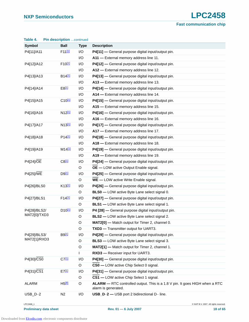
Table 4. Pin de scr ip tio n
Symbol Ball Type Description
P0[0] to P0[31] I/O Port 0: Port 0 is a 32-bit I/O port with individual direction controls for each bit. The operation of port 0 pins depends upon the pin function selected via the Pin Connect block.
P0[0]/RD1/TXD3/SDA1
M10[1] I/O P0[0] — General purpose digital input/output pin.
I RD1 — CAN1 receiver input.
O TXD3 — Transmitter output for UART3.
I/O SDA1 — I2C1 data input/output (this is not an open-drain pin).
P0[1]/TD1/RXD3/SCL1
N11[1] I/O P0[1] — General purpose digital input/output pin.
O TD1 — CAN1 transmitter output.
I RXD3 — Receiver input for UART3.
I/O SCL1 — I2C1 clock input/output (this is not an open-drain pin).
P0[2]/TXD0 D5[1] I/O P0[2] — General purpose digital input/output pin.
O TXD0 — Transmitter output for UART0.
P0[3]/RXD0 A3[1] I/O P0[3] — General purpose digital input/output pin.
I RXD0 — Receiver input for UART0.
P0[4]/I2SRX_CLK/RD2/CAP2[0]
A11[1] I/O P0[4] — General purpose digital input/output pin.
I/O I2SRX_CLK — Receive Clock. It is driven by the master and received by the slave. Corresponds to the signal SCK in the I2S-bus specification.
I RD2 — CAN2 receiver input.
I CAP2[0] — Capture input for Timer 2, channel 0.
P0[5]/I2SRX_WS/TD2/CAP2[1]
B11[1] I/O P0[5] — General purpose digital input/output pin.
I/O I2SRX_WS — Receive Word Select. It is driven by the master and received by the slave. Corresponds to the signal WS in the I2S-bus specification.
O TD2 — CAN2 transmitter output.
I CAP2[1] — Capture input for Timer 2, channel 1.
P0[6]/I2SRX_SDA/SSEL1/MAT2[0]
D11[1] I/O P0[6] — General purpose digital input/output pin.
I/O I2SRX_SDA — Receive data. It is driven by the transmitter and read by the receiver. Corresponds to the signal SD in the I2S-bus specification.
I/O SSEL1 — Slave Select for SSP1.
O MAT2[0] — Match output for Timer 2, channel 0.
P0[7]/I2STX_CLK/SCK1/MAT2[1]
B12[1] I/O P0[7] — General purpose digital input/output pin.
I/O I2STX_CLK — Transmit Clock. It is driven by the master and received by the slave. Corresponds to the signal SCK in the I2S-bus specification.
I/O SCK1 — Serial Clock for SSP1.
O MAT2[1] — Match output for Timer 2, channel 1.
P0[8]/I2STX_WS/MISO1/MAT2[2]
C12[1] I/O P0[8] — General purpose digital input/output pin.
I/O I2STX_WS — Transmit Word Select. It is driven by the master and received by the slave. Corresponds to the signal WS in the I2S-bus specification.
I/O MISO1 — Master In Slave Out for SSP1.
O MAT2[2] — Match output for Timer 2, channel 2.
Downloaded from Elcodis.com electronic components distributor
LPC2468_1 © NXP B.V. 2007. All rights reserved.
Prelim inary da ta sheet Rev. 01 — 6 July 2007 9 of 65
NXP Semiconductors LPC2458Fast communica tion ch ip
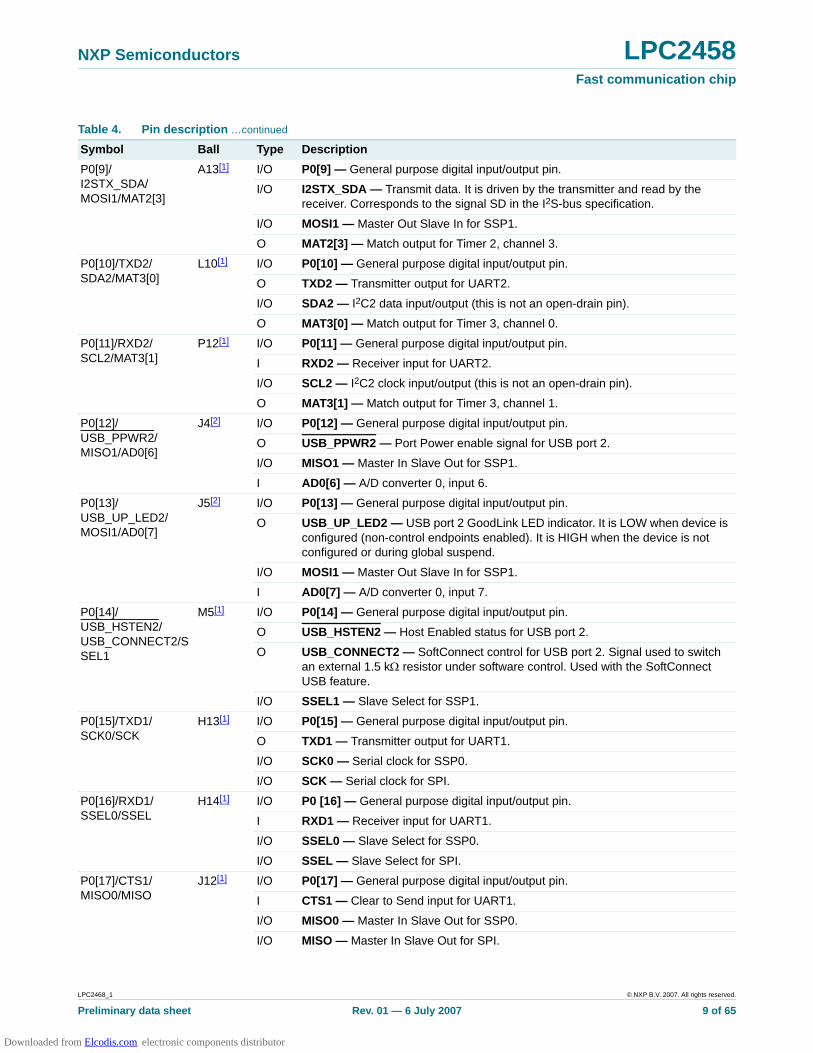
P0[9]/I2STX_SDA/MOSI1/MAT2[3]
A13[1] I/O P0[9] — General purpose digital input/output pin.
I/O I2STX_SDA — Transmit data. It is driven by the transmitter and read by the receiver. Corresponds to the signal SD in the I2S-bus specification.
I/O MOSI1 — Master Out Slave In for SSP1.
O MAT2[3] — Match output for Timer 2, channel 3.
P0[10]/TXD2/SDA2/MAT3[0]
L10[1] I/O P0[10] — General purpose digital input/output pin.
O TXD2 — Transmitter output for UART2.
I/O SDA2 — I2C2 data input/output (this is not an open-drain pin).
O MAT3[0] — Match output for Timer 3, channel 0.
P0[11]/RXD2/SCL2/MAT3[1]
P12[1] I/O P0[11] — General purpose digital input/output pin.
I RXD2 — Receiver input for UART2.
I/O SCL2 — I2C2 clock input/output (this is not an open-drain pin).
O MAT3[1] — Match output for Timer 3, channel 1.
P0[12]/USB_PPWR2/MISO1/AD0[6]
J4[2] I/O P0[12] — General purpose digital input/output pin.
O USB_PPWR2 — Port Power enable signal for USB port 2.
I/O MISO1 — Master In Slave Out for SSP1.
I AD0[6] — A/D converter 0, input 6.
P0[13]/USB_UP_LED2/MOSI1/AD0[7]
J5[2] I/O P0[13] — General purpose digital input/output pin.
O USB_UP_LED2 — USB port 2 GoodLink LED indicator. It is LOW when device is configured (non-control endpoints enabled). It is HIGH when the device is not configured or during global suspend.
I/O MOSI1 — Master Out Slave In for SSP1.
I AD0[7] — A/D converter 0, input 7.
P0[14]/USB_HSTEN2/USB_CONNECT2/SSEL1
M5[1] I/O P0[14] — General purpose digital input/output pin.
O USB_HSTEN2 — Host Enabled status for USB port 2.
O USB_CONNECT2 — SoftConnect control for USB port 2. Signal used to switch an external 1.5 k: resistor under software control. Used with the SoftConnect USB feature.
I/O SSEL1 — Slave Select for SSP1.
P0[15]/TXD1/SCK0/SCK
H13[1] I/O P0[15] — General purpose digital input/output pin.
O TXD1 — Transmitter output for UART1.
I/O SCK0 — Serial clock for SSP0.
I/O SCK — Serial clock for SPI.
P0[16]/RXD1/SSEL0/SSEL
H14[1] I/O P0 [16] — General purpose digital input/output pin.
I RXD1 — Receiver input for UART1.
I/O SSEL0 — Slave Select for SSP0.
I/O SSEL — Slave Select for SPI.
P0[17]/CTS1/MISO0/MISO
J12[1] I/O P0[17] — General purpose digital input/output pin.
I CTS1 — Clear to Send input for UART1.
I/O MISO0 — Master In Slave Out for SSP0.
I/O MISO — Master In Slave Out for SPI.
Table 4. Pin de scr ip tio n …continued
Symbol Ball Type Description
Downloaded from Elcodis.com electronic components distributor

LPC2468_1 © NXP B.V. 2007. All rights reserved.
Prelim inary da ta sheet Rev. 01 — 6 July 2007 10 of 65
NXP Semiconductors LPC2458Fast communica tion ch ip
P0[18]/DCD1/MOSI0/MOSI
J13[1] I/O P0[18] — General purpose digital input/output pin.
I DCD1 — Data Carrier Detect input for UART1.
I/O MOSI0 — Master Out Slave In for SSP0.
I/O MOSI — Master Out Slave In for SPI.
P0[19]/DSR1/MCICLK/SDA1
J10[1] I/O P0[19] — General purpose digital input/output pin.
I DSR1 — Data Set Ready input for UART1.
O MCICLK — Clock output line for SD/MMC interface.
I/O SDA1 — I2C1 data input/output (this is not an open-drain pin).
P0[20]/DTR1/MCICMD/SCL1
K14[1] I/O P0[20] — General purpose digital input/output pin.
O DTR1 — Data Terminal Ready output for UART1.
I/O MCICMD — Command line for SD/MMC interface.
I/O SCL1 — I2C1 clock input/output (this is not an open-drain pin).
P0[21]/RI1/MCIPWR/RD1
K11[1] I/O P0[21] — General purpose digital input/output pin.
I RI1 — Ring Indicator input for UART1.
O MCIPWR — Power Supply Enable for external SD/MMC power supply.
I RD1 — CAN1 receiver input.
P0[22]/RTS1/MCIDAT0/TD1
L14[1] I/O P0[22] — General purpose digital input/output pin.
O RTS1 — Request to Send output for UART1.
I/O MCIDAT0 — Data line 0 for SD/MMC interface.
O TD1 — CAN1 transmitter output.
P0[23]/AD0[0]/I2SRX_CLK/CAP3[0]
F5[2] I/O P0[23] — General purpose digital input/output pin.
I AD0[0] — A/D converter 0, input 0.
I/O I2SRX_CLK — Receive Clock. It is driven by the master and received by the slave. Corresponds to the signal SCK in the I2S-bus specification.
I CAP3[0] — Capture input for Timer 3, channel 0.
P0[24]/AD0[1]/I2SRX_WS/CAP3[1]
E1[2] I/O P0[24] — General purpose digital input/output pin.
I AD0[1] — A/D converter 0, input 1.
I/O I2SRX_WS — Receive Word Select. It is driven by the master and received by the slave. Corresponds to the signal WS in the I2S-bus specification.
I CAP3[1] — Capture input for Timer 3, channel 1.
P0[25]/AD0[2]/I2SRX_SDA/TXD3
E4[2] I/O P0[25] — General purpose digital input/output pin.
I AD0[2] — A/D converter 0, input 2.
I/O I2SRX_SDA — Receive data. It is driven by the transmitter and read by the receiver. Corresponds to the signal SD in the I2S-bus specification.
O TXD3 — Transmitter output for UART3.
P0[26]/AD0[3]/AOUT/RXD3
D1[2][3] I/O P0[26] — General purpose digital input/output pin.
I AD0[3] — A/D converter 0, input 3.
O AOUT — D/A converter output.
I RXD3 — Receiver input for UART3.
P0[27]/SDA0 L3[4] I/O P0[27] — General purpose digital input/output pin.
I/O SDA0 — I2C0 data input/output. Open-drain output (for I2C-bus compliance).
Table 4. Pin de scr ip tio n …continued
Symbol Ball Type Description
Downloaded from Elcodis.com electronic components distributor

LPC2468_1 © NXP B.V. 2007. All rights reserved.
Prelim inary da ta sheet Rev. 01 — 6 July 2007 11 of 65
NXP Semiconductors LPC2458Fast communica tion ch ip
P0[28]/SCL0 M1[4] I/O P0[28] — General purpose digital input/output pin.
I/O SCL0 — I2C0 clock input/output. Open-drain output (for I2C-bus compliance).
P0[29]/USB_D+1 K5[5] I/O P0[29] — General purpose digital input/output pin.
I/O USB_D+1 — USB port 1 bidirectional D+ line.
P0[30]/USB_D�1 N4[5] I/O P0[30] — General purpose digital input/output pin.
I/O USB_D�1 — USB port 1bidirectional D� line.
P0[31]/USB_D+2 N1[5] I/O P0[31] — General purpose digital input/output pin.
I/O USB_D+2 — USB port 2 bidirectional D+ line.
P1[0] to P1[31] I/O Port 1: Port 1 is a 32 bit I/O port with individual direction controls for each bit. The operation of port 1 pins depends upon the pin function selected via the Pin Connect block.
P1[0]/ENET_TXD0
B5[1] I/O P1[0] — General purpose digital input/output pin.
O ENET_TXD0 — Ethernet transmit data 0 (RMII/MII interface).
P1[1]/ENET_TXD1
A5[1] I/O P1[1] — General purpose digital input/output pin.
O ENET_TXD1 — Ethernet transmit data 1 (RMII/MII interface).
P1[2]/ENET_TXD2/MCICLK/PWM0[1]
B7[1] I/O P1[2] — General purpose digital input/output pin.
O ENET_TXD2 — Ethernet transmit data 2 (MII interface).
O MCICLK — Clock output line for SD/MMC interface.
O PWM0[1] — Pulse Width Modulator 0, output 1.
P1[3]/ENET_TXD3/MCICMD/PWM0[2]
A9[1] I/O P1[3] — General purpose digital input/output pin.
O ENET_TXD3 — Ethernet transmit data 3 (MII interface).
I/O MCICMD — Command line for SD/MMC interface.
O PWM0[2] — Pulse Width Modulator 0, output 2.
P1[4]/ENET_TX_EN
C6[1] I/O P1[4] — General purpose digital input/output pin.
O ENET_TX_EN — Ethernet transmit data enable (RMII/MII interface).
P1[5]/ENET_TX_ER/MCIPWR/PWM0[3]
B13[1] I/O P1[5] — General purpose digital input/output pin.
O ENET_TX_ER — Ethernet Trensmit Error (MII interface).
O MCIPWR — Power Supply Enable for external SD/MMC power supply.
O PWM0[3] — Pulse Width Modulator 0, output 3.
P1[6]/ENET_TX_CLK/MCIDAT0/PWM0[4]
B10[1] I/O P1[6] — General purpose digital input/output pin.
I ENET_TX_CLK — Ethernet Transmit Clock (MII interface).
I/O MCIDAT0 — Data line 0 for SD/MMC interface.
O PWM0[4] — Pulse Width Modulator 0, output 4.
P1[7]/ENET_COL/MCIDAT1/PWM0[5]
C13[1] I/O P1[7] — General purpose digital input/output pin.
I ENET_COL — Ethernet Collision detect (MII interface).
I/O MCIDAT1 — Data line 1 for SD/MMC interface.
O PWM0[5] — Pulse Width Modulator 0, output 5.
P1[8]/ENET_CRS_DV/ENET_CRS
B6[1] I/O P1[8] — General purpose digital input/output pin.
I ENET_CRS_DV/ENET_CRS — Ethernet Carrier Sense/Data Valid (RMII interface)/ Ethernet Carrier Sense (MII interface).
P1[9]/ENET_RXD0
D7[1] I/O P1[9] — General purpose digital input/output pin.
I ENET_RXD0 — Ethernet receive data 0 (RMII/MII interface).
Table 4. Pin de scr ip tio n …continued
Symbol Ball Type Description
Downloaded from Elcodis.com electronic components distributor

LPC2468_1 © NXP B.V. 2007. All rights reserved.
Prelim inary da ta sheet Rev. 01 — 6 July 2007 12 of 65
NXP Semiconductors LPC2458Fast communica tion ch ip
P1[10]/ENET_RXD1
A7[1] I/O P1[10] — General purpose digital input/output pin.
I ENET_RXD1 — Ethernet receive data 1 (RMII/MII interface).
P1[11]/ENET_RXD2/MCIDAT2/PWM0[6]
A12[1] I/O P1[11] — General purpose digital input/output pin.
I ENET_RXD2 — Ethernet Receive Data 2 (MII interface).
I/O MCIDAT2 — Data line 2 for SD/MMC interface.
O PWM0[6] — Pulse Width Modulator 0, output 6.
P1[12]/ENET_RXD3/MCIDAT3/PCAP0[0]
A14[1] I/O P1[12] — General purpose digital input/output pin.
I ENET_RXD3 — Ethernet Receive Data (MII interface).
I/O MCIDAT3 — Data line 3 for SD/MMC interface.
I PCAP0[0] — Capture input for PWM0, channel 0.
P1[13]/ENET_RX_DV
D14[1] I/O P1[13] — General purpose digital input/output pin.
I ENET_RX_DV — Ethernet Receive Data Valid (MII interface).
P1[14]/ENET_RX_ER
D8[1] I/O P1[14] — General purpose digital input/output pin.
I ENET_RX_ER — Ethernet receive error (RMII/MII interface).
P1[15]/ENET_REF_CLK/ENET_RX_CLK
A8[1] I/O P1[15] — General purpose digital input/output pin.
I ENET_REF_CLK/ENET_RX_CLK — Ethernet Reference Clock (RMII interface)/ Ethernet Receive Clock (MII interface).
P1[16]/ENET_MDC
B8[1] I/O P1[16] — General purpose digital input/output pin.
I ENET_MDC — Ethernet MIIM clock.
P1[17]/ENET_MDIO
C9[1] I/O P1[17] — General purpose digital input/output pin.
I/O ENET_MDIO — Ethernet MI data input and output.
P1[18]/USB_UP_LED1/PWM1[1]/CAP1[0]
L5[1] I/O P1[18] — General purpose digital input/output pin.
O USB_UP_LED1 — USB port 1 GoodLink LED indicator. It is LOW when device is configured (non-control endpoints enabled). It is HIGH when the device is not configured or during global suspend.
O PWM1[1] — Pulse Width Modulator 1, channel 1 output.
I CAP1[0] — Capture input for Timer 1, channel 0.
P1[19]/USB_TX_E1/USB_PPWR1/CAP1[1]
P5[1] I/O P1[19] — General purpose digital input/output pin.
O USB_TX_E1 — Transmit Enable signal for USB port 1 (OTG transceiver).
O USB_PPWR1 — Port Power enable signal for USB port 1.
I CAP1[1] — Capture input for Timer 1, channel 1.
P1[20]/USB_TX_DP1/PWM1[2]/SCK0
K6[1] I/O P1[20] — General purpose digital input/output pin.
O USB_TX_DP1 — D+ transmit data for USB port 1 (OTG transceiver).
O PWM1[2] — Pulse Width Modulator 1, channel 2 output.
I/O SCK0 — Serial clock for SSP0.
P1[21]/USB_TX_DM1/PWM1[3]/SSEL0
N6[1] I/O P1[21] — General purpose digital input/output pin.
O USB_TX_DM1 — D� transmit data for USB port 1 (OTG transceiver).
O PWM1[3] — Pulse Width Modulator 1, channel 3 output.
I/O SSEL0 — Slave Select for SSP0.
Table 4. Pin de scr ip tio n …continued
Symbol Ball Type Description
Downloaded from Elcodis.com electronic components distributor

LPC2468_1 © NXP B.V. 2007. All rights reserved.
Prelim inary da ta sheet Rev. 01 — 6 July 2007 13 of 65
NXP Semiconductors LPC2458Fast communica tion ch ip
P1[22]/USB_RCV1/USB_PWRD1/MAT1[0]
M6[1] I/O P1[22] — General purpose digital input/output pin.
I USB_RCV1 — Differential receive data for USB port 1 (OTG transceiver).
I USB_PWRD1 — Power Status for USB port 1 (host power switch).
O MAT1[0] — Match output for Timer 1, channel 0.
P1[23]/USB_RX_DP1/PWM1[4]/MISO0
N7[1] I/O P1[23] — General purpose digital input/output pin.
I USB_RX_DP1 — D+ receive data for USB port 1 (OTG transceiver).
O PWM1[4] — Pulse Width Modulator 1, channel 4 output.
I/O MISO0 — Master In Slave Out for SSP0.
P1[24]/USB_RX_DM1/PWM1[5]/MOSI0
P7[1] I/O P1[24] — General purpose digital input/output pin.
I USB_RX_DM1 — D� receive data for USB port 1 (OTG transceiver).
O PWM1[5] — Pulse Width Modulator 1, channel 5 output.
I/O MOSI0 — Master Out Slave in for SSP0.
P1[25]/USB_LS1/USB_HSTEN1/MAT1[1]
L7[1] I/O P1[25] — General purpose digital input/output pin.
O USB_LS1 — Low-speed status for USB port 1 (OTG transceiver).
O USB_HSTEN1 — Host Enabled status for USB port 1.
O MAT1[1] — Match output for Timer 1, channel 1.
P1[26]/USB_SSPND1/PWM1[6]/CAP0[0]
P8[1] I/O P1[26] — General purpose digital input/output pin.
O USB_SSPND1 — USB port 1 Bus Suspend status (OTG transciever).
O PWM1[6] — Pulse Width Modulator 1, channel 6 output.
I CAP0[0] — Capture input for Timer 0, channel 0.
P1[27]/USB_INT1/USB_OVRCR1/CAP0[1]
M9[1] I/O P1[27] — General purpose digital input/output pin.
I USB_INT1 — USB port 1 OTG ATX interrupt (OTG transceiver).
I USB_OVRCR1 — USB port 1 Over-Current status.
I CAP0[1] — Capture input for Timer 0, channel 1.
P1[28]/USB_SCL1/PCAP1[0]/MAT0[0]
P10[1] I/O P1[28] — General purpose digital input/output pin.
I/O USB_SCL1 — USB port 1 I2C serial clock (OTG transciever).
I PCAP1[0] — Capture input for PWM1, channel 0.
O MAT0[0] — Match output for Timer 0, channel 0.
P1[29]/USB_SDA1/PCAP1[1]/MAT0[1]
N10[1] I/O P1[29] — General purpose digital input/output pin.
I/O USB_SDA1 — USB port 1 I2C serial data (OTG transciever).
I PCAP1[1] — Capture input for PWM1, channel 1.
O MAT0[1] — Match output for Timer 0, channel 0.
P1[30]/USB_PWRD2/VBUS/AD0[4]
K3[2] I/O P1[30] — General purpose digital input/output pin.
I USB_PWRD2 — Power Status for USB port 2.
I VBUS — Indicates the presence of USB bus power.
Note: This signal must be HIGH for USB reset to occur.
I AD0[4] — A/D converter 0, input 4.
P1[31]/USB_OVRCR2/SCK1/AD0[5]
K2[2] I/O P1[31] — General purpose digital input/output pin.
I USB_OVRCR2 — Over-Current status for USB port 2.
I/O SCK1 — Serial Clock for SSP1.
I AD0[5] — A/D converter 0, input 5.
Table 4. Pin de scr ip tio n …continued
Symbol Ball Type Description
Downloaded from Elcodis.com electronic components distributor

LPC2468_1 © NXP B.V. 2007. All rights reserved.
Prelim inary da ta sheet Rev. 01 — 6 July 2007 14 of 65
NXP Semiconductors LPC2458Fast communica tion ch ip
P2[0] to P2[31] I/O Port 2: Port 2 is a 32-bit I/O port with individual direction controls for each bit. The operation of port 2 pins depends upon the pin function selected via the Pin Connect block.
P2[0]/PWM1[1]/TXD1/TRACECLK
D12[1] I/O P2[0] — General purpose digital input/output pin.
O PWM1[1] — Pulse Width Modulator 1, channel 1 output.
O TXD1 — Transmitter output for UART1.
O TRACECLK — Trace Clock.
P2[1]/PWM1[2]/RXD1/PIPESTAT0
C14[1] I/O P2[1] — General purpose digital input/output pin.
O PWM1[2] — Pulse Width Modulator 1, channel 2 output.
I RXD1 — Receiver input for UART1.
O PIPESTAT0 — Pipeline Status, bit 0.
P2[2]/PWM1[3]/CTS1/PIPESTAT1
E11[1] I/O P2[2] — General purpose digital input/output pin.
O PWM1[3] — Pulse Width Modulator 1, channel 3 output.
I CTS1 — Clear to Send input for UART1.
O PIPESTAT1 — Pipeline Status, bit 1.
P2[3]/PWM1[4]/DCD1/PIPESTAT2
E13[1] I/O P2[3] — General purpose digital input/output pin.
O PWM1[4] — Pulse Width Modulator 1, channel 4 output.
I DCD1 — Data Carrier Detect input for UART1.
O PIPESTAT2 — Pipeline Status, bit 2.
P2[4]/PWM1[5]/DSR1/TRACESYNC
E14[1] I/O P2[4] — General purpose digital input/output pin.
O PWM1[5] — Pulse Width Modulator 1, channel 5 output.
I DSR1 — Data Set Ready input for UART1.
O TRACESYNC — Trace Synchronization.
P2[5]/PWM1[6]/DTR1/TRACEPKT0
F12[1] I/O P2[5] — General purpose digital input/output pin.
O PWM1[6] — Pulse Width Modulator 1, channel 6 output.
O DTR1 — Data Terminal Ready output for UART1.
O TRACEPKT0 — Trace Packet, bit 0.
P2[6]/PCAP1[0]/RI1/TRACEPKT1
F13[1] I/O P2[6] — General purpose digital input/output pin.
I PCAP1[0] — Capture input for PWM1, channel 0.
I RI1 — Ring Indicator input for UART1.
O TRACEPKT1 — Trace Packet, bit 1.
P2[7]/RD2/RTS1/TRACEPKT2
G11[1] I/O P2[7] — General purpose digital input/output pin.
I RD2 — CAN2 receiver input.
O RTS1 — Request to Send output for UART1.
O TRACEPKT2 — Trace Packet, bit 2.
P2[8]/TD2/TXD2/TRACEPKT3
G14[1] I/O P2[8] — General purpose digital input/output pin.
O TD2 — CAN2 transmitter output.
O TXD2 — Transmitter output for UART2.
O TRACEPKT3 — Trace Packet, bit 3.
Table 4. Pin de scr ip tio n …continued
Symbol Ball Type Description
Downloaded from Elcodis.com electronic components distributor

LPC2468_1 © NXP B.V. 2007. All rights reserved.
Prelim inary da ta sheet Rev. 01 — 6 July 2007 15 of 65
NXP Semiconductors LPC2458Fast communica tion ch ip
P2[9]/USB_CONNECT1/RXD2/EXTIN0
H11[1] I/O P2[9] — General purpose digital input/output pin.
O USB_CONNECT1 — USB1 SoftConnect control. Signal used to switch an external 1.5 k: resistor under the software control. Used with the SoftConnect USB feature.
I RXD2 — Receiver input for UART2.
I EXTIN0 — External Trigger Input.
P2[10]/EINT0 M13[6] I/O P2[10] — General purpose digital input/output pin.
Note: LOW on this pin while RESET is LOW forces on-chip bootloader to take over control of the part after a reset.
I EINT0 — External interrupt 0 input.
P2[11]/EINT1/MCIDAT1/I2STX_CLK
M12[6] I/O P2[11] — General purpose digital input/output pin.
I EINT1 — External interrupt 1 input.
I/O MCIDAT1 — Data line 1 for SD/MMC interface.
I/O I2STX_CLK — Transmit Clock. It is driven by the master and received by the slave. Corresponds to the signal SCK in the I2S-bus specification.
P2[12]/EINT2/MCIDAT2/I2STX_WS
N14[6] I/O P2[12] — General purpose digital input/output pin.
I EINT2 — External interrupt 2 input.
I/O MCIDAT2 — Data line 2 for SD/MMC interface.
I/O I2STX_WS — Transmit Word Select. It is driven by the master and received by the slave. Corresponds to the signal WS in the I2S-bus specification.
P2[13]/EINT3/MCIDAT3/I2STX_SDA
M11[6] I/O P2[13] — General purpose digital input/output pin.
I EINT3 — External interrupt 3 input.
I/O MCIDAT3 — Data line 3 for SD/MMC interface.
I/O I2STX_SDA — Transmit data. It is driven by the transmitter and read by the receiver. Corresponds to the signal SD in the I2S-bus specification.
P2[16]/CAS P9[1] I/O P2[16] — General purpose digital input/output pin.
O CAS — LOW active SDRAM Column Address Strobe.
P2[17]/RAS P11[1] I/O P2[17] — General purpose digital input/output pin.
O RAS — LOW active SDRAM Row Address Strobe.
P2[18]/CLKOUT0
P3[1] I/O P2[18] — General purpose digital input/output pin.
O CLKOUT0 — SDRAM clock 0.
P2[19]/CLKOUT1
N5[1] I/O P2[19] — General purpose digital input/output pin.
O CLKOUT1 — SDRAM clock 1.
P2[20]/DYCS0 P6[1] I/O P2[20] — General purpose digital input/output pin.
O DYCS0 — SDRAM chip select 0.
P2[21]/DYCS1 N8[1] I/O P2[21] — General purpose digital input/output pin.
O DYCS1 — SDRAM chip select 1.
P2[24]/CKEOUT0
P1[1] I/O P2[24] — General purpose digital input/output pin.
O CKEOUT0 — SDRAM clock enable 0.
P2[25]/CKEOUT1
P2[1] I/O P2[25] — General purpose digital input/output pin.
O CKEOUT1 — SDRAM clock enable 1.
Table 4. Pin de scr ip tio n …continued
Symbol Ball Type Description
Downloaded from Elcodis.com electronic components distributor
LPC2468_1 © NXP B.V. 2007. All rights reserved.
Prelim inary da ta sheet Rev. 01 — 6 July 2007 16 of 65
NXP Semiconductors LPC2458Fast communica tion ch ip
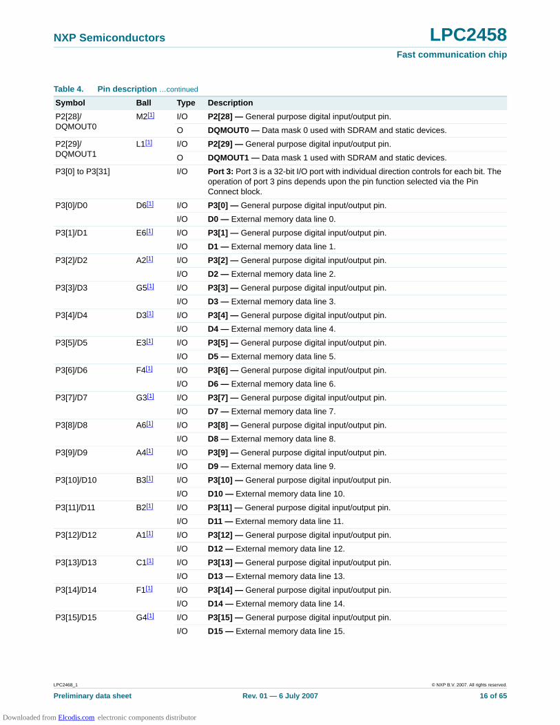
P2[28]/DQMOUT0
M2[1] I/O P2[28] — General purpose digital input/output pin.
O DQMOUT0 — Data mask 0 used with SDRAM and static devices.
P2[29]/DQMOUT1
L1[1] I/O P2[29] — General purpose digital input/output pin.
O DQMOUT1 — Data mask 1 used with SDRAM and static devices.
P3[0] to P3[31] I/O Port 3: Port 3 is a 32-bit I/O port with individual direction controls for each bit. The operation of port 3 pins depends upon the pin function selected via the Pin Connect block.
P3[0]/D0 D6[1] I/O P3[0] — General purpose digital input/output pin.
I/O D0 — External memory data line 0.
P3[1]/D1 E6[1] I/O P3[1] — General purpose digital input/output pin.
I/O D1 — External memory data line 1.
P3[2]/D2 A2[1] I/O P3[2] — General purpose digital input/output pin.
I/O D2 — External memory data line 2.
P3[3]/D3 G5[1] I/O P3[3] — General purpose digital input/output pin.
I/O D3 — External memory data line 3.
P3[4]/D4 D3[1] I/O P3[4] — General purpose digital input/output pin.
I/O D4 — External memory data line 4.
P3[5]/D5 E3[1] I/O P3[5] — General purpose digital input/output pin.
I/O D5 — External memory data line 5.
P3[6]/D6 F4[1] I/O P3[6] — General purpose digital input/output pin.
I/O D6 — External memory data line 6.
P3[7]/D7 G3[1] I/O P3[7] — General purpose digital input/output pin.
I/O D7 — External memory data line 7.
P3[8]/D8 A6[1] I/O P3[8] — General purpose digital input/output pin.
I/O D8 — External memory data line 8.
P3[9]/D9 A4[1] I/O P3[9] — General purpose digital input/output pin.
I/O D9 — External memory data line 9.
P3[10]/D10 B3[1] I/O P3[10] — General purpose digital input/output pin.
I/O D10 — External memory data line 10.
P3[11]/D11 B2[1] I/O P3[11] — General purpose digital input/output pin.
I/O D11 — External memory data line 11.
P3[12]/D12 A1[1] I/O P3[12] — General purpose digital input/output pin.
I/O D12 — External memory data line 12.
P3[13]/D13 C1[1] I/O P3[13] — General purpose digital input/output pin.
I/O D13 — External memory data line 13.
P3[14]/D14 F1[1] I/O P3[14] — General purpose digital input/output pin.
I/O D14 — External memory data line 14.
P3[15]/D15 G4[1] I/O P3[15] — General purpose digital input/output pin.
I/O D15 — External memory data line 15.
Table 4. Pin de scr ip tio n …continued
Symbol Ball Type Description
Downloaded from Elcodis.com electronic components distributor

LPC2468_1 © NXP B.V. 2007. All rights reserved.
Prelim inary da ta sheet Rev. 01 — 6 July 2007 17 of 65
NXP Semiconductors LPC2458Fast communica tion ch ip
P3[23]/D23/CAP0[0]/PCAP1[0]
M4[1] I/O P3[23] — General purpose digital input/output pin.
I/O D23 — External memory data line 23.
I CAP0[0] — Capture input for Timer 0, channel 0.
I PCAP1[0] — Capture input for PWM1, channel 0.
P3[24]/D24/CAP0[1]/PWM1[1]
N3[1] I/O P3[24] — General purpose digital input/output pin.
I/O D24 — External memory data line 24.
I CAP0[1] — Capture input for Timer 0, channel 1.
O PWM1[1] — Pulse Width Modulator 1, output 1.
P3[25]/D25/MAT0[0]/PWM1[2]
M3[1] I/O P3[25] — General purpose digital input/output pin.
I/O D25 — External memory data line 25.
O MAT0[0] — Match output for Timer 0, channel 0.
O PWM1[2] — Pulse Width Modulator 1, output 2.
P3[26]/D26/MAT0[1]/PWM1[3]
K7[1] I/O P3[26] — General purpose digital input/output pin.
I/O D26 — External memory data line 26.
O MAT0[1] — Match output for Timer 0, channel 1.
O PWM1[3] — Pulse Width Modulator 1, output 3.
P4[0] to P4[31] I/O Port 4: Port 4 is a 32-bit I/O port with individual direction controls for each bit. The operation of port 4 pins depends upon the pin function selected via the Pin Connect block.
P4[0]/A0 L6[1] I/O P4[0] — ]General purpose digital input/output pin.
I/O A0 — External memory address line 0.
P4[1]/A1 M7[1] I/O P4[1] — General purpose digital input/output pin.
I/O A1 — External memory address line 1.
P4[2]/A2 M8[1] I/O P4[2] — General purpose digital input/output pin.
I/O A2 — External memory address line 2.
P4[3]/A3 K9[1] I/O P4[3] — General purpose digital input/output pin.
I/O A3 — External memory address line 3.
P4[4]/A4 P13[1] I/O P4[4] — General purpose digital input/output pin.
I/O A4 — External memory address line 4.
P4[5]/A5 H10[1] I/O P4[5] — General purpose digital input/output pin.
I/O A5 — External memory address line 5.
P4[6]/A6 K10[1] I/O P4[6] — General purpose digital input/output pin.
I/O A6 — External memory address line 6.
P4[7]/A7 K12[1] I/O P4[7] — General purpose digital input/output pin.
I/O A7 — External memory address line 7.
P4[8]/A8 J11[1] I/O P4[8] — General purpose digital input/output pin.
I/O A8 — External memory address line 8.
P4[9]/A9 H12[1] I/O P4[9] — General purpose digital input/output pin.
I/O A9 — External memory address line 9.
P4[10]/A10 G12[1] I/O P4[10] — General purpose digital input/output pin.
I/O A10 — External memory address line 10.
Table 4. Pin de scr ip tio n …continued
Symbol Ball Type Description
Downloaded from Elcodis.com electronic components distributor
LPC2468_1 © NXP B.V. 2007. All rights reserved.
Prelim inary da ta sheet Rev. 01 — 6 July 2007 18 of 65
NXP Semiconductors LPC2458Fast communica tion ch ip
P4[11]/A11 F11[1] I/O P4[11] — General purpose digital input/output pin.
I/O A11 — External memory address line 11.
P4[12]/A12 F10[1] I/O P4[12] — General purpose digital input/output pin.
I/O A12 — External memory address line 12.
P4[13]/A13 B14[1] I/O P4[13] — General purpose digital input/output pin.
I/O A13 — External memory address line 13.
P4[14]/A14 E8[1] I/O P4[14] — General purpose digital input/output pin.
I/O A14 — External memory address line 14.
P4[15]/A15 C10[1] I/O P4[15] — General purpose digital input/output pin.
I/O A15 — External memory address line 15.
P4[16]/A16 N12[1] I/O P4[16] — General purpose digital input/output pin.
I/O A16 — External memory address line 16.
P4[17]/A17 N13[1] I/O P4[17] — General purpose digital input/output pin.
I/O A17 — External memory address line 17.
P4[18]/A18 P14[1] I/O P4[18] — General purpose digital input/output pin.
I/O A18 — External memory address line 18.
P4[19]/A19 M14[1] I/O P4[19] — General purpose digital input/output pin.
I/O A19 — External memory address line 19.
P4[24]/OE C8[1] I/O P4[24] — General purpose digital input/output pin.
O OE — LOW active Output Enable signal.
P4[25]/WE D9[1] I/O P4[25] — General purpose digital input/output pin.
O WE — LOW active Write Enable signal.
P4[26]/BLS0 K13[1] I/O P4[26] — General purpose digital input/output pin.
O BLS0 — LOW active Byte Lane select signal 0.
P4[27]/BLS1 F14[1] I/O P4[27] — General purpose digital input/output pin.
O BLS1 — LOW active Byte Lane select signal 1.
P4[28]/BLS2/MAT2[0]/TXD3
D10[1] I/O P4 [28] — General purpose digital input/output pin.
O BLS2 — LOW active Byte Lane select signal 2.
O MAT2[0] — Match output for Timer 2, channel 0.
O TXD3 — Transmitter output for UART3.
P4[29]/BLS3/MAT2[1]/RXD3
B9[1] I/O P4[29] — General purpose digital input/output pin.
O BLS3 — LOW active Byte Lane select signal 3.
O MAT2[1] — Match output for Timer 2, channel 1.
I RXD3 — Receiver input for UART3.
P4[30]/CS0 C7[1] I/O P4[30] — General purpose digital input/output pin.
O CS0 — LOW active Chip Select 0 signal.
P4[31]/CS1 E7[1] I/O P4[31] — General purpose digital input/output pin.
O CS1 — LOW active Chip Select 1 signal.
ALARM H5[8] O ALA RM — RTC controlled output. This is a 1.8 V pin. It goes HIGH when a RTC alarm is generated.
USB_D�2 N2 I/O USB_D�2 — USB port 2 bidirectional D� line.
Table 4. Pin de scr ip tio n …continued
Symbol Ball Type Description
Downloaded from Elcodis.com electronic components distributor

LPC2468_1 © NXP B.V. 2007. All rights reserved.
Prelim inary da ta sheet Rev. 01 — 6 July 2007 19 of 65
NXP Semiconductors LPC2458Fast communica tion ch ip
[1] 5 V tolerant pad providing digital I/O functions with TTL levels and hysteresis.
DBGEN E5[1] I DBGEN — JTAG interface control signal. Also used for boundary scanning.
TDO B1[1] O TDO — Test Data out for JTAG interface.
TDI C3[1] I TDI — Test Data in for JTAG interface.
TMS C2[1] I TMS — Test Mode Select for JTAG interface.
TRST D4[1] I TRST — Test Reset for JTAG interface.
TCK D2[1] I TCK — Test Clock for JTAG interface.
RTCK C4[1] I/O RTCK — JTAG interface control signal.
Note: LOW on this pin while RESET is LOW enables ETM pins (P2[9:0]) to operate as Trace port after reset.
RSTOUT H2[1] O RSTOUT — LOW on this pin indicates LPC2458 being in Reset state.
RESET J1[7] I exter nal reset input: A LOW on this pin resets the device, causing I/O ports and peripherals to take on their default states, and processor execution to begin at address 0. TTL with hysteresis, 5 V tolerant.
The VBAT pin must be powered with 3.3 V for the RESET pin to detect external signal existence and/or activity.
XTAL1 L2[8] I Input to the oscillator circuit and internal clock generator circuits.
XTAL2 K4[8] O Output from the oscillator amplifier.
RTCX1 J2[8] I Input to the RTC oscillator circuit.
RTCX2 J3[8] O Output from the RTC oscillator circuit.
VSSIO H4, P4,L9, L13, G13,D13, C11, B4[9]
I groun d: 0 V reference for the digital IO pins.
VSSCORE H3, L8, A10[9]
I groun d: 0 V reference for the core.
VSSA F3[10] I analog gro und : 0 V reference. This should nominally be the same voltage as VSS, but should be isolated to minimize noise and error.
VDD(3V3) E2,L4,K8,L11,J14, E12, E10,C5[1
1]
I 3.3 V supply volt age: This is the power supply voltage for the I/O ports.
NC H1, L12, G10[12]
I Not Co nnected pins : These pins must be left unconnected (floating).
VDD(DCDC)(3V3) G1, N9, E9[13]
I 3.3 V DC-to-DC con ver ter su pply voltage: This is the power supply for the on-chip DC-to-DC converter.
VDDA F2[14] I analog 3.3 V pad su pply vo ltage: This should be nominally the same voltage as VDD(3V3) but should be isolated to minimize noise and error. This voltage is used to power the ADC and DAC.
VREF G2[14] I ADC refe rence: This should be nominally the same voltage as VDD(3V3) but should be isolated to minimize noise and error. The level on this pin is used as a reference for ADC and DAC.
VBAT K1[14] I RTC and RESET pin power su pply : 3.3 V on this pin supplies the power to the RTC peripheral and the RESET pin logic.
Table 4. Pin de scr ip tio n …continued
Symbol Ball Type Description
Downloaded from Elcodis.com electronic components distributor

LPC2468_1 © NXP B.V. 2007. All rights reserved.
Prelim inary da ta sheet Rev. 01 — 6 July 2007 20 of 65
NXP Semiconductors LPC2458Fast communica tion ch ip
[2] 5 V tolerant pad providing digital I/O functions (with TTL levels and hysteresis) and analog input. When configured as a ADC input, digital section of the pad is disabled.
[3] 5 V tolerant pad providing digital I/O with TTL levels and hysteresis and analog output function. When configured as the DAC output, digital section of the pad is disabled.
[4] Open-drain 5 V tolerant digital I/O I2C-bus 400 kHz specification compatible pad. It requires an external pull-up to provide output functionality. When power is switched off, this pin connected to the I2C-bus is floating and does not disturb the I2C lines.
[5] Pad provides digital I/O and USB functions. It is designed in accordance with the USB specification, revision 2.0 (Full-speed and Low-speed mode only).
[6] 5 V tolerant pad with 5 ns glitch filter providing digital I/O functions with TTL levels and hysteresis.
[7] 5 V tolerant pad with 20 ns glitch filter providing digital I/O function with TTL levels and hysteresis.
[8] Pad provides special analog functionality.
[9] Pad provides special analog functionality.
[10] Pad provides special analog functionality.
[11] Pad provides special analog functionality.
[12] Pad provides special analog functionality.
[13] Pad provides special analog functionality.
[14] Pad provides special analog functionality.
7. Functional description
7.1 Architectural o verviewThe LPC2458 microcontroller consists of an ARM7TDMI-S CPU with emulation support, the ARM7 local bus for closely coupled, high-speed access to the majority of on-chip memory, the AMBA AHB interfacing to high-speed on-chip peripherals and external memory, and the AMBA APB for connection to other on-chip peripheral functions. The microcontroller permanently configures the ARM7TDMI-S processor for little-endian byte order.
The LPC2458 implements two AHB buses in order to allow the Ethernet block to operate without interference caused by other system activity. The primary AHB, referred to as AHB1, includes the VIC, GPDMA controller, and EMC.
The second AHB, referred to as AHB2, includes only the Ethernet block and an associated 16 kB SRAM. In addition, a bus bridge is provided that allows the secondary AHB to be a bus master on AHB1, allowing expansion of Ethernet buffer space into off-chip memory or unused space in memory residing on AHB1.
In summary, bus masters with access to AHB1 are the ARM7 itself, the GPDMA function, and the Ethernet block (via the bus bridge from AHB2). Bus masters with access to AHB2 are the ARM7 and the Ethernet block.
AHB peripherals are allocated a 2 MB range of addresses at the very top of the 4 GB ARM memory space. Each AHB peripheral is allocated a 16 kB address space within the AHB address space. Lower speed peripheral functions are connected to the APB bus. The AHB to APB bridge interfaces the APB bus to the AHB bus. APB peripherals are also allocated a 2 MB range of addresses, beginning at the 3.5 GB address point. Each APB peripheral is allocated a 16 kB address space within the APB address space.
The ARM7TDMI-S processor is a general purpose 32-bit microprocessor, which offers high performance and very low power consumption. The ARM architecture is based on Reduced Instruction Set Computer (RISC) principles, and the instruction set and related
Downloaded from Elcodis.com electronic components distributor

LPC2468_1 © NXP B.V. 2007. All rights reserved.
Prelim inary da ta sheet Rev. 01 — 6 July 2007 21 of 65
NXP Semiconductors LPC2458Fast communica tion ch ip
decode mechanism are much simpler than those of microprogrammed complex instruction set computers. This simplicity results in a high instruction throughput and impressive real-time interrupt response from a small and cost-effective processor core.
Pipeline techniques are employed so that all parts of the processing and memory systems can operate continuously. Typically, while one instruction is being executed, its successor is being decoded, and a third instruction is being fetched from memory.
The ARM7TDMI-S processor also employs a unique architectural strategy known as Thumb, which makes it ideally suited to high-volume applications with memory restrictions, or applications where code density is an issue.
The key idea behind Thumb is that of a super-reduced instruction set. Essentially, the ARM7TDMI-S processor has two instruction sets:
• the standard 32-bit ARM set
• a 16-bit Thumb set
The Thumb set’s 16-bit instruction length allows it to approach higher density compared to standard ARM code while retaining most of the ARM’s performance.
7.2 On-chip flash p rogramming memoryThe LPC2458 incorporates 512 kB flash memory system. This memory may be used for both code and data storage. Programming of the flash memory may be accomplished in several ways. It may be programmed In System via the serial port (UART0). The application program may also erase and/or program the flash while the application is running, allowing a great degree of flexibility for data storage field and firmware upgrades.
The flash memory is 128 bits wide and includes pre-fetching and buffering techniques to allow it to operate at speeds of 72 MHz.
The LPC2458 provides a minimum of 100000 write/erase cycles and 20 years of data retention.
7.3 On-chip SRAMThe LPC2458 includes a SRAM memory of 64 kB reserved for the ARM processor exclusive use. This RAM may be used for code and/or data storage and may be accessed as 8 bits, 16 bits, and 32 bits.
A 16 kB SRAM block serving as a buffer for the Ethernet controller and a 16 kB SRAM associated with the second AHB bus can be used both for data and code storage, too. Remaining SRAM such as a 4 kB USB FIFO and a 2 kB RTC SRAM can be used for data storage only. The RTC SRAM is battery powered and retains the content in the absence of the main power supply.
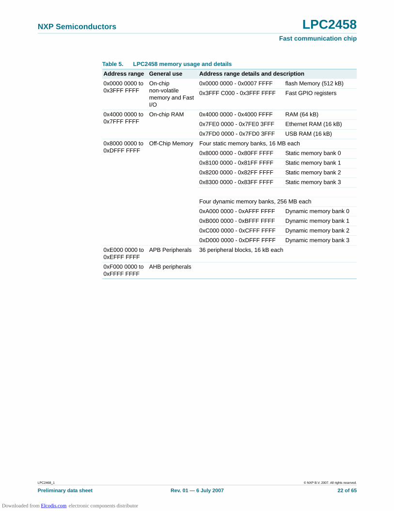
7.4 Memory mapThe LPC2458 memory map incorporates several distinct regions as shown in Table 5 and Figure 3.
In addition, the CPU interrupt vectors may be remapped to allow them to reside in either flash memory (default), boot ROM, or SRAM (see Section 7.26.6).
Downloaded from Elcodis.com electronic components distributor
LPC2468_1 © NXP B.V. 2007. All rights reserved.
Prelim inary da ta sheet Rev. 01 — 6 July 2007 22 of 65
NXP Semiconductors LPC2458Fast communica tion ch ip
Table 5. LPC2458 memor y usage and details
Address range General use Address range details an d descr ip tio n
0x0000 0000 to 0x3FFF FFFF
On-chip non-volatile memory and Fast I/O
0x0000 0000 - 0x0007 FFFF flash Memory (512 kB)
0x3FFF C000 - 0x3FFF FFFF Fast GPIO registers
0x4000 0000 to 0x7FFF FFFF
On-chip RAM 0x4000 0000 - 0x4000 FFFF RAM (64 kB)
0x7FE0 0000 - 0x7FE0 3FFF Ethernet RAM (16 kB)
0x7FD0 0000 - 0x7FD0 3FFF USB RAM (16 kB)
0x8000 0000 to 0xDFFF FFFF
Off-Chip Memory Four static memory banks, 16 MB each
0x8000 0000 - 0x80FF FFFF Static memory bank 0
0x8100 0000 - 0x81FF FFFF Static memory bank 1
0x8200 0000 - 0x82FF FFFF Static memory bank 2
0x8300 0000 - 0x83FF FFFF Static memory bank 3
Four dynamic memory banks, 256 MB each
0xA000 0000 - 0xAFFF FFFF Dynamic memory bank 0
0xB000 0000 - 0xBFFF FFFF Dynamic memory bank 1
0xC000 0000 - 0xCFFF FFFF Dynamic memory bank 2
0xD000 0000 - 0xDFFF FFFF Dynamic memory bank 3
0xE000 0000 to 0xEFFF FFFF
APB Peripherals 36 peripheral blocks, 16 kB each
0xF000 0000 to 0xFFFF FFFF
AHB peripherals
Downloaded from Elcodis.com electronic components distributor

LPC2468_1 © NXP B.V. 2007. All rights reserved.
Prelim inary da ta sheet Rev. 01 — 6 July 2007 23 of 65
NXP Semiconductors LPC2458Fast communica tion ch ip
7.5 Interrupt con trollerThe ARM processor core has two interrupt inputs called Interrupt Request (IRQ) and Fast Interrupt Request (FIQ). The VIC takes 32 interrupt request inputs which can be programmed as FIQ or vectored IRQ types. The programmable assignment scheme means that priorities of interrupts from the various peripherals can be dynamically assigned and adjusted.
FIQs have the highest priority. If more than one request is assigned to FIQ, the VIC ORs the requests to produce the FIQ signal to the ARM processor. The fastest possible FIQ latency is achieved when only one request is classified as FIQ, because then the FIQ
Fig 3. LPC2458 memory map
0.0 GB
1.0 GB
ON-CHIP NON-VOLATILE MEMORY
0x0000 0000
RESERVED ADDRESS SPACE
SPECIAL REGISTERS
ON-CHIP STATIC RAM
RESERVED ADDRESS SPACE
0x4000 0000
0x3FFF 8000
0x3FFF FFFF
2.0 GB 0x8000 0000
0x7FFF FFFFBOOT ROM AND BOOT FLASH
(BOOT FLASH REMAPPED FROM ON-CHIP FLASH)
3.0 GB 0xC000 0000
0xDFFF FFFF
RESERVED ADDRESS SPACE
EXTERNAL STATIC AND DYNAMIC MEMORY
3.75 GB
4.0 GB
3.5 GB
AHB PERIPHERALS
APB PERIPHERALS
0xE000 0000
0xF000 0000
0xFFFF FFFF
002aac736
Downloaded from Elcodis.com electronic components distributor

LPC2468_1 © NXP B.V. 2007. All rights reserved.
Prelim inary da ta sheet Rev. 01 — 6 July 2007 24 of 65
NXP Semiconductors LPC2458Fast communica tion ch ip
service routine can simply start dealing with that device. But if more than one request is assigned to the FIQ class, the FIQ service routine can read a word from the VIC that identifies which FIQ source(s) is (are) requesting an interrupt.
Vectored IRQs, which include all interrupt requests that are not classified as FIQs, have a programmable interrupt priority. When more than one interrupt is assigned the same priority and occur simultaneously, the one connected to the lowest numbered VIC channel will be serviced first.
The VIC ORs the requests from all of the vectored IRQs to produce the IRQ signal to the ARM processor. The IRQ service routine can start by reading a register from the VIC and jumping to the address supplied by that register.
7.5.1 Interrupt s ources
Each peripheral device has one interrupt line connected to the VIC but may have several interrupt flags. Individual interrupt flags may also represent more than one interrupt source.
Any pin on PORT0 and PORT2 (total of 64 pins) regardless of the selected function, can be programmed to generate an interrupt on a rising edge, a falling edge, or both. Such interrupt request coming from PORT0 and/or PORT2 will be combined with the EINT3 interrupt requests.
7.6 Pin connect b lockThe pin connect block allows selected pins of the microcontroller to have more than one function. Configuration registers control the multiplexers to allow connection between the pin and the on chip peripherals.
Peripherals should be connected to the appropriate pins prior to being activated and prior to any related interrupt(s) being enabled. Activity of any enabled peripheral function that is not mapped to a related pin should be considered undefined.
7.7 External memory controllerThe LPC2458 EMC is an ARM PrimeCell MultiPort Memory Controller peripheral offering support for asynchronous static memory devices such as RAM, ROM, and flash. In addition, it can be used as an interface with off-chip memory-mapped devices and peripherals. The EMC is an Advanced Microcontroller Bus Architecture (AMBA) compliant peripheral.
7.7.1 Features
• Dynamic memory interface support including Single Data Rate SDRAM
• Asynchronous static memory device support including RAM, ROM, and flash, with or without asynchronous page mode
• Low transaction latency
• Read and write buffers to reduce latency and to improve performance
• 8/16 data and 20 address lines wide static memory support
• 16 bit wide chip select SDRAM memory support
• Static memory features include:
Downloaded from Elcodis.com electronic components distributor
LPC2468_1 © NXP B.V. 2007. All rights reserved.
Prelim inary da ta sheet Rev. 01 — 6 July 2007 25 of 65
NXP Semiconductors LPC2458Fast communica tion ch ip
– Asynchronous page mode read
– Programmable Wait States
– Bus turnaround delay
– Output enable and write enable delays
– Extended wait
• Two chip selects for synchronous memory and two chip selects for static memory devices
• Power-saving modes dynamically control CKE and CLKOUT to SDRAMs
• Dynamic memory self-refresh mode controlled by software
• Controller supports 2 k, 4 k, and 8 k row address synchronous memory parts. That is typical 512 MB, 256 MB, and 128 MB parts, with 4, 8, 16, or 32 data bits per device
• Separate reset domains allow the for auto-refresh through a chip reset if desired
Note: Synchronous static memory devices (synchronous burst mode) are not supported.
7.8 General purpose DMA controllerThe GPDMA is an AMBA AHB compliant peripheral allowing selected LPC2458 peripherals to have DMA support.
The GPDMA enables peripheral-to-memory, memory-to-peripheral, peripheral-to-peripheral, and memory-to-memory transactions. Each DMA stream provides unidirectional serial DMA transfers for a single source and destination. For example, a bidirectional port requires one stream for transmit and one for receive. The source and destination areas can each be either a memory region or a peripheral, and can be accessed through the AHB master.
7.8.1 Features
• Two DMA channels. Each channel can support a unidirectional transfer.
• The GPDMA can transfer data between the 16 kB SRAM, external memory, and peripherals such as the SD/MMC, two SSPs, and the I2S interface.
• Single DMA and burst DMA request signals. Each peripheral connected to the GPDMA can assert either a burst DMA request or a single DMA request. The DMA burst size is set by programming the GPDMA.
• Memory-to-memory, memory-to-peripheral, peripheral-to-memory, and peripheral-to-peripheral transfers.
• Scatter or gather DMA is supported through the use of linked lists. This means that the source and destination areas do not have to occupy contiguous areas of memory.
• Hardware DMA channel priority. Each DMA channel has a specific hardware priority. DMA channel 0 has the highest priority and channel 1 has the lowest priority. If requests from two channels become active at the same time, the channel with the highest priority is serviced first.
• AHB slave DMA programming interface. The GPDMA is programmed by writing to the DMA control registers over the AHB slave interface.
• One AHB bus master for transferring data. This interface transfers data when a DMA request goes active.
Downloaded from Elcodis.com electronic components distributor

LPC2468_1 © NXP B.V. 2007. All rights reserved.
Prelim inary da ta sheet Rev. 01 — 6 July 2007 26 of 65
NXP Semiconductors LPC2458Fast communica tion ch ip
• 32-bit AHB master bus width.
• Incrementing or non-incrementing addressing for source and destination.
• Programmable DMA burst size. The DMA burst size can be programmed to more efficiently transfer data. Usually the burst size is set to half the size of the FIFO in the peripheral.
• Internal four-word FIFO per channel.
• Supports 8-bit, 16-bit, and 32-bit wide transactions.
• An interrupt to the processor can be generated on a DMA completion or when a DMA error has occurred.
• Interrupt masking. The DMA error and DMA terminal count interrupt requests can be masked.
• Raw interrupt status. The DMA error and DMA count raw interrupt status can be read prior to masking.
7.9 Fast general purpose p arallel I/ODevice pins that are not connected to a specific peripheral function are controlled by the GPIO registers. Pins may be dynamically configured as inputs or outputs. Separate registers allow setting or clearing any number of outputs simultaneously. The value of the output register may be read back as well as the current state of the port pins.
LPC2458 use accelerated GPIO functions:
• GPIO registers are relocated to the ARM local bus so that the fastest possible I/O timing can be achieved.
• Mask registers allow treating sets of port bits as a group, leaving other bits unchanged.
• All GPIO registers are byte and half-word addressable.
• Entire port value can be written in one instruction.
Additionally, any pin on PORT0 and PORT2 (total of 64 pins) that is not configured as an analog input/output can be programmed to generate an interrupt on a rising edge, a falling edge, or both. The edge detection is asynchronous, so it may operate when clocks are not present such as during Power-down mode. Each enabled interrupt can be used to wake the chip up from Power-down mode.
7.9.1 Features
• Bit level set and clear registers allow a single instruction to set or clear any number of bits in one port.
• Direction control of individual bits.
• All I/O default to inputs after reset.
• Backward compatibility with other earlier devices is maintained with legacy PORT0 and PORT1 registers appearing at the original addresses on the APB bus.
Downloaded from Elcodis.com electronic components distributor

LPC2468_1 © NXP B.V. 2007. All rights reserved.
Prelim inary da ta sheet Rev. 01 — 6 July 2007 27 of 65
NXP Semiconductors LPC2458Fast communica tion ch ip
7.10 EthernetThe Ethernet block contains a full featured 10 Mbit/s or 100 Mbit/s Ethernet MAC designed to provide optimized performance through the use of DMA hardware acceleration. Features include a generous suite of control registers, half or full duplex operation, flow control, control frames, hardware acceleration for transmit retry, receive packet filtering and wake-up on LAN activity. Automatic frame transmission and reception with scatter-gather DMA off-loads many operations from the CPU.
The Ethernet block and the CPU share a dedicated AHB subsystem that is used to access the Ethernet SRAM for Ethernet data, control, and status information. All other AHB traffic in the LPC2458 takes place on a different AHB subsystem, effectively separating Ethernet activity from the rest of the system. The Ethernet DMA can also access off-chip memory via the EMC, as well as the SRAM located on another AHB. However, using memory other than the Ethernet SRAM, especially off-chip memory, will slow Ethernet access to memory and increase the loading of its AHB.
The Ethernet block interfaces between an off-chip Ethernet PHY using the Media Independent Interface (MII) or Reduced MII (RMII) protocol and the on-chip Media Independent Interface Management (MIIM) serial bus.
7.10.1 Features
• Ethernet standards support:
– Supports 10 Mbit/s or 100 Mbit/s PHY devices including 10 Base-T, 100 Base-TX, 100 Base-FX, and 100 Base-T4.
– Fully compliant with IEEE standard 802.3.
– Fully compliant with 802.3x Full Duplex Flow Control and Half Duplex back pressure.
– Flexible transmit and receive frame options.
– Virtual Local Area Network (VLAN) frame support.
• Memory management:
– Independent transmit and receive buffers memory mapped to shared SRAM.
– DMA managers with scatter/gather DMA and arrays of frame descriptors.
– Memory traffic optimized by buffering and pre-fetching.
• Enhanced Ethernet features:
– Receive filtering.
– Multicast and broadcast frame support for both transmit and receive.
– Optional automatic Frame Check Sequence (FCS) insertion with Circular Redundancy Check (CRC) for transmit.
– Selectable automatic transmit frame padding.
– Over-length frame support for both transmit and receive allows any length frames.
– Promiscuous receive mode.
– Automatic collision back-off and frame retransmission.
– Includes power management by clock switching.
Downloaded from Elcodis.com electronic components distributor

LPC2468_1 © NXP B.V. 2007. All rights reserved.
Prelim inary da ta sheet Rev. 01 — 6 July 2007 28 of 65
NXP Semiconductors LPC2458Fast communica tion ch ip
– Wake-on-LAN power management support allows system wake-up: using the receive filters or a magic frame detection filter.
• Physical interface:
– Attachment of external PHY chip through standard MII or RMII interface.
– PHY register access is available via the MIIM interface.
7.11 USB interfaceThe Universal Serial Bus (USB) is a 4-wire bus that supports communication between a host and one or more (up to 127) peripherals. The Host Controller allocates the USB bandwidth to attached devices through a token-based protocol. The bus supports hot plugging and dynamic configuration of the devices. All transactions are initiated by the Host Controller.
The LPC2458 USB interface includes a Device, Host, and OTG Controller. Details on typical USB interfacing solutions can be found in Section 11.1 “Suggested USB interface solutions” on page 55
7.11.1 USB Device Controll er
The Device Controller enables 12 Mbit/s data exchange with a USB Host Controller. It consists of a register interface, serial interface engine, endpoint buffer memory, and a DMA controller. The serial interface engine decodes the USB data stream and writes data to the appropriate endpoint buffer. The status of a completed USB transfer or error condition is indicated via status registers. An interrupt is also generated if enabled. When enabled, the DMA controller transfers data between the endpoint buffer and the USB RAM.
7.11.1.1 Features
• Fully compliant with USB 2.0 specification (full speed).
• Supports 32 physical (16 logical) endpoints with a 4 kB endpoint buffer RAM.
• Supports Control, Bulk, Interrupt and Isochronous endpoints.
• Scalable realization of endpoints at run time.
• Endpoint Maximum packet size selection (up to USB maximum specification) by software at run time.
• Supports SoftConnect and GoodLink features.
• While USB is in the Suspend mode, LPC2458 can enter one of the reduced power modes and wake up on USB activity.
• Supports DMA transfers with the DMA RAM of 16 kB on all non-control endpoints.
• Allows dynamic switching between CPU-controlled and DMA modes.
• Double buffer implementation for Bulk and Isochronous endpoints.
7.11.2 USB Host Controller
The Host Controller enables full- and low-speed data exchange with USB devices attached to the bus. It consists of register interface, serial interface engine and DMA controller. The register interface complies with the OHCI specification.
Downloaded from Elcodis.com electronic components distributor

LPC2468_1 © NXP B.V. 2007. All rights reserved.
Prelim inary da ta sheet Rev. 01 — 6 July 2007 29 of 65
NXP Semiconductors LPC2458Fast communica tion ch ip
7.11.2.1 Features
• OHCI compliant.
• Two downstream ports.
• Supports per-port power switching.
7.11.3 USB OTG Controller
USB OTG (On-The-Go) is a supplement to the USB 2.0 specification that augments the capability of existing mobile devices and USB peripherals by adding host functionality for connection to USB peripherals.
The OTG Controller integrates the Host Controller, device controller, and a master-only I2C interface to implement OTG dual-role device functionality. The dedicated I2C interface controls an external OTG transceiver.
7.11.3.1 Features
• Fully compliant with On-The-Go supplement to the USB 2.0 Specification, Revision 1.0a.
• Hardware support for Host Negotiation Protocol (HNP).
• Includes a programmable timer required for HNP and Session Request Protocol (SRP).
• Supports any OTG transceiver compliant with the OTG Transceiver Specification (CEA-2011), Rev. 1.0.
7.12 CAN controller and accep tance filtersThe Controller Area Network (CAN) is a serial communications protocol which efficiently supports distributed real-time control with a very high level of security. Its domain of application ranges from high-speed networks to low cost multiplex wiring.
The CAN block is intended to support multiple CAN buses simultaneously, allowing the device to be used as a gateway, switch, or router between two of CAN buses in industrial or automotive applications.
Each CAN controller has a register structure similar to the NXP SJA1000 and the PeliCAN Library block, but the 8-bit registers of those devices have been combined in 32-bit words to allow simultaneous access in the ARM environment. The main operational difference is that the recognition of received Identifiers, known in CAN terminology as Acceptance Filtering, has been removed from the CAN controllers and centralized in a global Acceptance Filter.
7.12.1 Features
• Two CAN controllers and buses.
• Data rates to 1 Mbit/s on each bus.
• 32-bit register and RAM access.
• Compatible with CAN specification 2.0B, ISO 11898-1.
• Global Acceptance Filter recognizes 11-bit and 29-bit receive identifiers for all CAN buses.
Downloaded from Elcodis.com electronic components distributor

LPC2468_1 © NXP B.V. 2007. All rights reserved.
Prelim inary da ta sheet Rev. 01 — 6 July 2007 30 of 65
NXP Semiconductors LPC2458Fast communica tion ch ip
• Acceptance Filter can provide FullCAN-style automatic reception for selected Standard Identifiers.
• Full CAN messages can generate interrupts.
7.13 10-bit ADCThe LPC2458 contains one ADC. It is a single 10-bit successive approximation ADC with eight channels.
7.13.1 Features
• 10-bit successive approximation ADC
• Input multiplexing among 8 pins
• Power-down mode
• Measurement range 0 V to Vi(VREF)
• 10-bit conversion time t 2.44 Ps
• Burst conversion mode for single or multiple inputs
• Optional conversion on transition of input pin or Timer Match signal
• Individual result registers for each ADC channel to reduce interrupt overhead
7.14 10-bit DACThe DAC allows the LPC2458 to generate a variable analog output. The maximum output value of the DAC is Vi(VREF).
7.14.1 Features
• 10-bit DAC
• Resistor string architecture
• Buffered output
• Power-down mode
• Selectable output drive
7.15 UARTsThe LPC2458 contains four UARTs. In addition to standard transmit and receive data lines, UART1 also provides a full modem control handshake interface.
The UARTs include a fractional baud rate generator. Standard baud rates such as 115200 can be achieved with any crystal frequency above 2 MHz.
7.15.1 Features
• 16 B Receive and Transmit FIFOs.
• Register locations conform to 16C550 industry standard.
• Receiver FIFO trigger points at 1 B, 4 B, 8 B, and 14 B.
• Built-in fractional baud rate generator covering wide range of baud rates without a need for external crystals of particular values.
Downloaded from Elcodis.com electronic components distributor

LPC2468_1 © NXP B.V. 2007. All rights reserved.
Prelim inary da ta sheet Rev. 01 — 6 July 2007 31 of 65
NXP Semiconductors LPC2458Fast communica tion ch ip
• Fractional divider for baud rate control, auto baud capabilities and FIFO control mechanism that enables software flow control implementation.
• UART1 equipped with standard modem interface signals. This module also provides full support for hardware flow control (auto-CTS/RTS).
• UART3 includes an IrDA mode to support infrared communication.
7.16 SPI serial I/O controllerThe LPC2458 contains one SPI controller. SPI is a full duplex serial interface designed to handle multiple masters and slaves connected to a given bus. Only a single master and a single slave can communicate on the interface during a given data transfer. During a data transfer the master always sends 8 bits to 16 bits of data to the slave, and the slave always sends 8 bits to 16 bits of data to the master.
7.16.1 Features
• Compliant with SPI specification
• Synchronous, Serial, Full Duplex Communication
• Combined SPI master and slave
• Maximum data bit rate of one eighth of the input clock rate
• 8 bits to 16 bits per transfer
7.17 SSP serial I/O controllerThe LPC2458 contains two SSP controllers. The SSP controller is capable of operation on a SPI, 4-wire SSI, or Microwire bus. It can interact with multiple masters and slaves on the bus. Only a single master and a single slave can communicate on the bus during a given data transfer. The SSP supports full duplex transfers, with frames of 4 bits to 16 bits of data flowing from the master to the slave and from the slave to the master. In practice, often only one of these data flows carries meaningful data.
7.17.1 Features
• Compatible with Motorola SPI, 4-wire TI SSI, and National Semiconductor Microwire buses
• Synchronous serial communication
• Master or slave operation
• 8-frame FIFOs for both transmit and receive
• 4-bit to 16-bit frame
• Maximum SPI bus data bit rate of one half (Master mode) and one twelfth (Slave mode) of the input clock rate
• DMA transfers supported by GPDMA
7.18 SD/MMC card interfaceThe Secure Digital and Multimedia Card Interface (MCI) allows access to external SD memory cards. The SD card interface conforms to the SD Multimedia Card Specification Version 2.11.
Downloaded from Elcodis.com electronic components distributor

LPC2468_1 © NXP B.V. 2007. All rights reserved.
Prelim inary da ta sheet Rev. 01 — 6 July 2007 32 of 65
NXP Semiconductors LPC2458Fast communica tion ch ip
7.18.1 Features
• The MCI interface provides all functions specific to the SD/MMC memory card. These include the clock generation unit, power management control, and command and data transfer.
• Conforms to Multimedia Card Specification v2.11.
• Conforms to Secure Digital Memory Card Physical Layer Specification, v0.96.
• Can be used as a multimedia card bus or a secure digital memory card bus host. The SD/MMC can be connected to several multimedia cards or a single secure digital memory card.
• DMA supported through the GPDMA controller.
7.19 I2C-bus serial I/O contr ollerThe LPC2458 contains three I2C-bus controllers.
The I2C-bus is bidirectional, for inter-IC control using only two wires: a serial clock line (SCL), and a serial data line (SDA). Each device is recognized by a unique address and can operate as either a receiver-only device (e.g., an LCD driver) or a transmitter with the capability to both receive and send information (such as memory). Transmitters and/or receivers can operate in either master or slave mode, depending on whether the chip has to initiate a data transfer or is only addressed. The I2C-bus is a multi-master bus and can be controlled by more than one bus master connected to it.
The I2C-bus implemented in LPC2458 supports bit rates up to 400 kbit/s (Fast I2C-bus).
7.19.1 Features
• I2C0 is a standard I2C compliant bus interface with open-drain pins.
• I2C1 and I2C2 use standard I/O pins and do not support powering off of individual devices connected to the same bus lines.
• Easy to configure as master, slave, or master/slave.
• Programmable clocks allow versatile rate control.
• Bidirectional data transfer between masters and slaves.
• Multi-master bus (no central master).
• Arbitration between simultaneously transmitting masters without corruption of serial data on the bus.
• Serial clock synchronization allows devices with different bit rates to communicate via one serial bus.
• Serial clock synchronization can be used as a handshake mechanism to suspend and resume serial transfer.
• The I2C-bus can be used for test and diagnostic purposes.
7.20 I2S-bus serial I/O contro llersThe I2S-bus provides a standard communication interface for digital audio applications.
Downloaded from Elcodis.com electronic components distributor
LPC2468_1 © NXP B.V. 2007. All rights reserved.
Prelim inary da ta sheet Rev. 01 — 6 July 2007 33 of 65
NXP Semiconductors LPC2458Fast communica tion ch ip
The I2S-bus specification defines a 3-wire serial bus using one data line, one clock line, and one word select signal. The basic I2S connection has one master, which is always the master, and one slave. The I2S interface on the LPC2458 provides a separate transmit and receive channel, each of which can operate as either a master or a slave.
7.20.1 Features
• The interface has separate input/output channels each of which can operate in master or slave mode.
• Capable of handling 8-bit, 16-bit, and 32-bit word sizes.
• Mono and stereo audio data supported.
• The sampling frequency can range from 16 kHz to 48 kHz (16, 22.05, 32, 44.1, 48) kHz.
• Configurable word select period in master mode (separately for I2S input and output).
• Two 8 word FIFO data buffers are provided, one for transmit and one for receive.
• Generates interrupt requests when buffer levels cross a programmable boundary.
• Two DMA requests, controlled by programmable buffer levels. These are connected to the GPDMA block.
• Controls include reset, stop and mute options separately for I2S input and I2S output.
7.21 General purpose 32-bit time rs/external event coun tersThe LPC2458 includes four 32-bit Timer/Counters. The Timer/Counter is designed to count cycles of the system derived clock or an externally-supplied clock. It can optionally generate interrupts or perform other actions at specified timer values, based on four match registers. The Timer/Counter also includes four capture inputs to trap the timer value when an input signal transitions, optionally generating an interrupt.
7.21.1 Features
• A 32-bit Timer/Counter with a programmable 32-bit prescaler.
• Counter or Timer operation.
• Up to four 32-bit capture channels per timer, that can take a snapshot of the timer value when an input signal transitions. A capture event may also optionally generate an interrupt.
• Four 32-bit match registers that allow:
– Continuous operation with optional interrupt generation on match.
– Stop timer on match with optional interrupt generation.
– Reset timer on match with optional interrupt generation.
• Up to four external outputs corresponding to match registers, with the following capabilities:
– Set LOW on match.
– Set HIGH on match.
– Toggle on match.
– Do nothing on match.
Downloaded from Elcodis.com electronic components distributor
LPC2468_1 © NXP B.V. 2007. All rights reserved.
Prelim inary da ta sheet Rev. 01 — 6 July 2007 34 of 65
NXP Semiconductors LPC2458Fast communica tion ch ip
7.22 Pulse wid th mo dulatorThe PWM is based on the standard Timer block and inherits all of its features, although only the PWM function is pinned out on the LPC2458. The Timer is designed to count cycles of the system derived clock and optionally switch pins, generate interrupts or perform other actions when specified timer values occur, based on seven match registers. The PWM function is in addition to these features and is based on match register events.
The ability to separately control rising and falling edge locations allows the PWM to be used for more applications. For instance, multi-phase motor control typically requires three non-overlapping PWM outputs with individual control of all three pulse widths and positions.
Two match registers can be used to provide a single edge controlled PWM output. A dedicated match register controls the PWM cycle rate, by resetting the count upon match. The other match register controls the PWM edge position. Additional single edge controlled PWM outputs require only one match register each, since the repetition rate is the same for all PWM outputs. Multiple single edge controlled PWM outputs will all have a rising edge at the beginning of each PWM cycle, when an PWMMR0 match occurs.
Three match registers can be used to provide a PWM output with both edges controlled. Again, a dedicated match register controls the PWM cycle rate. The other match registers control the two PWM edge positions. Additional double edge controlled PWM outputs require only two match registers each, since the repetition rate is the same for all PWM outputs.
With double edge controlled PWM outputs, specific match registers control the rising and falling edge of the output. This allows both positive going PWM pulses (when the rising edge occurs prior to the falling edge), and negative going PWM pulses (when the falling edge occurs prior to the rising edge).
7.22.1 Features
• LPC2458 has two PWMs with the same operational features. These may be operated in a synchronized fashion by setting them both up to run at the same rate, then enabling both simultaneously. PWM0 acts as the master and PWM1 as the slave for this use.
• Counter or Timer operation (may use the peripheral clock or one of the capture inputs as the clock source).
• Seven match registers allow up to 6 single edge controlled or 3 double edge controlled PWM outputs, or a mix of both types. The match registers also allow:
– Continuous operation with optional interrupt generation on match.
– Stop timer on match with optional interrupt generation.
– Reset timer on match with optional interrupt generation.
• Supports single edge controlled and/or double edge controlled PWM outputs. Single edge controlled PWM outputs all go high at the beginning of each cycle unless the output is a constant low. Double edge controlled PWM outputs can have either edge occur at any position within a cycle. This allows for both positive going and negative going pulses.
Downloaded from Elcodis.com electronic components distributor

LPC2468_1 © NXP B.V. 2007. All rights reserved.
Prelim inary da ta sheet Rev. 01 — 6 July 2007 35 of 65
NXP Semiconductors LPC2458Fast communica tion ch ip
• Pulse period and width can be any number of timer counts. This allows complete flexibility in the trade-off between resolution and repetition rate. All PWM outputs will occur at the same repetition rate.
• Double edge controlled PWM outputs can be programmed to be either positive going or negative going pulses.
• Match register updates are synchronized with pulse outputs to prevent generation of erroneous pulses. Software must ‘release’ new match values before they can become effective.
• May be used as a standard timer if the PWM mode is not enabled.
• A 32-bit Timer/Counter with a programmable 32-bit Prescaler.
7.23 Watchdog timer (WDT)The purpose of the watchdog is to reset the microcontroller within a reasonable amount of time if it enters an erroneous state. When enabled, the watchdog will generate a system reset if the user program fails to ‘feed’ (or reload) the watchdog within a predetermined amount of time.
7.23.1 Features
• Internally resets chip if not periodically reloaded.
• Debug mode.
• Enabled by software but requires a hardware reset or a watchdog reset/interrupt to be disabled.
• Incorrect/Incomplete feed sequence causes reset/interrupt if enabled.
• Flag to indicate watchdog reset.
• Programmable 32-bit timer with internal prescaler.
• Selectable time period from (Tcy(WDCLK) u 256 u 4) to (Tcy(WDCLK) u 232 u 4) in multiples of Tcy(WDCLK) u 4.
• The Watchdog Clock (WDCLK) source can be selected from the RTC clock, the Internal RC oscillator (IRC), or the APB peripheral clock. This gives a wide range of potential timing choices of Watchdog operation under different power reduction conditions. It also provides the ability to run the WDT from an entirely internal source that is not dependent on an external crystal and its associated components and wiring, for increased reliability.
7.24 RTC and battery RAMThe RTC is a set of counters for measuring time when system power is on, and optionally when it is off. It uses little power in Power-down mode. On the LPC2458, the RTC can be clocked by a separate 32.768 kHz oscillator or by a programmable prescale divider based on the APB clock. Also, the RTC is powered by its own power supply pin, VBAT, which can be connected to a battery or to the same 3.3 V supply used by the rest of the device.
The VBAT pin supplies power only to the RTC and the Battery RAM. These two functions require a minimum of power to operate, which can be supplied by an external battery. When the CPU and the rest of chip functions are stopped and power removed, the RTC can supply an alarm output that can be used by external hardware to restore chip power and resume operation.
Downloaded from Elcodis.com electronic components distributor

LPC2468_1 © NXP B.V. 2007. All rights reserved.
Prelim inary da ta sheet Rev. 01 — 6 July 2007 36 of 65
NXP Semiconductors LPC2458Fast communica tion ch ip
7.24.1 Features
• Measures the passage of time to maintain a calendar and clock.
• Ultra low power design to support battery powered systems.
• Provides Seconds, Minutes, Hours, Day of Month, Month, Year, Day of Week, and Day of Year.
• Dedicated 32 kHz oscillator or programmable prescaler from APB clock.
• Dedicated power supply pin can be connected to a battery or to the main 3.3 V.
• An alarm output pin is included to assist in waking up when the chip has had power removed to all functions except the RTC and Battery RAM.
• Periodic interrupts can be generated from increments of any field of the time registers, and selected fractional second values. This enhancement enables the RTC to be used as a System Timer.
• 2 kB data SRAM powered by VBAT.
• RTC and Battery RAM power supply is isolated from the rest of the chip.
7.25 Clocking and power control
7.25.1 Cryst al oscilla tors
The LPC2458 includes three independent oscillators. These are the Main Oscillator, the Internal RC oscillator, and the RTC oscillator. Each oscillator can be used for more than one purpose as required in a particular application. Any of the three clock sources can be chosen by software to drive the PLL and ultimately the CPU.
Following reset, the LPC2458 will operate from the Internal RC oscillator until switched by software. This allows systems to operate without any external crystal and the bootloader code to operate at a known frequency.
7.25.1.1 Internal RC oscilla tor
The IRC may be used as the clock source for the WDT, and/or as the clock that drives the PLL and subsequently the CPU. The nominal IRC frequency is 4 MHz. The IRC is trimmed to 1 % accuracy.
Upon power-up or any chip reset, the LPC2458 uses the IRC as the clock source. Software may later switch to one of the other available clock sources.
7.25.1.2 Main o sci llator
The main oscillator can be used as the clock source for the CPU, with or without using the PLL. The main oscillator operates at frequencies of 1 MHz to 24 MHz. This frequency can be boosted to a higher frequency, up to the maximum CPU operating frequency, by the PLL. The clock selected as the PLL input is PLLCLKIN. The ARM processor clock frequency is referred to as CCLK elsewhere in this document. The frequencies of PLLCLKIN and CCLK are the same value unless the PLL is active and connected. The clock frequency for each peripheral can be selected individually and is referred to as PCLK. Refer to Section 7.25.2 for additional information.
Downloaded from Elcodis.com electronic components distributor
LPC2468_1 © NXP B.V. 2007. All rights reserved.
Prelim inary da ta sheet Rev. 01 — 6 July 2007 37 of 65
NXP Semiconductors LPC2458Fast communica tion ch ip
7.25.1.3 RTC oscillator
The RTC oscillator can be used as the clock source for the RTC and/or the WDT. Also, the RTC oscillator can be used to drive the PLL and the CPU.
7.25.2 PLL
The PLL accepts an input clock frequency in the range of 32 kHz to 50 MHz. The input frequency is multiplied up to a high frequency, then divided down to provide the actual clock used by the CPU and the USB block.
The PLL input, in the range of 32 kHZ to 50 MHz, may initially be divided down by a value ‘N’, which may be in the range of 1 to 256. This input division provides a wide range of output frequencies from the same input frequency.
Following the PLL input divider is the PLL multiplier. This can multiply the input divider output through the use of a Current Controlled Oscillator (CCO) by a value ‘M’, in the range of 1 through 32768. The resulting frequency must be in the range of 275 MHz to 550 MHz. The multiplier works by dividing the CCO output by the value of M, then using a phase-frequency detector to compare the divided CCO output to the multiplier input. The error value is used to adjust the CCO frequency.
The PLL is turned off and bypassed following a chip Reset and by entering Power-down mode. PLL is enabled by software only. The program must configure and activate the PLL, wait for the PLL to lock, then connect to the PLL as a clock source.
7.25.3 Wake-up time r
The LPC2458 begins operation at power-up and when awakened from Power-down mode by using the 4 MHz IRC oscillator as the clock source. This allows chip operation to resume quickly. If the main oscillator or the PLL is needed by the application, software will need to enable these features and wait for them to stabilize before they are used as a clock source.
When the main oscillator is initially activated, the wake-up timer allows software to ensure that the main oscillator is fully functional before the processor uses it as a clock source and starts to execute instructions. This is important at power on, all types of Reset, and whenever any of the aforementioned functions are turned off for any reason. Since the oscillator and other functions are turned off during Power-down mode, any wake-up of the processor from Power-down mode makes use of the wake-up Timer.
The Wake-up Timer monitors the crystal oscillator to check whether it is safe to begin code execution. When power is applied to the chip, or when some event caused the chip to exit Power-down mode, some time is required for the oscillator to produce a signal of sufficient amplitude to drive the clock logic. The amount of time depends on many factors, including the rate of VDD(3V3) ramp (in the case of power on), the type of crystal and its electrical characteristics (if a quartz crystal is used), as well as any other external circuitry (e.g., capacitors), and the characteristics of the oscillator itself under the existing ambient conditions.
7.25.4 Power control
The LPC2458 supports a variety of power control features. There are three special modes of processor power reduction: Idle mode, Sleep mode, and Power-down mode. The CPU clock rate may also be controlled as needed by changing clock sources, reconfiguring
Downloaded from Elcodis.com electronic components distributor

LPC2468_1 © NXP B.V. 2007. All rights reserved.
Prelim inary da ta sheet Rev. 01 — 6 July 2007 38 of 65
NXP Semiconductors LPC2458Fast communica tion ch ip
PLL values, and/or altering the CPU clock divider value. This allows a trade-off of power versus processing speed based on application requirements. In addition, Peripheral power control allows shutting down the clocks to individual on-chip peripherals, allowing fine tuning of power consumption by eliminating all dynamic power use in any peripherals that are not required for the application. Each of the peripherals has its own clock divider which provides even better power control.
The LPC2458 also implements a separate power domain in order to allow turning off power to the bulk of the device while maintaining operation of the RTC and a small SRAM, referred to as the Battery RAM.
7.25.4.1 Idle mode
In Idle mode, execution of instructions is suspended until either a Reset or interrupt occurs. Peripheral functions continue operation during Idle mode and may generate interrupts to cause the processor to resume execution. Idle mode eliminates dynamic power used by the processor itself, memory systems and related controllers, and internal buses.
7.25.4.2 Sleep mode
In Sleep mode, the oscillator is shut down and the chip receives no internal clocks. The processor state and registers, peripheral registers, and internal SRAM values are preserved throughout Sleep mode and the logic levels of chip pins remain static. The output of the IRC is disabled but the IRC is not powered down for a fast wake-up later. The 32 kHz RTC oscillator is not stopped because the RTC interrupts may be used as the wake-up source. The PLL is automatically turned off and disconnected. The CCLK and USB clock dividers automatically get reset to zero.
The Sleep mode can be terminated and normal operation resumed by either a Reset or certain specific interrupts that are able to function without clocks. Since all dynamic operation of the chip is suspended, Sleep mode reduces chip power consumption to a very low value. The flash memory is left on in Sleep mode, allowing a very quick wake-up.
On the wake-up from Sleep mode, if the IRC was used before entering Sleep mode, the code execution and peripherals activities will resume after 4 cycles expire. If the main external oscillator was used, the code execution will resume when 4096 cycles expire.
The customers need to reconfigure the PLL and clock dividers accordingly.
7.25.4.3 Power- down mo de
Power-down mode does everything that Sleep mode does, but also turns off the IRC oscillator and the flash memory. This saves more power, but requires waiting for resumption of flash operation before execution of code or data access in the flash memory can be accomplished.
On the wake-up from Power-down mode, if the IRC was used before entering Power-down mode, it will take IRC 60 Ps to start-up. After this 4 IRC cycles will expire before the code execution can then be resumed if the code was running from SRAM. In the meantime, the flash wake-up timer then counts 4 MHz IRC clock cycles to make the 100 Ps flash start-up time. When it times out, access to the flash will be allowed. The customers need to reconfigure the PLL and clock dividers accordingly.
Downloaded from Elcodis.com electronic components distributor

LPC2468_1 © NXP B.V. 2007. All rights reserved.
Prelim inary da ta sheet Rev. 01 — 6 July 2007 39 of 65
NXP Semiconductors LPC2458Fast communica tion ch ip
7.25.4.4 Power doma ins
The LPC2458 provides two independent power domains that allow the bulk of the device to have power removed while maintaining operation of the RTC and the Battery RAM.
On the LPC2458, I/O pads are powered by the 3.3 V (VDD(3V3)) pins, while the VDD(DCDC)(3V3) pins power the on-chip DC-to-DC converter which in turn provides power to the CPU and most of the peripherals.
Although both the I/O pad ring and the core require a 3.3 V supply, different powering schemes can be used depending on the actual application requirements.
The first option assumes that power consumption is not a concern and the design ties the VDD(3V3) and VDD(DCDC)(3V3) pins together. This approach requires only one 3.3 V power supply for both pads, the CPU, and peripherals. While this solution is simple, it does not support powering down the I/O pad ring “on the fly” while keeping the CPU and peripherals alive.
The second option uses two power supplies; a 3.3 V supply for the I/O pads (VDD(3V3)) and a dedicated 3.3 V supply for the CPU (VDD(DCDC)(3V3)). Having the on-chip DC-DC converter powered independently from the I/O pad ring enables shutting down of the I/O pad power supply “on the fly”, while the CPU and peripherals stay active.
The VBAT pin supplies power only to the RTC and the Battery RAM. These two functions require a minimum of power to operate, which can be supplied by an external battery. When the CPU and the rest of chip functions are stopped and power removed, the RTC can supply an alarm output that may be used by external hardware to restore chip power and resume operation.
7.26 System control
7.26.1 Reset
Reset has four sources on the LPC2458: the RESET pin, the Watchdog reset, power-on reset, and the BrownOut Detection (BOD) circuit. The RESET pin is a Schmitt trigger input pin. Assertion of chip Reset by any source, once the operating voltage attains a usable level, starts the Wake-up timer (see description in Section 7.25.3 “Wake-up timer”), causing reset to remain asserted until the external Reset is de-asserted, the oscillator is running, a fixed number of clocks have passed, and the flash controller has completed its initialization.
When the internal Reset is removed, the processor begins executing at address 0, which is initially the Reset vector mapped from the Boot Block. At that point, all of the processor and peripheral registers have been initialized to predetermined values.
7.26.2 Browno ut detec tion
The LPC2458 includes 2-stage monitoring of the voltage on the VDD(3V3) pins. If this voltage falls below 2.95 V, the BOD asserts an interrupt signal to the Vectored Interrupt Controller. This signal can be enabled for interrupt in the Interrupt Enable Register in the VIC in order to cause a CPU interrupt; if not, software can monitor the signal by reading a dedicated status register.
Downloaded from Elcodis.com electronic components distributor

LPC2468_1 © NXP B.V. 2007. All rights reserved.
Prelim inary da ta sheet Rev. 01 — 6 July 2007 40 of 65
NXP Semiconductors LPC2458Fast communica tion ch ip
The second stage of low-voltage detection asserts Reset to inactivate the LPC2458 when the voltage on the VDD(3V3) pins falls below 2.65 V. This Reset prevents alteration of the flash as operation of the various elements of the chip would otherwise become unreliable due to low voltage. The BOD circuit maintains this reset down below 1 V, at which point the power-on reset circuitry maintains the overall Reset.
Both the 2.95 V and 2.65 V thresholds include some hysteresis. In normal operation, this hysteresis allows the 2.95 V detection to reliably interrupt, or a regularly-executed event loop to sense the condition.
7.26.3 Code s ecurity (Code Read Protection - CRP)
This feature of the LPC2458 allows user to enable different levels of security in the system so that access to the on-chip flash and use of the JTAG and ISP can be restricted. When needed, CRP is invoked by programming a specific pattern into a dedicated flash location. IAP commands are not affected by the CRP.
There are three levels of the Code Read Protection.
CRP1 disables access to chip via the JTAG and allows partial flash update (excluding flash sector 0) using a limited set of the ISP commands. This mode is useful when CRP is required and flash field updates are needed but all sectors can not be erased.
CRP2 disables access to chip via the JTAG and only allows full flash erase and update using a reduced set of the ISP commands.
Running an application with level CRP3 selected fully disables any access to chip via the JTAG pins and the ISP. This mode effectively disables ISP overide using P2[10] pin, too. It is up to the user’s application to provide (if needed) flash update mechanism using IAP calls or call reinvoke ISP command to enable flash update via UART0.
7.26.4 AHB bus
The LPC2458 implements two AHB buses in order to allow the Ethernet block to operate without interference caused by other system activity. The primary AHB, referred to as AHB1, includes the Vectored Interrupt Controller, GPDMA controller, USB interface, and 16 kB SRAM.
The second AHB, referred to as AHB2, includes only the Ethernet block and an associated 16 kB SRAM. In addition, a bus bridge is provided that allows the secondary AHB to be a bus master on AHB1, allowing expansion of Ethernet buffer space into off-chip memory or unused space in memory residing on AHB1.
In summary, bus masters with access to AHB1 are the ARM7 itself, the USB block, the GPDMA function, and the Ethernet block (via the bus bridge from AHB2). Bus masters with access to AHB2 are the ARM7 and the Ethernet block.
CAUTION
If level three Code Read Protection (CRP3) is selected, no future factory testing can be performed on the device.
Downloaded from Elcodis.com electronic components distributor
LPC2468_1 © NXP B.V. 2007. All rights reserved.
Prelim inary da ta sheet Rev. 01 — 6 July 2007 41 of 65
NXP Semiconductors LPC2458Fast communica tion ch ip
7.26.5 External interrupt input s
The LPC2458 includes up to 68 edge sensitive interrupt inputs combined with up to four level sensitive external interrupt inputs as selectable pin functions. The external interrupt inputs can optionally be used to wake up the processor from Power-down mode.
7.26.6 Memory ma pping co ntro l
The memory mapping control alters the mapping of the interrupt vectors that appear at the beginning at address 0x0000 0000. Vectors may be mapped to the bottom of the Boot ROM, the SRAM, or external memory. This allows code running in different memory spaces to have control of the interrupts.
7.27 Emulation and debuggingThe LPC2458 support emulation and debugging via a JTAG serial port. A trace port allows tracing program execution. Debugging and trace functions are multiplexed only with GPIOs on P2[0] to P2[9]. This means that all communication, timer, and interface peripherals residing on other pins are available during the development and debugging phase as they are when the application is run in the embedded system itself.
7.27.1 EmbeddedICE
The EmbeddedICE logic provides on-chip debug support. The debugging of the target system requires a host computer running the debugger software and an EmbeddedICE protocol convertor. The EmbeddedICE protocol convertor converts the Remote Debug Protocol commands to the JTAG data needed to access the ARM7TDMI-S core present on the target system.
The ARM core has a Debug Communication Channel (DCC) function built-in. The DCC allows a program running on the target to communicate with the host debugger or another separate host without stopping the program flow or even entering the debug state. The DCC is accessed as a coprocessor 14 by the program running on the ARM7TDMI-S core. The DCC allows the JTAG port to be used for sending and receiving data without affecting the normal program flow. The DCC data and control registers are mapped in to addresses in the EmbeddedICE logic.
7.27.2 Embedded trace
Since the LPC2458 have significant amounts of on-chip memories, it is not possible to determine how the processor core is operating simply by observing the external pins. The ETM provides real-time trace capability for deeply embedded processor cores. It outputs information about processor execution to a trace port. A software debugger allows configuration of the ETM using a JTAG interface and displays the trace information that has been captured.
The ETM is connected directly to the ARM core and not to the main AMBA system bus. It compresses the trace information and exports it through a narrow trace port. An external Trace Port Analyzer captures the trace information under software debugger control. The trace port can broadcast the Instruction trace information. Instruction trace (or PC trace) shows the flow of execution of the processor and provides a list of all the instructions that were executed. Instruction trace is significantly compressed by only broadcasting branch addresses as well as a set of status signals that indicate the pipeline status on a cycle by cycle basis. Trace information generation can be controlled by selecting the trigger resource. Trigger resources include address comparators, counters and sequencers.
Downloaded from Elcodis.com electronic components distributor

LPC2468_1 © NXP B.V. 2007. All rights reserved.
Prelim inary da ta sheet Rev. 01 — 6 July 2007 42 of 65
NXP Semiconductors LPC2458Fast communica tion ch ip
Since trace information is compressed the software debugger requires a static image of the code being executed. Self-modifying code can not be traced because of this restriction.
7.27.3 RealMonitor
RealMonitor is a configurable software module, developed by ARM Inc., which enables real-time debug. It is a lightweight debug monitor that runs in the background while users debug their foreground application. It communicates with the host using the DCC, which is present in the EmbeddedICE logic. The LPC2458 contain a specific configuration of RealMonitor software programmed into the on-chip ROM memory.
Downloaded from Elcodis.com electronic components distributor
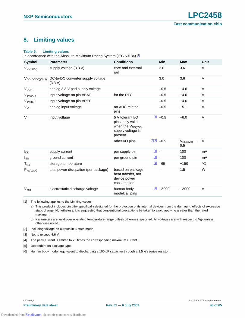
LPC2468_1 © NXP B.V. 2007. All rights reserved.
Prelim inary da ta sheet Rev. 01 — 6 July 2007 43 of 65
NXP Semiconductors LPC2458Fast communica tion ch ip
8. Limiting values
[1] The following applies to the Limiting values:
a) This product includes circuitry specifically designed for the protection of its internal devices from the damaging effects of excessive static charge. Nonetheless, it is suggested that conventional precautions be taken to avoid applying greater than the rated maximum.
b) Parameters are valid over operating temperature range unless otherwise specified. All voltages are with respect to VSS unless otherwise noted.
[2] Including voltage on outputs in 3-state mode.
[3] Not to exceed 4.6 V.
[4] The peak current is limited to 25 times the corresponding maximum current.
[5] Dependent on package type.
[6] Human body model: equivalent to discharging a 100 pF capacitor through a 1.5 k: series resistor.
Table 6. Limiting valuesIn accordance with the Absolute Maximum Rating System (IEC 60134).[1]
Symbol Parameter Conditio ns Min Max Unit
VDD(3V3) supply voltage (3.3 V) core and external rail
3.0 3.6 V
VDD(DCDC)(3V3) DC-to-DC converter supply voltage (3.3 V)
3.0 3.6 V
VDDA analog 3.3 V pad supply voltage �0.5 +4.6 V
Vi(VBAT) input voltage on pin VBAT for the RTC �0.5 +4.6 V
Vi(VREF) input voltage on pin VREF �0.5 +4.6 V
VIA analog input voltage on ADC related pins
�0.5 +5.1 V
VI input voltage 5 V tolerant I/O pins; only valid when the VDD(3V3) supply voltage is present
[2] �0.5 +6.0 V
other I/O pins [2][3] �0.5 VDD(3V3) + 0.5
V
IDD supply current per supply pin [4] - 100 mA
ISS ground current per ground pin [4] - 100 mA
Tstg storage temperature [5] �65 +150 qC
Ptot(pack) total power dissipation (per package) based on package heat transfer, not device power consumption
- 1.5 W
Vesd electrostatic discharge voltage human body model; all pins
[6] �2000 +2000 V
Downloaded from Elcodis.com electronic components distributor

LPC2468_1 © NXP B.V. 2007. All rights reserved.
Prelim inary da ta sheet Rev. 01 — 6 July 2007 44 of 65
NXP Semiconductors LPC2458Fast communica tion ch ip
9. Static characteristics
Table 7. Static ch aracteristicsTamb = �40 qC to +85 qC for commercial applications, unless otherwise specified.
Symbol Parameter Conditions Min Typ[1] Max Unit
VDD(3V3) supply voltage (3.3 V) core and external rail 3.0 3.3 3.6 V
VDD(DCDC)(3V3) DC-to-DC converter supply voltage (3.3 V)
3.0 3.3 3.6 V
VDDA analog 3.3 V pad supply voltage
3.0 3.3 3.6 V
Vi(VBAT) input voltage on pin VBAT
[2] 2.0 3.3 3.6 V
Vi(VREF) input voltage on pin VREF
2.5 3.3 VDDA V
Standard port pins, RESET , RTCK
IIL LOW-level input current
VI = 0 V; no pull-up - - 3 PA
IIH HIGH-level input current
VI = VDD(3V3); no pull-down - - 3 PA
IOZ OFF-state output current
VO = 0 V; VO = VDD(3V3); no pull-up/down
- - 3 PA
Ilatch I/O latch-up current �(0.5VDD(3V3)) < VI < (1.5VDD(3V3));
Tj < 125 qC
- - 100 mA
VI input voltage pin configured to provide a digital function
[3][4][5] 0 - 5.5 V
VO output voltage output active 0 - VDD(3V3) V
VIH HIGH-level input voltage
2.0 - - V
VIL LOW-level input voltage
- - 0.8 V
Vhys hysteresis voltage - 0.4 - V
VOH HIGH-level output voltage
IOH = �4 mA [6] VDD(3V3) � 0.4
- - V
VOL LOW-level output voltage
IOL = �4 mA [6] - - 0.4 V
IOH HIGH-level output current
VOH = VDD(3V3) � 0.4 V [6] �4 - - mA
IOL LOW-level output current
VOL = 0.4 V [6] 4 - - mA
IOHS HIGH-level short-circuit output current
VOH = 0 V [7] - - �45 mA
IOLS LOW-level short-circuit output current
VOL = VDDA[7] - - 50 mA
Ipd pull-down current VI = 5 V [8] 10 50 150 PA
Ipu pull-up current VI = 0 V �15 �50 �85 PA
VDD(3V3) < VI < 5 V [8] 0 0 0 PA
Downloaded from Elcodis.com electronic components distributor

LPC2468_1 © NXP B.V. 2007. All rights reserved.
Prelim inary da ta sheet Rev. 01 — 6 July 2007 45 of 65
NXP Semiconductors LPC2458Fast communica tion ch ip
IDD(DCDC)act(3V3) active mode DC-to-DC converter supply current (3.3 V)
VDD(DCDC)(3V3) = 3.3 V; Tamb = 25 qC; code
while(1){}
executed from flash; no peripherals enabled; PCLK = CCLK
CCLK = 10 MHz - 15 - mA
CCLK = 72 MHz - 63 - mA
all peripherals enabled; PCLK = CCLK / 8
CCLK = 10 MHz - 21 - mA
CCLK = 72 MHz - 92 - mA
all peripherals enabled; PCLK = CCLK
CCLK = 10 MHz - 27 - mA
CCLK = 72 MHz - 125 - mA
IDD(DCDC)pd(3V3) power-down mode DC-to-DC converter supply current (3.3 V)
VDD(DCDC)(3V3) = 3.3 V; Tamb = 25 qC
- 150 - PA
IBATact active mode battery supply current
DC-to-DC converter on [9] - 20 - PA
DC-to-DC converter off [9] - 28 - PA
I2C-bus pins (P0[27] and P0[28])
VIH HIGH-level input voltage
0.7VDD(3V3) - - V
VIL LOW-level input voltage
- - 0.3VDD(3V3) V
Vhys hysteresis voltage - 0.5VDD(3V) - V
VOL LOW-level output voltage
IOLS = 3 mA [6] - - 0.4 V
ILI input leakage current VI = VDD(3V3)[10] - 2 4 PA
VI = 5 V - 10 22 PA
Osci llator pins
Vi(XTAL1) input voltage on pin XTAL1
0 - 1.8 V
Vo(XTAL2) output voltage on pin XTAL2
0 - 1.8 V
Vi(RTCX1) input voltage on pin RTCX1
0 - 1.8 V
Vo(RTCX2) output voltage on pin RTCX2
0 - 1.8 V
USB pi ns
IOZ OFF-state output current
0 V < VI < 3.3 V - - r10 PA
VBUS bus supply voltage - - 5.25 V
Table 7. Static ch aracteristics …continuedTamb = �40 qC to +85 qC for commercial applications, unless otherwise specified.
Symbol Parameter Conditions Min Typ[1] Max Unit
Downloaded from Elcodis.com electronic components distributor

LPC2468_1 © NXP B.V. 2007. All rights reserved.
Prelim inary da ta sheet Rev. 01 — 6 July 2007 46 of 65
NXP Semiconductors LPC2458Fast communica tion ch ip
[1] Typical ratings are not guaranteed. The values listed are at room temperature (25 qC), nominal supply voltages
[2] The RTC typically fails when Vi(VBAT) drops below 1.6 V.
[3] Including voltage on outputs in 3-state mode.
[4] VDD(3V3) supply voltages must be present.
[5] 3-state outputs go into 3-state mode when VDD(3V3) is grounded.
[6] Accounts for 100 mV voltage drop in all supply lines.
[7] Only allowed for a short time period.
[8] Minimum condition for VI = 4.5 V, maximum condition for VI = 5.5 V.
[9] On pin VBAT.
[10] To VSS.
[11] Includes external resistors of 18 : r 1 % on D+ and D�.
VDI differential input sensitivity
_(D+) � (D�)_ 0.2 - - V
VCM differential common mode voltage range
includes VDI range 0.8 - 2.5 V
Vth(rs)se single-ended receiver switching threshold voltage
0.8 - 2.0 V
VOL LOW-level output voltage for low-/full-speed
RL of 1.5 k: to 3.6 V - - 0.18 V
VOH HIGH-level output voltage (driven) for low-/full-speed
RL of 15 k: to GND 2.8 - 3.5 V
Ctrans transceiver capacitance
pin to GND - - 20 pF
ZDRV driver output impedance for driver which is not high-speed capable
with 33 : series resistor; steady state drive
[11] 36 - 44.1 :
Rpu pull-up resistance SoftConnect = ON 1.1 - 1.9 k:
Table 7. Static ch aracteristics …continuedTamb = �40 qC to +85 qC for commercial applications, unless otherwise specified.
Symbol Parameter Conditions Min Typ[1] Max Unit
Table 8. ADC static ch aracteristicsVDDA = 2.5 V to 3.6 V; Tamb = �40 qC to +85 qC unless otherwise specified; ADC frequency 4.5 MHz.
Symbol Parameter Conditions Min Typ Max Unit
VIA analog input voltage 0 - VDDA V
Cia analog input capacitance - - 1 pF
ED differential linearity error [1][2][3] - - r1 LSB
EL(adj) integral non-linearity [1][4] - - r2 LSB
EO offset error [1][5] - - r3 LSB
EG gain error [1][6] - - r0.5 %
ET absolute error [1][7] - - r4 LSB
Rvsi voltage source interface resistance
[8] - - 40 k:
Downloaded from Elcodis.com electronic components distributor
LPC2468_1 © NXP B.V. 2007. All rights reserved.
Prelim inary da ta sheet Rev. 01 — 6 July 2007 47 of 65
NXP Semiconductors LPC2458Fast communica tion ch ip
[1] Conditions: VSSA = 0 V, VDDA = 3.3 V.
[2] The ADC is monotonic, there are no missing codes.
[3] The differential linearity error (ED) is the difference between the actual step width and the ideal step width. See Figure 4.
[4] The integral non-linearity (EL(adj)) is the peak difference between the center of the steps of the actual and the ideal transfer curve after appropriate adjustment of gain and offset errors. See Figure 4.
[5] The offset error (EO) is the absolute difference between the straight line which fits the actual curve and the straight line which fits the ideal curve. See Figure 4.
[6] The gain error (EG) is the relative difference in percent between the straight line fitting the actual transfer curve after removing offset error, and the straight line which fits the ideal transfer curve. See Figure 4.
[7] The absolute error (ET) is the maximum difference between the center of the steps of the actual transfer curve of the non-calibrated ADC and the ideal transfer curve. See Figure 4.
[8] See Figure 5.
Downloaded from Elcodis.com electronic components distributor
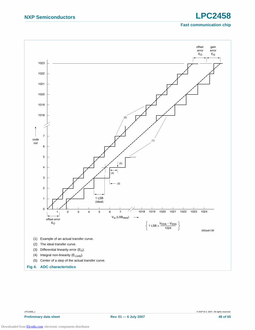
LPC2468_1 © NXP B.V. 2007. All rights reserved.
Prelim inary da ta sheet Rev. 01 — 6 July 2007 48 of 65
NXP Semiconductors LPC2458Fast communica tion ch ip
(1) Example of an actual transfer curve.
(2) The ideal transfer curve.
(3) Differential linearity error (ED).
(4) Integral non-linearity (EL(adj)).
(5) Center of a step of the actual transfer curve.
Fig 4. ADC characteristic s
002aab136
1023
1022
1021
1020
1019
(2)
(1)
10241018 1019 1020 1021 1022 102371 2 3 4 5 6
7
6
5
4
3
2
1
0
1018
(5)
(4)
(3)
1 LSB
(ideal)
code
out
VDDA − VSSA
1024
offset
error
EO
gain
error
EG
offset error
EO
Via (LSBideal)
1 LSB =
Downloaded from Elcodis.com electronic components distributor
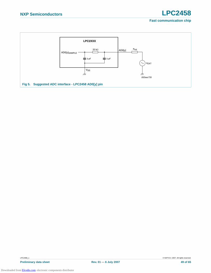
LPC2468_1 © NXP B.V. 2007. All rights reserved.
Prelim inary da ta sheet Rev. 01 — 6 July 2007 49 of 65
NXP Semiconductors LPC2458Fast communica tion ch ip
Fig 5. Sugges ted ADC inter face - LPC2458 AD0[y ] pin
LPC2XXX
AD0[y]SAMPLE
AD0[y]20 k:
3 pF 5 pF
Rvsi
VSS
VEXT
002aac733
Downloaded from Elcodis.com electronic components distributor
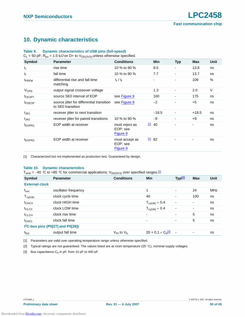
LPC2468_1 © NXP B.V. 2007. All rights reserved.
Prelim inary da ta sheet Rev. 01 — 6 July 2007 50 of 65
NXP Semiconductors LPC2458Fast communica tion ch ip
10. Dynamic characteristics
[1] Characterized but not implemented as production test. Guaranteed by design.
[1] Parameters are valid over operating temperature range unless otherwise specified.
[2] Typical ratings are not guaranteed. The values listed are at room temperature (25 qC), nominal supply voltages.
[3] Bus capacitance Cb in pF, from 10 pF to 400 pF.
Table 9. Dynamic character istics of USB pins (full-sp eed)CL = 50 pF; Rpu = 1.5 k: on D+ to VDD(3V3),unless otherwise specified.
Symbol Parameter Conditions Min Typ Max Unit
tr rise time 10 % to 90 % 8.5 - 13.8 ns
tf fall time 10 % to 90 % 7.7 - 13.7 ns
tFRFM differential rise and fall time matching
tr / tf - - 109 %
VCRS output signal crossover voltage 1.3 - 2.0 V
tFEOPT source SE0 interval of EOP see Figure 9 160 - 175 ns
tFDEOP source jitter for differential transition to SE0 transition
see Figure 9 �2 - +5 ns
tJR1 receiver jitter to next transition �18.5 - +18.5 ns
tJR2 receiver jitter for paired transitions 10 % to 90 % �9 - +9 ns
tEOPR1 EOP width at receiver must reject as EOP; see Figure 9
[1] 40 - - ns
tEOPR2 EOP width at receiver must accept as EOP; see Figure 9
[1] 82 - - ns
Table 10. Dynamic character isticsTamb = �40 qC to +85 qC for commercial applications; VDD(3V3) over specified ranges.[1]
Symbol Parameter Conditions Min Typ[2] Max Unit
Extern al clo ck
fosc oscillator frequency 1 - 24 MHz
Tcy(clk) clock cycle time 40 - 100 ns
tCHCX clock HIGH time Tcy(clk) u 0.4 - - ns
tCLCX clock LOW time Tcy(clk) u 0.4 - - ns
tCLCH clock rise time - - 5 ns
tCHCL clock fall time - - 5 ns
I2C-bus pins (P0[27] and P0[28])
tf(o) output fall time VIH to VIL 20 + 0.1 u Cb[3] - - ns
Downloaded from Elcodis.com electronic components distributor

LPC2468_1 © NXP B.V. 2007. All rights reserved.
Prelim inary da ta sheet Rev. 01 — 6 July 2007 51 of 65
NXP Semiconductors LPC2458Fast communica tion ch ip
Table 11. External mem ory inte rface dynamic characteristic sCL = 25 pF, Tamb = 40 qC.
Symbol Parameter Conditio ns Min Typ Max Unit
Commo n to read and write c ycles
tCHAV XCLK HIGH to address valid time
- - 10 ns
tCHCSL XCLK HIGH to CS LOW time - - 10 ns
tCHCSH XCLK HIGH to CS HIGH time
- - 10 ns
tCHANV XCLK HIGH to address invalid time
- - 10 ns
Read cycle parameters
tCSLAV CS LOW to address valid time
[1] �5 - +10 ns
tOELAV OE LOW to address valid time
[1] �5 - +10 ns
tCSLOEL CS LOW to OE LOW time �5 - +5 ns
tam memory access time [2][3] (Tcy(CCLK) u (2 + WST1)) + (�20)
- - ns
tam(ibr) memory access time (initial burst-ROM)
[2][3] (Tcy(CCLK) u (2 + WST1)) + (�20)
- - ns
tam(sbr) memory access time (subsequent burst-ROM)
[2][4] Tcy(CCLK) + (�20) - - ns
th(D) data hold time [5] 0 - - ns
tCSHOEH CS HIGH to OE HIGH time �5 - +5 ns
tOEHANV OE HIGH to address invalid time
�5 - +5 ns
tCHOEL XCLK HIGH to OE LOW time �5 - +5 ns
tCHOEH XCLK HIGH to OE HIGH time
�5 - +5 ns
Write cyc le parameters
tAVCSL address valid to CS LOW time
[1] Tcy(CCLK) � 10 - - ns
tCSLDV CS LOW to data valid time �5 - +5 ns
tCSLWEL CS LOW to WE LOW time �5 - +5 ns
tCSLBLSL CS LOW to BLS LOW time �5 - +5 ns
tWELDV WE LOW to data valid time �5 - +5 ns
tCSLDV CS LOW to data valid time �5 - +5 ns
tWELWEH WE LOW to WE HIGH time [2] Tcy(CCLK) u (1 + WST2) � 5 - Tcy(CCLK) u (1 + WST2) + 5
ns
tBLSLBLSH BLS LOW to BLS HIGH time [2] Tcy(CCLK) u (1 + WST2) � 5 - Tcy(CCLK) u (1 + WST2) + 5
ns
tWEHANV WE HIGH to address invalid time
[2] Tcy(CCLK) � 5 - Tcy(CCLK) + 5 ns
tWEHDNV WE HIGH to data invalid time [2] (2 u Tcy(CCLK)) � 5 - (2 u Tcy(CCLK)) + 5 ns
tBLSHANV BLS HIGH to address invalid time
[2] Tcy(CCLK) � 5 - Tcy(CCLK) + 5 ns
Downloaded from Elcodis.com electronic components distributor

LPC2468_1 © NXP B.V. 2007. All rights reserved.
Prelim inary da ta sheet Rev. 01 — 6 July 2007 52 of 65
NXP Semiconductors LPC2458Fast communica tion ch ip
[1] Except on initial access, in which case the address is set up Tcy(CCLK) earlier.
[2] Tcy(CCLK) = 1eCCLK.
[3] Latest of address valid, CS LOW, OE LOW to data valid.
[4] Address valid to data valid.
[5] Earliest of CS HIGH, OE HIGH, address change to data invalid.
tBLSHDNV BLS HIGH to data invalid time
[2] (2 u Tcy(CCLK)) � 5 - (2 u Tcy(CCLK)) + 5 ns
tCHDV XCLK HIGH to data valid time
- - 10 ns
tCHWEL XCLK HIGH to WE LOW time
- - 10 ns
tCHBLSL XCLK HIGH to BLS LOW time
- - 10 ns
tCHWEH XCLK HIGH to WE HIGH time
- - 10 ns
tCHBLSH XCLK HIGH to BLS HIGH time
- - 10 ns
tCHDNV XCLK HIGH to data invalid time
- - 10 ns
Table 11. External mem ory inte rface dynamic characteristic s …continuedCL = 25 pF, Tamb = 40 qC.
Symbol Parameter Conditio ns Min Typ Max Unit
Table 12. Standard read acces s specifica tions
Acces s cyc le Max freq uenc y WST setti ng
WST t 0; round up to in teger
Memory ac cess time re quirement
standard read
standard write
burst read - initial
burst read - subsequent 3 u N/A
fMAX2 WST1+
tRAM 20 ns+
--------------------------------d WST1tRAM 20 ns+
tcy CCLK� �
--------------------------------t 2–
tRAM tcy CCLK� � 2 WST1+� �u 20 ns–d
fMAX1 WST2+
tWRITE 5 ns+
----------------------------------d WST2tWRITE tCYC 5+–
tcy CCLK� �
-------------------------------------------ttWRITE tcy CCLK� � 1 WST2+� �u 5 ns–d
fMAX2 WST1+
tINIT 20 ns+
--------------------------------d WST1tINIT 20 ns+
tcy CCLK� �
--------------------------------t 2–
tINIT tcy CCLK� � 2 WST1+� �u 20 ns–d
fMAX1
tROM 20 ns+
---------------------------------dtROM tcy CCLK� � 20 ns–d
Downloaded from Elcodis.com electronic components distributor

LPC2468_1 © NXP B.V. 2007. All rights reserved.
Prelim inary da ta sheet Rev. 01 — 6 July 2007 53 of 65
cont inued >>
NXP Semiconductors LPC2458Fast communica tion ch ip
10.1 Timing
Fig 6. Extern al memor y read access
XCLK
CS
addr
data
OE
tCSLAV
tOELAV
tCSLOEL
tam th(D)
tCSHOEH
tOEHANV
tCHOEHtCHOEL 002aaa749
Fig 7. Extern al memor y write access
XCLK
CS
addr
data
BLS/WE
OE
tCSLWEL
tCSLBLSL tWELDV
tCSLDV
tWELWEH
tBLSLBLSH
tWEHANV
tBLSHANV
tWEHDNVtBLSHDNV
002aaa750
tCSLDV
tAVCSL
Downloaded from Elcodis.com electronic components distributor
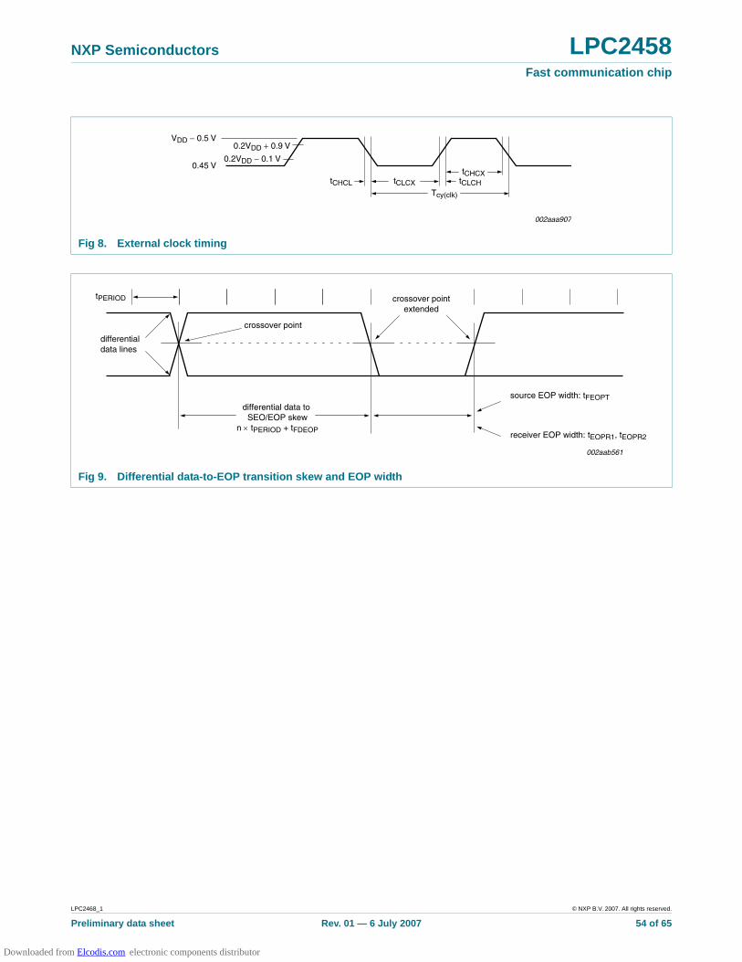
LPC2468_1 © NXP B.V. 2007. All rights reserved.
Prelim inary da ta sheet Rev. 01 — 6 July 2007 54 of 65
NXP Semiconductors LPC2458Fast communica tion ch ip
Fig 8. External clock timing
tCHCL tCLCX
tCHCX
Tcy(clk)
tCLCH
002aaa907
0.2VDD + 0.9 V
0.2VDD − 0.1 V
VDD − 0.5 V
0.45 V
Fig 9. Differ ential dat a-to-EOP trans ition skew and EOP wid th
002aab561
tPERIOD
differential
data lines
crossover point
source EOP width: tFEOPT
receiver EOP width: tEOPR1, tEOPR2
crossover point
extended
differential data to
SEO/EOP skew
n u tPERIOD + tFDEOP
Downloaded from Elcodis.com electronic components distributor
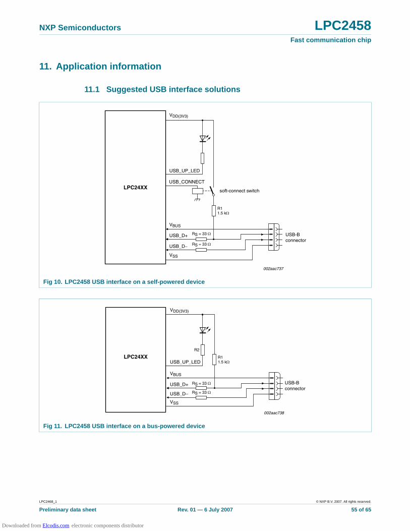
LPC2468_1 © NXP B.V. 2007. All rights reserved.
Prelim inary da ta sheet Rev. 01 — 6 July 2007 55 of 65
NXP Semiconductors LPC2458Fast communica tion ch ip
11. Application information
11.1 Sugg ested USB in terface solu tions
Fig 10. LPC2458 USB in terfa ce on a self-p owere d device
Fig 11. LPC2458 USB in terfa ce on a bus-powered device
LPC24XX
USB-B
connectorUSB_D+
USB_CONNECT
soft-connect switch
USB_D�
VBUS
VSS
VDD(3V3)
R11.5 k:
RS = 33 :
002aac737
RS = 33 :
USB_UP_LED
LPC24XX
VDD(3V3)
R11.5 k:
R2
USB_UP_LED
002aac738
USB-B
connectorUSB_D+
USB_D−
VBUS
VSS
RS = 33 :
RS = 33 :
Downloaded from Elcodis.com electronic components distributor

LPC2468_1 © NXP B.V. 2007. All rights reserved.
Prelim inary da ta sheet Rev. 01 — 6 July 2007 56 of 65
NXP Semiconductors LPC2458Fast communica tion ch ip
Fig 12. LPC2458 USB OTG port c onfiguration: USB port 1 OTG dual-role device, USB po rt 2 host
USB_UP_LED1
USB_D+1
USB_D�1
USB_PWRD2
USB_SDA1
USB_SCL1
RSTOUT
15 k: 15 k:
LPC24XX
USB-A
connector
Mini-AB
connector
33 :
33 :
33 :
33 :
VDD
VDD
VDD
USB_UP_LED2
VDD
USB_OVRCR2
LM3526-LENA
IN
5 V
OUTA
FLAGA
VDD
D+
D�
VBUS
USB_PPWR2
USB_D+2
USB_D�2
002aac708
R7
R4 R5 R6
R1 R2 R3 R4
R8
USB_INT1
RESET_N
ADR/PSW
SPEED
SUSPEND
OE_N/INT_N
SCL
SDA
INT_N
VBUS
ID
DP
DMISP1301
VSS
VSS
Downloaded from Elcodis.com electronic components distributor
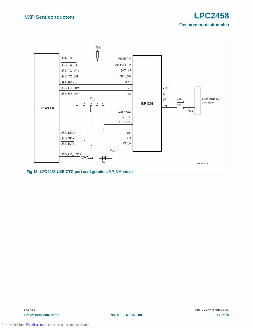
LPC2468_1 © NXP B.V. 2007. All rights reserved.
Prelim inary da ta sheet Rev. 01 — 6 July 2007 57 of 65
NXP Semiconductors LPC2458Fast communica tion ch ip
Fig 13. LPC2458 USB OTG port c onfiguration: VP_VM mod e
USB_TX_DP1
USB_TX_DM1
USB_RCV1
USB_RX_DP1
USB_RX_DM1
USB_SCL1
USB_SDA1
SPEED
ADR/PSW
SDA
SCL
RESET_N
INT_N
VP
VM
SUSPEND
OE_N/INT_N
SE0_VM
DAT_VP
RCV
VBUS
ID
DP
DMLPC24XX
ISP1301
USB MINI-AB
connector
33 :
33 :
002aac711
USB_TX_E1
RSTOUT
VDD
VDD
USB_INT1
USB_UP_LED1
VDD
VSS
Downloaded from Elcodis.com electronic components distributor

LPC2468_1 © NXP B.V. 2007. All rights reserved.
Prelim inary da ta sheet Rev. 01 — 6 July 2007 58 of 65
NXP Semiconductors LPC2458Fast communica tion ch ip
Fig 14. LPC2458 USB OTG port co nfigu ration : USB port 2 device, USB po rt 1 host
USB_UP_LED1
USB_D+1
USB_D�1
USB_PWRD1
15 k: 15 k:
LPC24XX
USB-A
connect
USB-B
connect
33 :
33 :
33 :
33 :
002aac710
VDD
USB_UP_LED2
USB_CONNECT2
VDD
VDD
USB_OVRCR1
USB_PPWR1
LM3526-L
ENA
IN
5 V
FLAGA
OUTA
VDD
D+
D�
D+
D�
VBUS
USB_D+2
USB_D�2
VBUS VBUS
VSS
VSS
Downloaded from Elcodis.com electronic components distributor

LPC2468_1 © NXP B.V. 2007. All rights reserved.
Prelim inary da ta sheet Rev. 01 — 6 July 2007 59 of 65
NXP Semiconductors LPC2458Fast communica tion ch ip
Fig 15. LPC2458 USB OTG port c onfiguration: USB port 1 host, USB port 2 host
USB_UP_LED1
USB_D+1
USB_D�1
USB_PWRD1
USB_PWRD2
15 k:
15 k: 15 k:
15 k:
LPC24XX
USB-A
connecto
USB-A
connecto
33 :
33 :
33 :
33 :
002aac709
VDD
USB_UP_LED2
VDD
USB_OVRCR1
USB_OVRCR2
USB_PPWR1
LM3526-L
ENA
ENB
IN
5 V
FLAGA
OUTA
OUTB
FLAGB
VDD
VDD
D+
D�
D+
D�
VBUS
VBUS
USB_PPWR2
USB_D+2
USB_D�2
VSS
VSS
Downloaded from Elcodis.com electronic components distributor

LPC2468_1 © NXP B.V. 2007. All rights reserved.
Prelim inary da ta sheet Rev. 01 — 6 July 2007 60 of 65
NXP Semiconductors LPC2458Fast communica tion ch ip
12. Package outline
Fig 16. Package outlin e SOT570-2 (TFBGA180)
0.8
A1 bA2UNIT D ye
REFERENCESOUTLINE
VERSION
EUROPEAN
PROJECTIONISSUE DATE
03-03-03
06-03-14
IEC JEDEC JEITA
mm 1.20.35
0.25
0.85
0.75
12.2
11.8
y1
12.2
11.8
0.5
0.40.12 0.1
e1
10.4
e2
10.4
DIMENSIONS (mm are the original dimensions)
SOT570-2
E
0.15
v
0.08
w
0 5 10 mm
scale
SOT570-2TFBGA180: thin fine-pitch ball grid array package; 180 balls; body 12 x 12 x 0.8 mm
A
max.
AA2
A1
detail X
e
e
X
D
E
A
B
C
D
E
F
H
G
J
K
L
M
N
P
2 4 6 981 3 5 7 10 13 141211
B A
e2
e1
ball A1
index area
ball A1
index area
1/2 e
1/2 e
yy1 Cb
C
AC
C
B∅ v M
∅ w M
Downloaded from Elcodis.com electronic components distributor
LPC2468_1 © NXP B.V. 2007. All rights reserved.
Prelim inary da ta sheet Rev. 01 — 6 July 2007 61 of 65
NXP Semiconductors LPC2458Fast communica tion ch ip
13. Abbreviations
Table 13. Acronym lis t
Acronym Descrip tion
ADC Analog-to-Digital Converter
AHB Advanced High-performance Bus
AMBA Advanced Microcontroller Bus Architecture
APB Advanced Peripheral Bus
ATX Analog Transceiver
BLS Byte Lane Select
BOD BrownOut Detection
CAN Controller Area Network
DAC Digital-to-Analog Converter
DCC Debug Communication Channel
DMA Direct Memory Access
DSP Digital Signal Processing
EOP End Of Packet
ETM Embedded Trace Macrocell
GPIO General Purpose Input/Output
JTAG Joint Test Action Group
MII Media Independent Interface
PHY Physical Layer
PLL Phase-Locked Loop
PWM Pulse Width Modulator
RMII Reduced Media Independent Interface
SD/MMC Secure Digital/MultiMediaCard
SE0 Single Ended Zero
SPI Serial Peripheral Interface
SSI Synchronous Serial Interface
SSP Synchronous Serial Port
TTL Transistor-Transistor Logic
UART Universal Asynchronous Receiver/Transmitter
USB Universal Serial Bus
Downloaded from Elcodis.com electronic components distributor

LPC2468_1 © NXP B.V. 2007. All rights reserved.
Prelim inary da ta sheet Rev. 01 — 6 July 2007 62 of 65
NXP Semiconductors LPC2458Fast communica tion ch ip
14. Revision history
Table 14. Revis ion hist ory
Document ID Release date Data sheet st atus Change notice Supersed es
LPC2458_1 <tbd> Preliminary data sheet - -
Downloaded from Elcodis.com electronic components distributor

LPC2468_1 © NXP B.V. 2007. All rights reserved.
Prelim inary da ta sheet Rev. 01 — 6 July 2007 63 of 65
NXP Semiconductors LPC2458Fast communica tion ch ip
15. Legal information
15.1 Data sheet st atus
[1] Please consult the most recently issued document before initiating or completing a design.
[2] The term ‘short data sheet’ is explained in section “Definitions”.
[3] The product status of device(s) described in this document may have changed since this document was published and may differ in case of multiple devices. The latest product status information is available on the Internet at URL http://www.nxp.com.
15.2 Definitions
Draft — The document is a draft version only. The content is still under internal review and subject to formal approval, which may result in modifications or additions. NXP Semiconductors does not give any representations or warranties as to the accuracy or completeness of information included herein and shall have no liability for the consequences of use of such information.
Short data sheet — A short data sheet is an extract from a full data sheet with the same product type number(s) and title. A short data sheet is intended for quick reference only and should not be relied upon to contain detailed and full information. For detailed and full information see the relevant full data sheet, which is available on request via the local NXP Semiconductors sales office. In case of any inconsistency or conflict with the short data sheet, the full data sheet shall prevail.
15.3 Disclaimers
General — Information in this document is believed to be accurate and reliable. However, NXP Semiconductors does not give any representations or warranties, expressed or implied, as to the accuracy or completeness of such information and shall have no liability for the consequences of use of such information.
Right to m ake changes — NXP Semiconductors reserves the right to make changes to information published in this document, including without limitation specifications and product descriptions, at any time and without notice. This document supersedes and replaces all information supplied prior to the publication hereof.
Suitabil ity for use — NXP Semiconductors products are not designed, authorized or warranted to be suitable for use in medical, military, aircraft, space or life support equipment, nor in applications where failure or malfunction of a NXP Semiconductors product can reasonably be expected to result in personal injury, death or severe property or environmental damage.
NXP Semiconductors accepts no liability for inclusion and/or use of NXP Semiconductors products in such equipment or applications and therefore such inclusion and/or use is at the customer’s own risk.
Applic ation s — Applications that are described herein for any of these products are for illustrative purposes only. NXP Semiconductors makes no representation or warranty that such applications will be suitable for the specified use without further testing or modification.
Limi ting v alues — Stress above one or more limiting values (as defined in the Absolute Maximum Ratings System of IEC 60134) may cause permanent damage to the device. Limiting values are stress ratings only and operation of the device at these or any other conditions above those given in the Characteristics sections of this document is not implied. Exposure to limiting values for extended periods may affect device reliability.
Terms and condi tions o f sale — NXP Semiconductors products are sold subject to the general terms and conditions of commercial sale, as published at http://www.nxp.com/profile/terms, including those pertaining to warranty, intellectual property rights infringement and limitation of liability, unless explicitly otherwise agreed to in writing by NXP Semiconductors. In case of any inconsistency or conflict between information in this document and such terms and conditions, the latter will prevail.
No offe r to sel l or l icense — Nothing in this document may be interpreted or construed as an offer to sell products that is open for acceptance or the grant, conveyance or implication of any license under any copyrights, patents or other industrial or intellectual property rights.
15.4 TrademarksNotice: All referenced brands, product names, service names and trademarks are the property of their respective owners.
I2C-bus — logo is a trademark of NXP B.V.
SoftConnect — is a trademark of NXP B.V.
GoodL ink — is a trademark of NXP B.V.
16. Contact information
For additional information, please visit: http://w ww.nxp. com
For sales office addresses, send an email to: salesaddre [email protected]
Document status[1][2] Prod uct s tatus[3] Definiti on
Objective [short] data sheet Development This document contains data from the objective specification for product development.
Preliminary [short] data sheet Qualification This document contains data from the preliminary specification.
Product [short] data sheet Production This document contains the product specification.
Downloaded from Elcodis.com electronic components distributor
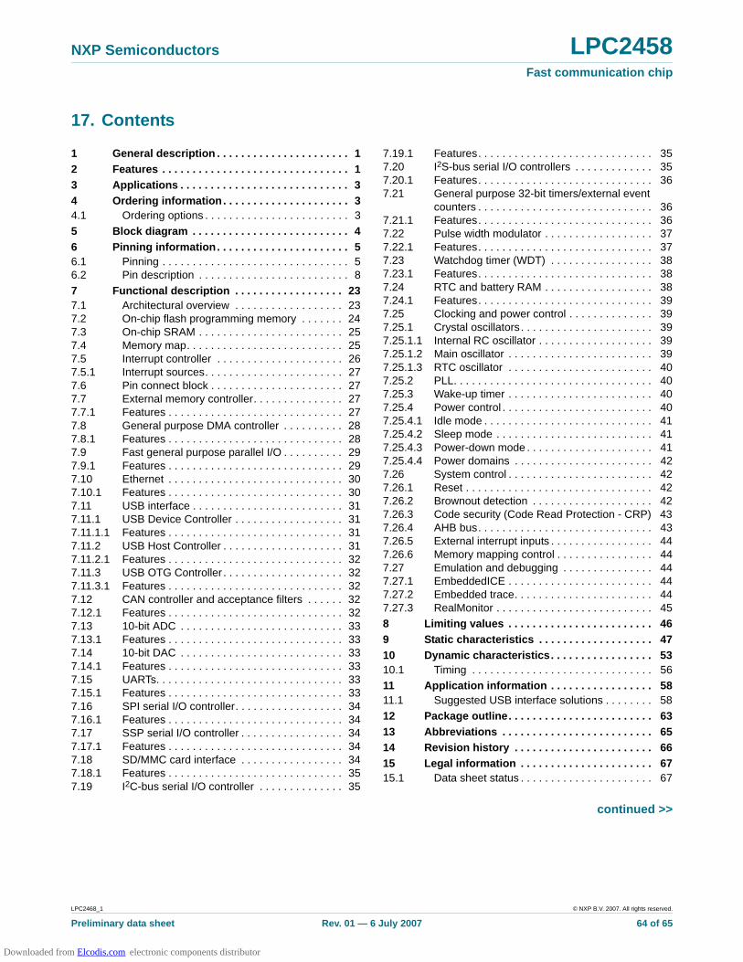
LPC2468_1 © NXP B.V. 2007. All rights reserved.
Prelim inary da ta sheet Rev. 01 — 6 July 2007 64 of 65
cont inued >>
NXP Semiconductors LPC2458Fast communica tion ch ip
17. Content s
1 General descrip tion . . . . . . . . . . . . . . . . . . . . . . 12 Features . . . . . . . . . . . . . . . . . . . . . . . . . . . . . . . 13 Applicati ons . . . . . . . . . . . . . . . . . . . . . . . . . . . . 34 Ordering in formatio n . . . . . . . . . . . . . . . . . . . . . 34.1 Ordering options . . . . . . . . . . . . . . . . . . . . . . . . 3
5 Block diag ram . . . . . . . . . . . . . . . . . . . . . . . . . . 46 Pinning informatio n . . . . . . . . . . . . . . . . . . . . . . 56.1 Pinning . . . . . . . . . . . . . . . . . . . . . . . . . . . . . . . 56.2 Pin description . . . . . . . . . . . . . . . . . . . . . . . . . 8
7 Functi onal descri ption . . . . . . . . . . . . . . . . . . 237.1 Architectural overview . . . . . . . . . . . . . . . . . . 237.2 On-chip flash programming memory . . . . . . . 247.3 On-chip SRAM . . . . . . . . . . . . . . . . . . . . . . . . 257.4 Memory map. . . . . . . . . . . . . . . . . . . . . . . . . . 257.5 Interrupt controller . . . . . . . . . . . . . . . . . . . . . 267.5.1 Interrupt sources. . . . . . . . . . . . . . . . . . . . . . . 277.6 Pin connect block . . . . . . . . . . . . . . . . . . . . . . 277.7 External memory controller. . . . . . . . . . . . . . . 277.7.1 Features . . . . . . . . . . . . . . . . . . . . . . . . . . . . . 277.8 General purpose DMA controller . . . . . . . . . . 287.8.1 Features . . . . . . . . . . . . . . . . . . . . . . . . . . . . . 287.9 Fast general purpose parallel I/O . . . . . . . . . . 297.9.1 Features . . . . . . . . . . . . . . . . . . . . . . . . . . . . . 297.10 Ethernet . . . . . . . . . . . . . . . . . . . . . . . . . . . . . 307.10.1 Features . . . . . . . . . . . . . . . . . . . . . . . . . . . . . 307.11 USB interface . . . . . . . . . . . . . . . . . . . . . . . . . 317.11.1 USB Device Controller . . . . . . . . . . . . . . . . . . 317.11.1.1 Features . . . . . . . . . . . . . . . . . . . . . . . . . . . . . 317.11.2 USB Host Controller . . . . . . . . . . . . . . . . . . . . 317.11.2.1 Features . . . . . . . . . . . . . . . . . . . . . . . . . . . . . 327.11.3 USB OTG Controller . . . . . . . . . . . . . . . . . . . . 327.11.3.1 Features . . . . . . . . . . . . . . . . . . . . . . . . . . . . . 327.12 CAN controller and acceptance filters . . . . . . 327.12.1 Features . . . . . . . . . . . . . . . . . . . . . . . . . . . . . 327.13 10-bit ADC . . . . . . . . . . . . . . . . . . . . . . . . . . . 337.13.1 Features . . . . . . . . . . . . . . . . . . . . . . . . . . . . . 337.14 10-bit DAC . . . . . . . . . . . . . . . . . . . . . . . . . . . 337.14.1 Features . . . . . . . . . . . . . . . . . . . . . . . . . . . . . 337.15 UARTs. . . . . . . . . . . . . . . . . . . . . . . . . . . . . . . 337.15.1 Features . . . . . . . . . . . . . . . . . . . . . . . . . . . . . 337.16 SPI serial I/O controller. . . . . . . . . . . . . . . . . . 347.16.1 Features . . . . . . . . . . . . . . . . . . . . . . . . . . . . . 347.17 SSP serial I/O controller . . . . . . . . . . . . . . . . . 347.17.1 Features . . . . . . . . . . . . . . . . . . . . . . . . . . . . . 347.18 SD/MMC card interface . . . . . . . . . . . . . . . . . 347.18.1 Features . . . . . . . . . . . . . . . . . . . . . . . . . . . . . 357.19 I2C-bus serial I/O controller . . . . . . . . . . . . . . 35
7.19.1 Features. . . . . . . . . . . . . . . . . . . . . . . . . . . . . 357.20 I2S-bus serial I/O controllers . . . . . . . . . . . . . 357.20.1 Features. . . . . . . . . . . . . . . . . . . . . . . . . . . . . 367.21 General purpose 32-bit timers/external event
counters . . . . . . . . . . . . . . . . . . . . . . . . . . . . . 367.21.1 Features. . . . . . . . . . . . . . . . . . . . . . . . . . . . . 367.22 Pulse width modulator . . . . . . . . . . . . . . . . . . 377.22.1 Features. . . . . . . . . . . . . . . . . . . . . . . . . . . . . 377.23 Watchdog timer (WDT) . . . . . . . . . . . . . . . . . 387.23.1 Features. . . . . . . . . . . . . . . . . . . . . . . . . . . . . 387.24 RTC and battery RAM . . . . . . . . . . . . . . . . . . 387.24.1 Features. . . . . . . . . . . . . . . . . . . . . . . . . . . . . 397.25 Clocking and power control . . . . . . . . . . . . . . 397.25.1 Crystal oscillators. . . . . . . . . . . . . . . . . . . . . . 397.25.1.1 Internal RC oscillator . . . . . . . . . . . . . . . . . . . 397.25.1.2 Main oscillator . . . . . . . . . . . . . . . . . . . . . . . . 397.25.1.3 RTC oscillator . . . . . . . . . . . . . . . . . . . . . . . . 407.25.2 PLL. . . . . . . . . . . . . . . . . . . . . . . . . . . . . . . . . 407.25.3 Wake-up timer . . . . . . . . . . . . . . . . . . . . . . . . 407.25.4 Power control . . . . . . . . . . . . . . . . . . . . . . . . . 407.25.4.1 Idle mode . . . . . . . . . . . . . . . . . . . . . . . . . . . . 417.25.4.2 Sleep mode . . . . . . . . . . . . . . . . . . . . . . . . . . 417.25.4.3 Power-down mode . . . . . . . . . . . . . . . . . . . . . 417.25.4.4 Power domains . . . . . . . . . . . . . . . . . . . . . . . 427.26 System control . . . . . . . . . . . . . . . . . . . . . . . . 427.26.1 Reset . . . . . . . . . . . . . . . . . . . . . . . . . . . . . . . 427.26.2 Brownout detection . . . . . . . . . . . . . . . . . . . . 427.26.3 Code security (Code Read Protection - CRP) 437.26.4 AHB bus. . . . . . . . . . . . . . . . . . . . . . . . . . . . . 437.26.5 External interrupt inputs . . . . . . . . . . . . . . . . . 447.26.6 Memory mapping control . . . . . . . . . . . . . . . . 447.27 Emulation and debugging . . . . . . . . . . . . . . . 447.27.1 EmbeddedICE . . . . . . . . . . . . . . . . . . . . . . . . 447.27.2 Embedded trace. . . . . . . . . . . . . . . . . . . . . . . 447.27.3 RealMonitor . . . . . . . . . . . . . . . . . . . . . . . . . . 458 Limitin g values . . . . . . . . . . . . . . . . . . . . . . . . 469 Static characteristics . . . . . . . . . . . . . . . . . . . 4710 Dynamic ch aracteristics . . . . . . . . . . . . . . . . . 5310.1 Timing . . . . . . . . . . . . . . . . . . . . . . . . . . . . . . 5611 App lication in format ion . . . . . . . . . . . . . . . . . 5811.1 Suggested USB interface solutions . . . . . . . . 58
12 Package o utlin e. . . . . . . . . . . . . . . . . . . . . . . . 6313 Abb reviatio ns . . . . . . . . . . . . . . . . . . . . . . . . . 6514 Revision history . . . . . . . . . . . . . . . . . . . . . . . 6615 Legal in formatio n . . . . . . . . . . . . . . . . . . . . . . 6715.1 Data sheet status . . . . . . . . . . . . . . . . . . . . . . 67
Downloaded from Elcodis.com electronic components distributor

NXP Semiconductors LPC2458Fast communica tion ch ip
© NXP B.V. 2007. All rights reserved.For more information, please visit: http://www.nxp.comFor sales office addresses, please send an email to: [email protected]
Date of rele ase: 6 July 2007
Document identifier: LPC2468_1
Please be aware that important notices concerning this document and the product(s)described herein, have been included in section ‘Legal information’.
15.2 Definitions. . . . . . . . . . . . . . . . . . . . . . . . . . . . 6715.3 Disclaimers . . . . . . . . . . . . . . . . . . . . . . . . . . . 6715.4 Trademarks. . . . . . . . . . . . . . . . . . . . . . . . . . . 67
16 Contact i nformatio n . . . . . . . . . . . . . . . . . . . . . 6717 Content s . . . . . . . . . . . . . . . . . . . . . . . . . . . . . . 68
Downloaded from Elcodis.com electronic components distributor


![ELCODIS.COM - ELECTRONIC COMPONENTS DISTRIBUTORdatasheet.elcodis.com/pdf2/73/7/730774/m63016fp.pdf · MITSUBISHI SEMICONDUCTORS M63016FP Spindle Motor AND 4CH ACTUATOR Drive IC [FEATURES]](https://static.fdocuments.net/doc/165x107/60d8ba5e32d4de45ed059731/-electronic-components-distributordatasheetelcodiscompdf2737730774m63016fppdf.jpg)