± 4g / 8g / 16g Tri axis Digital KXCJK Accelerometer ... · ± 4g / 8g / 16g Tri-axis Digital...
31
± 4g / 8g / 16g Tri-axis Digital Accelerometer Specifications PART NUMBER: KXCJK-1038 Rev. 2 Sep-2014 36 Thornwood Dr. – Ithaca, NY 14850 © 2014 Kionix – All Rights Reserved tel: 607-257-1080 – fax:607-257-1146 665-4730:6142M-1408071650 www.kionix.com - [email protected] Page 1 of 31 Product Description The KXCJK-1038 is a tri-axis +/-4g, +/-8g or +/-16g silicon micromachined accelerometer. The sense element is fabricated using Kionix’s proprietary plasma micromachining process technology. Acceleration sensing is based on the principle of a differential capacitance arising from acceleration-induced motion of the sense element, which further utilizes common mode cancellation to decrease errors from process variation, temperature, and environmental stress. The sense element is hermetically sealed at the wafer level by bonding a second silicon lid wafer to the device using a glass frit. A separate ASIC device packaged with the sense element provides signal conditioning and digital communications. The accelerometer is delivered in a 3 x 3 x 0.9 mm LGA plastic package operating from a 1.8 – 3.6V DC supply. Voltage regulators are used to maintain constant internal operating voltages over the range of input supply voltages. This results in stable operating characteristics over the range of input supply voltages and virtually undetectable ratiometric error. The I 2 C digital protocol is used to communicate with the chip to configure the part and monitor outputs.
Transcript of ± 4g / 8g / 16g Tri axis Digital KXCJK Accelerometer ... · ± 4g / 8g / 16g Tri-axis Digital...
± 4g / 8g / 16g Tri-axis Digital Accelerometer Specifications
PART NUMBER:
KXCJK-1038 Rev. 2
Sep-2014
36 Thornwood Dr. – Ithaca, NY 14850 © 2014 Kionix – All Rights Reserved tel: 607-257-1080 – fax:607-257-1146 665-4730:6142M-1408071650
www.kionix.com - [email protected] Page 1 of 31
Product Description
The KXCJK-1038 is a tri-axis +/-4g, +/-8g or +/-16g silicon
micromachined accelerometer. The sense element is
fabricated using Kionix’s proprietary plasma micromachining
process technology. Acceleration sensing is based on the
principle of a differential capacitance arising from
acceleration-induced motion of the sense element, which
further utilizes common mode cancellation to decrease errors
from process variation, temperature, and environmental
stress. The sense element is hermetically sealed at the wafer
level by bonding a second silicon lid wafer to the device using
a glass frit. A separate ASIC device packaged with the sense
element provides signal conditioning and digital
communications. The accelerometer is delivered in a 3 x 3 x
0.9 mm LGA plastic package operating from a 1.8 – 3.6V DC
supply. Voltage regulators are used to maintain constant
internal operating voltages over the range of input supply
voltages. This results in stable operating characteristics over
the range of input supply voltages and virtually undetectable ratiometric error. The I2C digital
protocol is used to communicate with the chip to configure the part and monitor outputs.
± 4g / 8g / 16g Tri-axis Digital Accelerometer Specifications
PART NUMBER:
KXCJK-1038 Rev. 2
Sep-2014
36 Thornwood Dr. – Ithaca, NY 14850 © 2014 Kionix – All Rights Reserved tel: 607-257-1080 – fax:607-257-1146 665-4730:6142M-1408071650
www.kionix.com - [email protected] Page 2 of 31
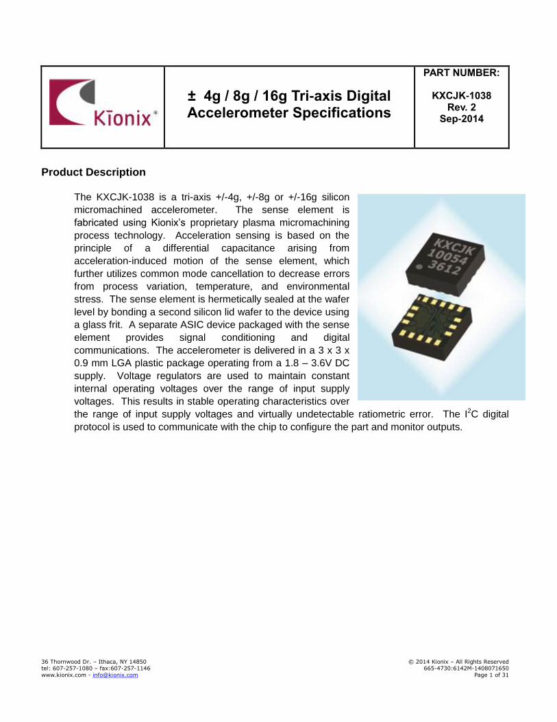
Functional Diagram
X Sensor
Vdd
IO Vdd
GND
Y Sensor
Z Sensor
4 7
I 2 C Digital Engine
Charge Amp
14
1
5
A / D
6 11
Digital Filter
ADDR SCL SDA INT
± 4g / 8g / 16g Tri-axis Digital Accelerometer Specifications
PART NUMBER:
KXCJK-1038 Rev. 2
Sep-2014
36 Thornwood Dr. – Ithaca, NY 14850 © 2014 Kionix – All Rights Reserved tel: 607-257-1080 – fax:607-257-1146 665-4730:6142M-1408071650
www.kionix.com - [email protected] Page 3 of 31
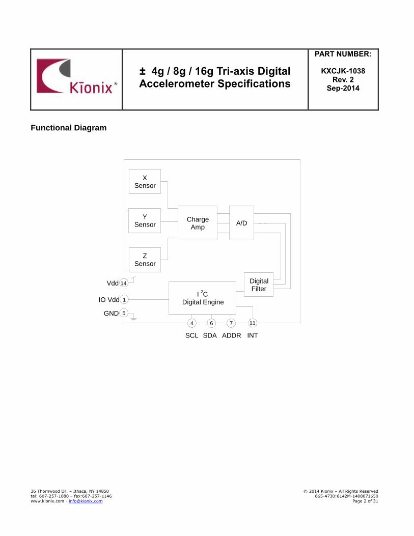
Product Specifications
Table 1. Mechanical (specifications are for operation at 2.6V and T = 25C unless stated otherwise)
Parameters Units Min Typical Max
Operating Temperature Range ºC -40 - 85
Zero-g Off
set mg - ±25 ±125
Zero-g Offset Variation from RT over Temp. mg/ºC 0.2
Sensitivity (14-bit)1,2
GSEL1=1, GSEL0=1 (± 16g) counts/g 461 512 563
Sensitivity (12-bit)1
GSEL1=0, GSEL0=0 (± 4g)
counts/g
461 512 563
GSEL1=0, GSEL0=1 (± 8g) 230 256 282
GSEL1=1, GSEL0=0 (± 16g) 115 128 141
Sensitivity (8-bit)1
GSEL1=0, GSEL0=0 (± 4g)
counts/g
27 32 36
GSEL1=0, GSEL0=1 (± 8g) 14 16 18
GSEL1=1, GSEL0=0 (± 16g) 17 8 9
Sensitivity Variation from RT over Temp. %/ºC 0.03
Self Test Output g
1 (x) 0.8 (y) 0.6 (z)
Mechanical Resonance (-3dB)3 Hz
3500 (xy) 1800 (z)
Non-Linearity % of FS 0.6
Cross Axis Sensitivity % 2
Notes:
1. Resolution and acceleration ranges are user selectable via I2C.
2. 14-bit Resolution is only available for registers 0x06h – 0x0Bh in the 16g Full Power mode 3. Resonance as defined by the dampened mechanical sensor.
± 4g / 8g / 16g Tri-axis Digital Accelerometer Specifications
PART NUMBER:
KXCJK-1038 Rev. 2
Sep-2014
36 Thornwood Dr. – Ithaca, NY 14850 © 2014 Kionix – All Rights Reserved tel: 607-257-1080 – fax:607-257-1146 665-4730:6142M-1408071650
www.kionix.com - [email protected] Page 4 of 31
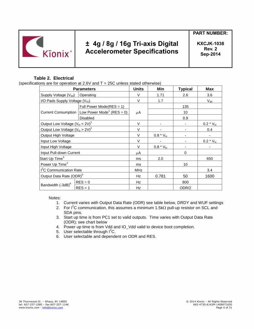
Table 2. Electrical (specifications are for operation at 2.6V and T = 25C unless stated otherwise)
Parameters Units Min Typical Max
Supply Voltage (Vdd) Operating V 1.71 2.6 3.6
I/O Pads Supply Voltage (VIO) V 1.7 Vdd
Current Consumption
Full Power Mode(RES = 1)
A
135
Low Power Mode1 (RES = 0) 10
Disabled 0.9
Output Low Voltage (Vio < 2V)2 V - - 0.2 * Vio
Output Low Voltage (Vio > 2V)2 V - - 0.4
Output High Voltage V 0.8 * Vio - -
Input Low Voltage V - - 0.2 * Vio
Input High Voltage V 0.8 * Vio - -
Input Pull-down Current A 0
Start Up Time3 ms 2.0 650
Power Up Time4 ms 10
I2C Communication Rate MHz 3.4
Output Data Rate (ODR)5 Hz 0.781 50 1600
Bandwidth (-3dB)6
RES = 0 Hz 800
RES = 1 Hz ODR/2
Notes:
1. Current varies with Output Data Rate (ODR) see table below, DRDY and WUF settings
2. For I2C communication, this assumes a minimum 1.5k pull-up resistor on SCL and
SDA pins. 3. Start up time is from PC1 set to valid outputs. Time varies with Output Data Rate
(ODR); see chart below 4. Power up time is from Vdd and IO_Vdd valid to device boot completion. 5. User selectable through I
2C.
6. User selectable and dependent on ODR and RES.
± 4g / 8g / 16g Tri-axis Digital Accelerometer Specifications
PART NUMBER:
KXCJK-1038 Rev. 2
Sep-2014
36 Thornwood Dr. – Ithaca, NY 14850 © 2014 Kionix – All Rights Reserved tel: 607-257-1080 – fax:607-257-1146 665-4730:6142M-1408071650
www.kionix.com - [email protected] Page 5 of 31
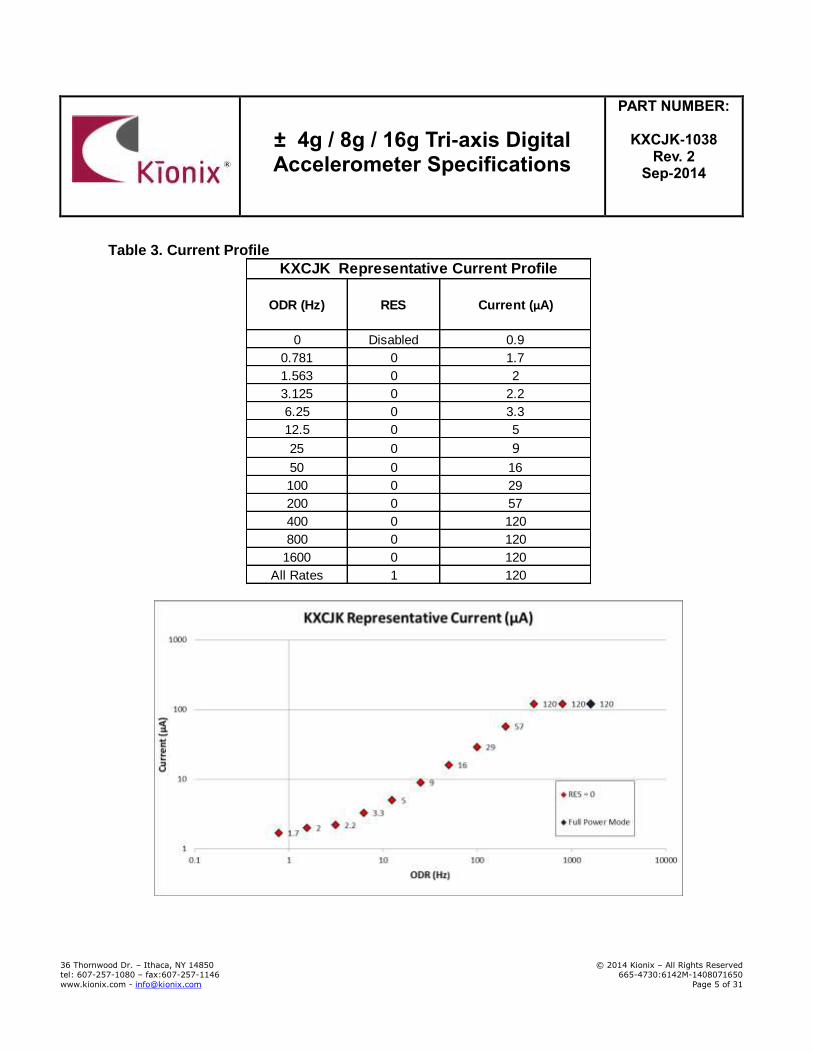
Table 3. Current Profile
ODR (Hz) RES Current (μA)
0 Disabled 0.9
0.781 0 1.7
1.563 0 2
3.125 0 2.2
6.25 0 3.3
12.5 0 5
25 0 9
50 0 16
100 0 29
200 0 57
400 0 120
800 0 120
1600 0 120
All Rates 1 120
KXCJK Representative Current Profile
± 4g / 8g / 16g Tri-axis Digital Accelerometer Specifications
PART NUMBER:
KXCJK-1038 Rev. 2
Sep-2014
36 Thornwood Dr. – Ithaca, NY 14850 © 2014 Kionix – All Rights Reserved tel: 607-257-1080 – fax:607-257-1146 665-4730:6142M-1408071650
www.kionix.com - [email protected] Page 6 of 31
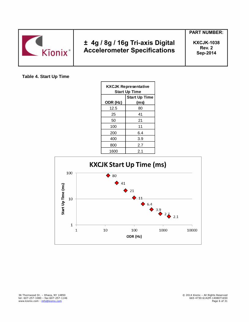
Table 4. Start Up Time
ODR (Hz)
Start Up Time
(ms)
12.5 80
25 41
50 21
100 11
200 6.4
400 3.9
800 2.7
1600 2.1
KXCJK Representative
Start Up Time

± 4g / 8g / 16g Tri-axis Digital Accelerometer Specifications
PART NUMBER:
KXCJK-1038 Rev. 2
Sep-2014
36 Thornwood Dr. – Ithaca, NY 14850 © 2014 Kionix – All Rights Reserved tel: 607-257-1080 – fax:607-257-1146 665-4730:6142M-1408071650
www.kionix.com - [email protected] Page 7 of 31
HF
Table 5. Environmental
Parameters Units Min Typical Max
Supply Voltage (Vdd) Absolute Limits V -0.5 - 3.63
Operating Temperature Range ºC -40 - 85
Storage Temperature Range ºC -55 - 150
Mech. Shock (powered and unpowered) g - - 5000 for 0.5ms
10000 for 0.2ms
ESD HBM V - - 2000
Caution: ESD Sensitive and Mechanical Shock Sensitive Component, improper handling can cause permanent damage to the device.
This product conforms to Directive 2002/95/EC of the European Parliament and of the Council of the European Union (RoHS). Specifically, this product does not contain lead, mercury, cadmium, hexavalent chromium, polybrominated biphenyls (PBB), or polybrominated diphenyl ethers (PBDE) above the maximum concentration values (MCV) by weight in any of its homogenous materials. Homogenous materials are "of uniform
composition throughout."
This product is halogen-free per IEC 61249-2-21. Specifically, the materials used in this product contain a maximum total halogen content of 1500 ppm with less than 900-ppm bromine and less than 900-ppm chlorine.
Soldering
Soldering recommendations are available upon request or from www.kionix.com. Floor Life Factory floor life exposure of the KXCJK reels removed from the moisture barrier bag should not exceed a maximum of 168 hours at 30C/60%RH. If this floor life is exceeded, the parts should be dried per the IPC/JEDEC J-STD-033A standard.
± 4g / 8g / 16g Tri-axis Digital Accelerometer Specifications
PART NUMBER:
KXCJK-1038 Rev. 2
Sep-2014
36 Thornwood Dr. – Ithaca, NY 14850 © 2014 Kionix – All Rights Reserved tel: 607-257-1080 – fax:607-257-1146 665-4730:6142M-1408071650
www.kionix.com - [email protected] Page 8 of 31
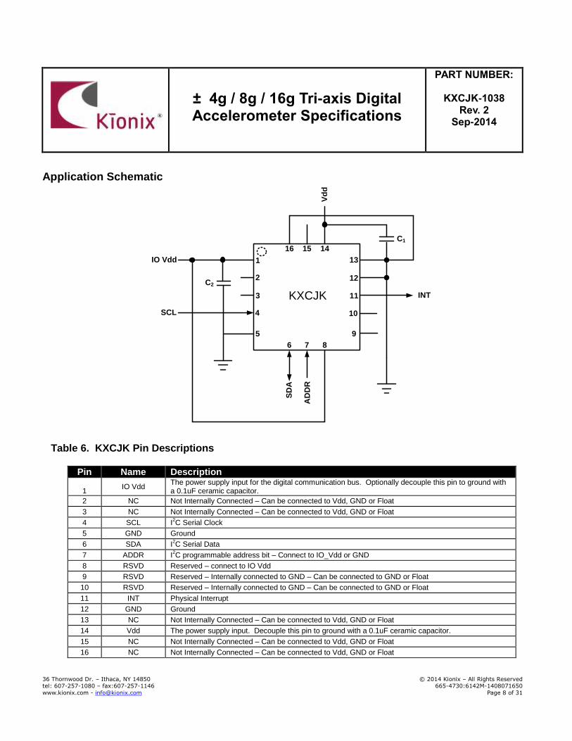
Application Schematic
1
2
3
5
7
9
11
12
13
Vd
d
C1
SD
AKXCJK INT
IO Vdd
C2
4SCL
86
15 1416
10A
DD
R
Table 6. KXCJK Pin Descriptions
Pin Name Description
1 IO Vdd
The power supply input for the digital communication bus. Optionally decouple this pin to ground with a 0.1uF ceramic capacitor.
2 NC Not Internally Connected – Can be connected to Vdd, GND or Float
3 NC Not Internally Connected – Can be connected to Vdd, GND or Float
4 SCL I2C Serial Clock
5 GND Ground
6 SDA I2C Serial Data
7 ADDR I2C programmable address bit – Connect to IO_Vdd or GND
8 RSVD Reserved – connect to IO Vdd
9 RSVD Reserved – Internally connected to GND – Can be connected to GND or Float
10 RSVD Reserved – Internally connected to GND – Can be connected to GND or Float
11 INT Physical Interrupt
12 GND Ground
13 NC Not Internally Connected – Can be connected to Vdd, GND or Float
14 Vdd The power supply input. Decouple this pin to ground with a 0.1uF ceramic capacitor.
15 NC Not Internally Connected – Can be connected to Vdd, GND or Float
16 NC Not Internally Connected – Can be connected to Vdd, GND or Float
± 4g / 8g / 16g Tri-axis Digital Accelerometer Specifications
PART NUMBER:
KXCJK-1038 Rev. 2
Sep-2014
36 Thornwood Dr. – Ithaca, NY 14850 © 2014 Kionix – All Rights Reserved tel: 607-257-1080 – fax:607-257-1146 665-4730:6142M-1408071650
www.kionix.com - [email protected] Page 9 of 31
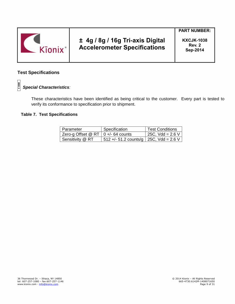
Test Specifications
! Special Characteristics:
These characteristics have been identified as being critical to the customer. Every part is tested to
verify its conformance to specification prior to shipment.
Table 7. Test Specifications
Parameter Specification Test Conditions
Zero-g Offset @ RT 0 +/- 64 counts 25C, Vdd = 2.6 V
Sensitivity @ RT 512 +/- 51.2 counts/g 25C, Vdd = 2.6 V
± 4g / 8g / 16g Tri-axis Digital Accelerometer Specifications
PART NUMBER:
KXCJK-1038 Rev. 2
Sep-2014
36 Thornwood Dr. – Ithaca, NY 14850 © 2014 Kionix – All Rights Reserved tel: 607-257-1080 – fax:607-257-1146 665-4730:6142M-1408071650
www.kionix.com - [email protected] Page 10 of 31
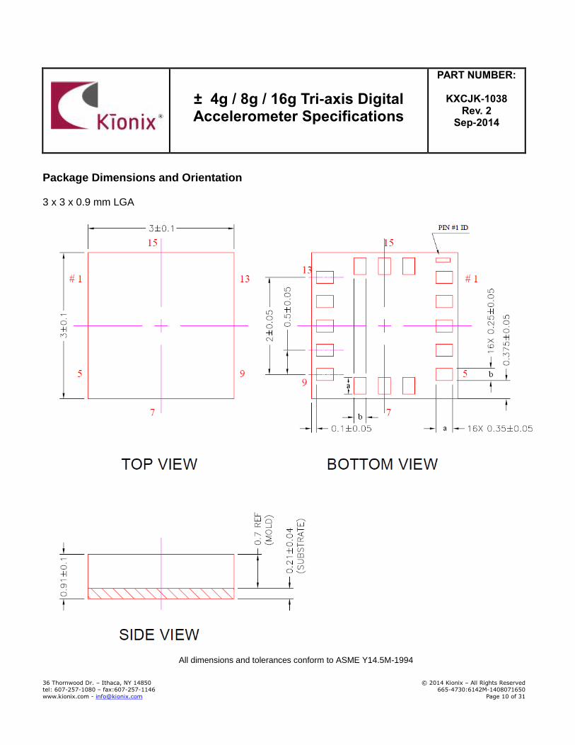
Package Dimensions and Orientation 3 x 3 x 0.9 mm LGA
All dimensions and tolerances conform to ASME Y14.5M-1994
± 4g / 8g / 16g Tri-axis Digital Accelerometer Specifications
PART NUMBER:
KXCJK-1038 Rev. 2
Sep-2014
36 Thornwood Dr. – Ithaca, NY 14850 © 2014 Kionix – All Rights Reserved tel: 607-257-1080 – fax:607-257-1146 665-4730:6142M-1408071650
www.kionix.com - [email protected] Page 11 of 31
Orientation
When device is accelerated in +X, +Y or +Z direction, the corresponding output will increase.
Static X/Y/Z Output Response versus Orientation to Earth’s surface (1g): GSEL1=0, GSEL0=0 (± 4g)
Position 1 2 3 4 5 6
Diagram
Top Bottom
Bottom Top
Resolution (bits) 12 8 12 8 12 8 12 8 12 8 12 8
X (counts) 0
0 -512
-32
0 0
512
32
0
0
0
0 Y (counts) -512
-32
0
0
512
32
0
0
0
0
0
0 Z (counts) 0 0 0 0 0
0
0 0 0 512 32 -512 -32
X-Polarity 0 - 0 + 0 0
Y-Polarity - 0 + 0 0 0
Z-Polarity 0 0 0 0 + -
(1g)
Earth’s Surface
Pin 1
+X
+Y
+Z
± 4g / 8g / 16g Tri-axis Digital Accelerometer Specifications
PART NUMBER:
KXCJK-1038 Rev. 2
Sep-2014
36 Thornwood Dr. – Ithaca, NY 14850 © 2014 Kionix – All Rights Reserved tel: 607-257-1080 – fax:607-257-1146 665-4730:6142M-1408071650
www.kionix.com - [email protected] Page 12 of 31
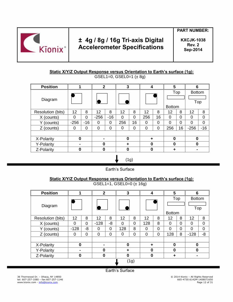
Static X/Y/Z Output Response versus Orientation to Earth’s surface (1g): GSEL1=0, GSEL0=1 (± 8g)
Position 1 2 3 4 5 6
Diagram
Top Bottom
Bottom Top
Resolution (bits) 12 8 12 8 12 8 12 8 12 8 12 8
X (counts) 0
0 -256
-16
0 0
256
16
0
0
0
0 Y (counts) -256
-16
0
0
256
16
0
0
0
0
0
0 Z (counts) 0 0 0 0 0
0
0 0 0 256 16 -256 -16
X-Polarity 0 - 0 + 0 0
Y-Polarity - 0 + 0 0 0
Z-Polarity 0 0 0 0 + -
(1g)
Earth’s Surface
Static X/Y/Z Output Response versus Orientation to Earth’s surface (1g):
GSEL1=1, GSEL0=0 (± 16g)
Position 1 2 3 4 5 6
Diagram
Top Bottom
Bottom Top
Resolution (bits) 12 8 12 8 12 8 12 8 12 8 12 8
X (counts) 0
0 -128
-8
0 0
128
8
0
0
0
0 Y (counts) -128
-8
0
0
128
8
0
0
0
0
0
0 Z (counts) 0 0 0 0 0
0
0 0 0 128 8 -128 -8
X-Polarity 0 - 0 + 0 0
Y-Polarity - 0 + 0 0 0
Z-Polarity 0 0 0 0 + -
(1g)
Earth’s Surface
± 4g / 8g / 16g Tri-axis Digital Accelerometer Specifications
PART NUMBER:
KXCJK-1038 Rev. 2
Sep-2014
36 Thornwood Dr. – Ithaca, NY 14850 © 2014 Kionix – All Rights Reserved tel: 607-257-1080 – fax:607-257-1146 665-4730:6142M-1408071650
www.kionix.com - [email protected] Page 13 of 31
KXCJK Digital Interface The Kionix KXCJK digital accelerometer has the ability to communicate on the I2C digital serial interface bus. This allows for easy system integration by eliminating analog-to-digital converter requirements and by providing direct communication with system micro-controllers. The serial interface terms and descriptions as indicated in Table 8 below will be observed throughout this document.
Term Description
Transmitter The device that transmits data to the bus.
Receiver The device that receives data from the bus.
Master The device that initiates a transfer, generates clock signals, and terminates a transfer.
Slave The device addressed by the Master.
Table 8. Serial Interface Terminologies
I2C Serial Interface As previously mentioned, the KXCJK has the ability to communicate on an I2C bus. I2C is primarily used for synchronous serial communication between a Master device and one or more Slave devices. The Master, typically a micro controller, provides the serial clock signal and addresses Slave devices on the bus. The KXCJK always operates as a Slave device during standard Master-Slave I2C operation. I2C is a two-wire serial interface that contains a Serial Clock (SCL) line and a Serial Data (SDA) line. SCL is a serial clock that is provided by the Master, but can be held low by any Slave device, putting the Master into a wait condition. SDA is a bi-directional line used to transmit and receive data to and from the interface. Data is transmitted MSB (Most Significant Bit) first in 8-bit per byte format, and the number of bytes transmitted per transfer is unlimited. The I2C bus is considered free when both lines are high. The I2C interface is compliant with high-speed mode, fast mode and standard mode I2C standards.
± 4g / 8g / 16g Tri-axis Digital Accelerometer Specifications
PART NUMBER:
KXCJK-1038 Rev. 2
Sep-2014
36 Thornwood Dr. – Ithaca, NY 14850 © 2014 Kionix – All Rights Reserved tel: 607-257-1080 – fax:607-257-1146 665-4730:6142M-1408071650
www.kionix.com - [email protected] Page 14 of 31
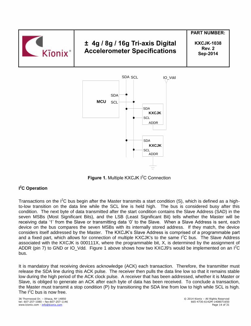
Figure 1. Multiple KXCJK I2C Connection
I2C Operation
Transactions on the I2C bus begin after the Master transmits a start condition (S), which is defined as a high-to-low transition on the data line while the SCL line is held high. The bus is considered busy after this condition. The next byte of data transmitted after the start condition contains the Slave Address (SAD) in the seven MSBs (Most Significant Bits), and the LSB (Least Significant Bit) tells whether the Master will be receiving data ‘1’ from the Slave or transmitting data ‘0’ to the Slave. When a Slave Address is sent, each device on the bus compares the seven MSBs with its internally stored address. If they match, the device considers itself addressed by the Master. The KXCJK’s Slave Address is comprised of a programmable part and a fixed part, which allows for connection of multiple KXCJK's to the same I2C bus. The Slave Address associated with the KXCJK is 000111X, where the programmable bit, X, is determined by the assignment of ADDR (pin 7) to GND or IO_Vdd. Figure 1 above shows how two KXCJ9's would be implemented on an I2C bus.
It is mandatory that receiving devices acknowledge (ACK) each transaction. Therefore, the transmitter must release the SDA line during this ACK pulse. The receiver then pulls the data line low so that it remains stable low during the high period of the ACK clock pulse. A receiver that has been addressed, whether it is Master or Slave, is obliged to generate an ACK after each byte of data has been received. To conclude a transaction, the Master must transmit a stop condition (P) by transitioning the SDA line from low to high while SCL is high. The I2C bus is now free.
MCU
KXCJK
SDA
SCL
IO_Vdd
ADDR
SCL
SCL
SDA
SDA SCL
SDA
ADDR
KXCJK

± 4g / 8g / 16g Tri-axis Digital Accelerometer Specifications
PART NUMBER:
KXCJK-1038 Rev. 2
Sep-2014
36 Thornwood Dr. – Ithaca, NY 14850 © 2014 Kionix – All Rights Reserved tel: 607-257-1080 – fax:607-257-1146 665-4730:6142M-1408071650
www.kionix.com - [email protected] Page 15 of 31
Writing to a KXCJK 8-bit Register Upon power up, the Master must write to the KXCJK’s control registers to set its operational mode. Therefore, when writing to a control register on the I2C bus, as shown Sequence 1 on the following page, the following protocol must be observed: After a start condition, SAD+W transmission, and the KXCJK ACK has been returned, an 8-bit Register Address (RA) command is transmitted by the Master. This command is telling the KXCJK to which 8-bit register the Master will be writing the data. Since this is I2C mode, the MSB of the RA command should always be zero (0). The KXCJK acknowledges the RA and the Master transmits the data to be stored in the 8-bit register. The KXCJK acknowledges that it has received the data and the Master transmits a stop condition (P) to end the data transfer. The data sent to the KXCJK is now stored in the appropriate register. The KXCJK automatically increments the received RA commands and, therefore, multiple bytes of data can be written to sequential registers after each Slave ACK as shown in Sequence 2 on the following page.
Reading from a KXCJK 8-bit Register When reading data from a KXCJK 8-bit register on the I2C bus, as shown in Sequence 3 on the next page, the following protocol must be observed: The Master first transmits a start condition (S) and the appropriate Slave Address (SAD) with the LSB set at ‘0’ to write. The KXCJK acknowledges and the Master transmits the 8-bit RA of the register it wants to read. The KXCJK again acknowledges, and the Master transmits a repeated start condition (Sr). After the repeated start condition, the Master addresses the KXCJK with a ‘1’ in the LSB (SAD+R) to read from the previously selected register. The Slave then acknowledges and transmits the data from the requested register. The Master does not acknowledge (NACK) it received the transmitted data, but transmits a stop condition to end the data transfer. Note that the KXCJK automatically increments through its sequential registers, allowing data to be read from multiple registers following a single SAD+R command as shown below in Sequence 4 on the following page. The 8-bit register data is transmitted using a left-most format, first bit shifted/clocked out being the MSB bit. If a receiver cannot transmit or receive another complete byte of data until it has performed some other function, it can hold SCL low to force the transmitter into a wait state. Data transfer only continues when the receiver is ready for another byte and releases SCL.
± 4g / 8g / 16g Tri-axis Digital Accelerometer Specifications
PART NUMBER:
KXCJK-1038 Rev. 2
Sep-2014
36 Thornwood Dr. – Ithaca, NY 14850 © 2014 Kionix – All Rights Reserved tel: 607-257-1080 – fax:607-257-1146 665-4730:6142M-1408071650
www.kionix.com - [email protected] Page 16 of 31
Data Transfer Sequences The following information clearly illustrates the variety of data transfers that can occur on the I2C bus and how the Master and Slave interact during these transfers. Table 9 defines the I2C terms used during the data transfers.
Term Definition
S Start Condition
Sr Repeated Start Condition
SAD Slave Address
W Write Bit
R Read Bit
ACK Acknowledge
NACK Not Acknowledge
RA Register Address
Data Transmitted/Received Data
P Stop Condition
Table 9. I2C Terms
Sequence 1. The Master is writing one byte to the Slave.
Master S SAD + W RA DATA P
Slave ACK ACK ACK
Sequence 2. The Master is writing multiple bytes to the Slave.
Master S SAD + W RA DATA DATA P
Slave ACK ACK ACK ACK
Sequence 3. The Master is receiving one byte of data from the Slave.
Master S SAD + W RA Sr SAD + R NACK P
Slave ACK ACK ACK DATA
Sequence 4. The Master is receiving multiple bytes of data from the Slave.
Master S SAD + W RA Sr SAD + R ACK NACK P
Slave ACK ACK ACK DATA DATA
± 4g / 8g / 16g Tri-axis Digital Accelerometer Specifications
PART NUMBER:
KXCJK-1038 Rev. 2
Sep-2014
36 Thornwood Dr. – Ithaca, NY 14850 © 2014 Kionix – All Rights Reserved tel: 607-257-1080 – fax:607-257-1146 665-4730:6142M-1408071650
www.kionix.com - [email protected] Page 17 of 31
KXCJK Embedded Registers
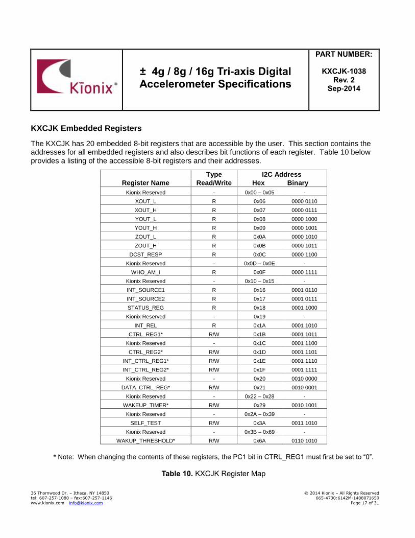
The KXCJK has 20 embedded 8-bit registers that are accessible by the user. This section contains the addresses for all embedded registers and also describes bit functions of each register. Table 10 below provides a listing of the accessible 8-bit registers and their addresses.
Register Name
Type I2C Address
Read/Write Hex Binary
Kionix Reserved - 0x00 – 0x05 -
XOUT_L R 0x06 0000 0110
XOUT_H R 0x07 0000 0111
YOUT_L R 0x08 0000 1000
YOUT_H R 0x09 0000 1001
ZOUT_L R 0x0A 0000 1010
ZOUT_H R 0x0B 0000 1011
DCST_RESP R 0x0C 0000 1100
Kionix Reserved - 0x0D – 0x0E -
WHO_AM_I R 0x0F 0000 1111
Kionix Reserved - 0x10 – 0x15 -
INT_SOURCE1 R 0x16 0001 0110
INT_SOURCE2 R 0x17 0001 0111
STATUS_REG R 0x18 0001 1000
Kionix Reserved - 0x19 -
INT_REL R 0x1A 0001 1010
CTRL_REG1* R/W 0x1B 0001 1011
Kionix Reserved - 0x1C 0001 1100
CTRL_REG2* R/W 0x1D 0001 1101
INT_CTRL_REG1* R/W 0x1E 0001 1110
INT_CTRL_REG2* R/W 0x1F 0001 1111
Kionix Reserved - 0x20 0010 0000
DATA_CTRL_REG* R/W 0x21 0010 0001
Kionix Reserved - 0x22 – 0x28 -
WAKEUP_TIMER* R/W 0x29 0010 1001
Kionix Reserved - 0x2A – 0x39 -
SELF_TEST R/W 0x3A 0011 1010
Kionix Reserved - 0x3B – 0x69 -
WAKUP_THRESHOLD* R/W 0x6A 0110 1010
* Note: When changing the contents of these registers, the PC1 bit in CTRL_REG1 must first be set to “0”.
Table 10. KXCJK Register Map
± 4g / 8g / 16g Tri-axis Digital Accelerometer Specifications
PART NUMBER:
KXCJK-1038 Rev. 2
Sep-2014
36 Thornwood Dr. – Ithaca, NY 14850 © 2014 Kionix – All Rights Reserved tel: 607-257-1080 – fax:607-257-1146 665-4730:6142M-1408071650
www.kionix.com - [email protected] Page 18 of 31
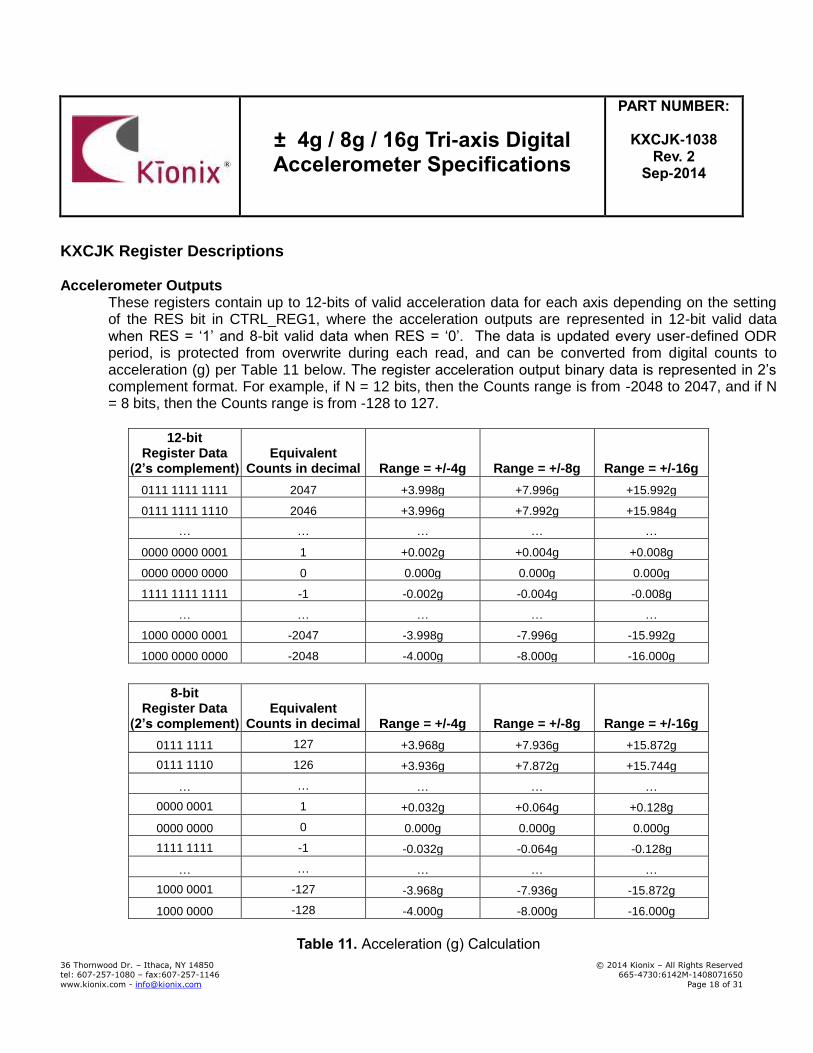
KXCJK Register Descriptions Accelerometer Outputs
These registers contain up to 12-bits of valid acceleration data for each axis depending on the setting of the RES bit in CTRL_REG1, where the acceleration outputs are represented in 12-bit valid data when RES = ‘1’ and 8-bit valid data when RES = ‘0’. The data is updated every user-defined ODR period, is protected from overwrite during each read, and can be converted from digital counts to acceleration (g) per Table 11 below. The register acceleration output binary data is represented in 2’s complement format. For example, if N = 12 bits, then the Counts range is from -2048 to 2047, and if N = 8 bits, then the Counts range is from -128 to 127.
12-bit
Register Data (2’s complement)
Equivalent Counts in decimal Range = +/-4g Range = +/-8g Range = +/-16g
0111 1111 1111 2047 +3.998g +7.996g +15.992g
0111 1111 1110 2046 +3.996g +7.992g +15.984g
… … … … …
0000 0000 0001 1 +0.002g +0.004g +0.008g
0000 0000 0000 0 0.000g 0.000g 0.000g
1111 1111 1111 -1 -0.002g -0.004g -0.008g
… … … … …
1000 0000 0001 -2047 -3.998g -7.996g -15.992g
1000 0000 0000 -2048 -4.000g -8.000g -16.000g
8-bit
Register Data (2’s complement)
Equivalent
Counts in decimal Range = +/-4g Range = +/-8g Range = +/-16g
0111 1111 127 +3.968g +7.936g +15.872g
0111 1110 126 +3.936g +7.872g +15.744g
… … … … …
0000 0001 1 +0.032g +0.064g +0.128g
0000 0000 0 0.000g 0.000g 0.000g
1111 1111 -1 -0.032g -0.064g -0.128g
… … … … …
1000 0001 -127 -3.968g -7.936g -15.872g
1000 0000 -128 -4.000g -8.000g -16.000g
Table 11. Acceleration (g) Calculation
± 4g / 8g / 16g Tri-axis Digital Accelerometer Specifications
PART NUMBER:
KXCJK-1038 Rev. 2
Sep-2014
36 Thornwood Dr. – Ithaca, NY 14850 © 2014 Kionix – All Rights Reserved tel: 607-257-1080 – fax:607-257-1146 665-4730:6142M-1408071650
www.kionix.com - [email protected] Page 19 of 31
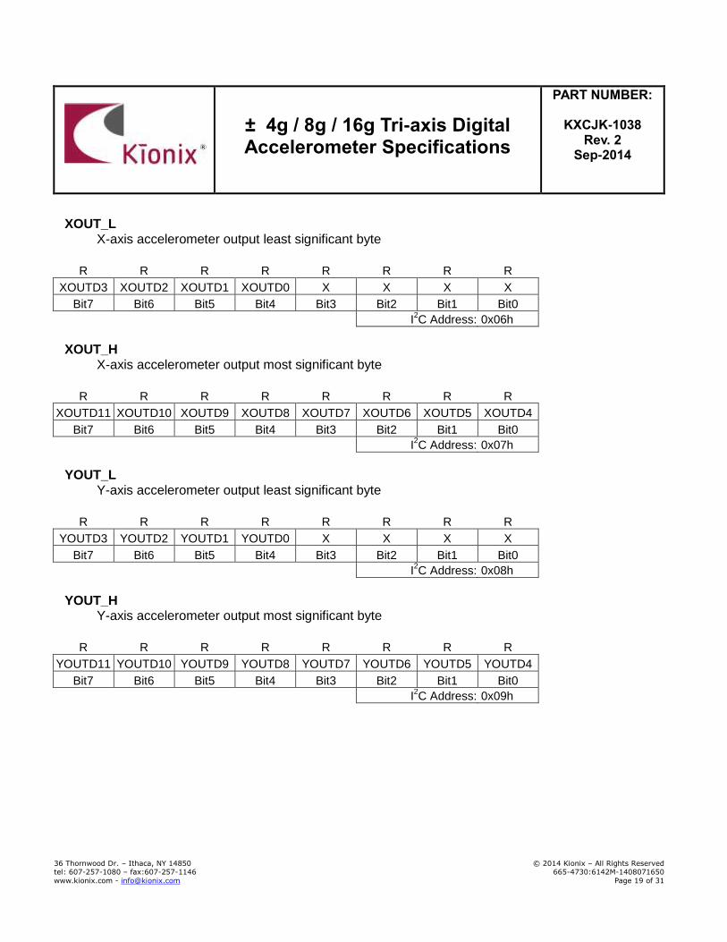
XOUT_L X-axis accelerometer output least significant byte
R R R R R R R R
XOUTD3 XOUTD2 XOUTD1 XOUTD0 X X X X
Bit7 Bit6 Bit5 Bit4 Bit3 Bit2 Bit1 Bit0
I2C Address: 0x06h
XOUT_H
X-axis accelerometer output most significant byte
R R R R R R R R
XOUTD11 XOUTD10 XOUTD9 XOUTD8 XOUTD7 XOUTD6 XOUTD5 XOUTD4
Bit7 Bit6 Bit5 Bit4 Bit3 Bit2 Bit1 Bit0
I2C Address: 0x07h
YOUT_L
Y-axis accelerometer output least significant byte
R R R R R R R R
YOUTD3 YOUTD2 YOUTD1 YOUTD0 X X X X
Bit7 Bit6 Bit5 Bit4 Bit3 Bit2 Bit1 Bit0
I2C Address: 0x08h
YOUT_H
Y-axis accelerometer output most significant byte
R R R R R R R R
YOUTD11 YOUTD10 YOUTD9 YOUTD8 YOUTD7 YOUTD6 YOUTD5 YOUTD4
Bit7 Bit6 Bit5 Bit4 Bit3 Bit2 Bit1 Bit0
I2C Address: 0x09h
± 4g / 8g / 16g Tri-axis Digital Accelerometer Specifications
PART NUMBER:
KXCJK-1038 Rev. 2
Sep-2014
36 Thornwood Dr. – Ithaca, NY 14850 © 2014 Kionix – All Rights Reserved tel: 607-257-1080 – fax:607-257-1146 665-4730:6142M-1408071650
www.kionix.com - [email protected] Page 20 of 31
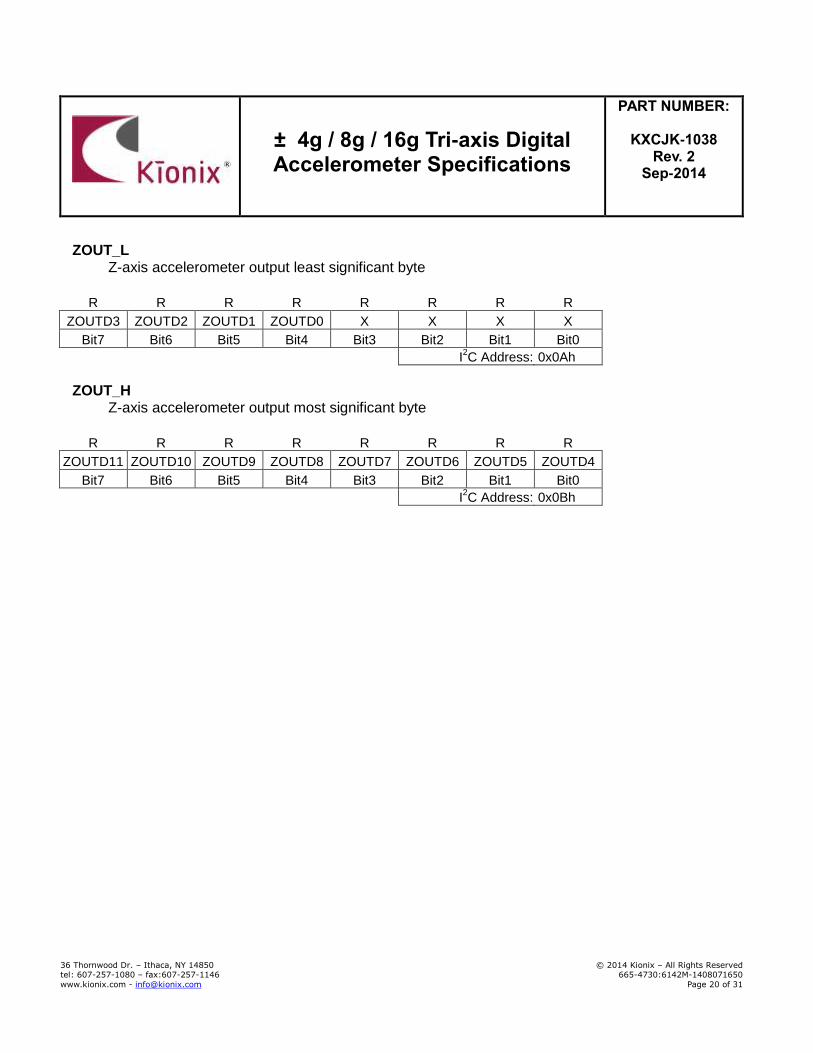
ZOUT_L Z-axis accelerometer output least significant byte
R R R R R R R R
ZOUTD3 ZOUTD2 ZOUTD1 ZOUTD0 X X X X
Bit7 Bit6 Bit5 Bit4 Bit3 Bit2 Bit1 Bit0
I2C Address: 0x0Ah
ZOUT_H
Z-axis accelerometer output most significant byte
R R R R R R R R
ZOUTD11 ZOUTD10 ZOUTD9 ZOUTD8 ZOUTD7 ZOUTD6 ZOUTD5 ZOUTD4
Bit7 Bit6 Bit5 Bit4 Bit3 Bit2 Bit1 Bit0
I2C Address: 0x0Bh
± 4g / 8g / 16g Tri-axis Digital Accelerometer Specifications
PART NUMBER:
KXCJK-1038 Rev. 2
Sep-2014
36 Thornwood Dr. – Ithaca, NY 14850 © 2014 Kionix – All Rights Reserved tel: 607-257-1080 – fax:607-257-1146 665-4730:6142M-1408071650
www.kionix.com - [email protected] Page 21 of 31
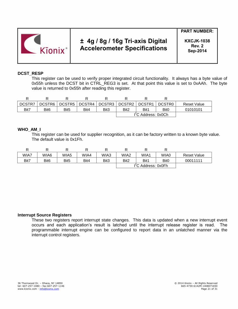
DCST_RESP This register can be used to verify proper integrated circuit functionality. It always has a byte value of 0x55h unless the DCST bit in CTRL_REG3 is set. At that point this value is set to 0xAAh. The byte value is returned to 0x55h after reading this register.
R R R R R R R R
DCSTR7 DCSTR6 DCSTR5 DCSTR4 DCSTR3 DCSTR2 DCSTR1 DCSTR0 Reset Value
Bit7 Bit6 Bit5 Bit4 Bit3 Bit2 Bit1 Bit0 01010101
I2C Address: 0x0Ch
WHO_AM_I This register can be used for supplier recognition, as it can be factory written to a known byte value. The default value is 0x1Fh.
R R R R R R R R
WIA7 WIA6 WIA5 WIA4 WIA3 WIA2 WIA1 WIA0 Reset Value
Bit7 Bit6 Bit5 Bit4 Bit3 Bit2 Bit1 Bit0 00011111
I2C Address: 0x0Fh
Interrupt Source Registers
These two registers report interrupt state changes. This data is updated when a new interrupt event occurs and each application’s result is latched until the interrupt release register is read. The programmable interrupt engine can be configured to report data in an unlatched manner via the interrupt control registers.
± 4g / 8g / 16g Tri-axis Digital Accelerometer Specifications
PART NUMBER:
KXCJK-1038 Rev. 2
Sep-2014
36 Thornwood Dr. – Ithaca, NY 14850 © 2014 Kionix – All Rights Reserved tel: 607-257-1080 – fax:607-257-1146 665-4730:6142M-1408071650
www.kionix.com - [email protected] Page 22 of 31
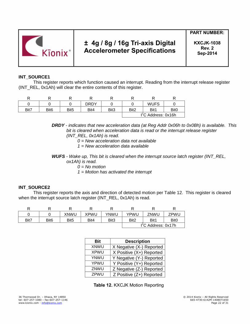
INT_SOURCE1 This register reports which function caused an interrupt. Reading from the interrupt release register (INT_REL, 0x1Ah) will clear the entire contents of this register.
R R R R R R R R
0 0 0 DRDY 0 0 WUFS 0
Bit7 Bit6 Bit5 Bit4 Bit3 Bit2 Bit1 Bit0
I2C Address: 0x16h
DRDY - indicates that new acceleration data (at Reg Addr 0x06h to 0x0Bh) is available. This
bit is cleared when acceleration data is read or the interrupt release register (INT_REL, 0x1Ah) is read.
0 = New acceleration data not available 1 = New acceleration data available WUFS - Wake up, This bit is cleared when the interrupt source latch register (INT_REL,
ox1Ah) is read. 0 = No motion 1 = Motion has activated the interrupt
INT_SOURCE2 This register reports the axis and direction of detected motion per Table 12. This register is cleared when the interrupt source latch register (INT_REL, 0x1Ah) is read.
R R R R R R R R
0 0 XNWU XPWU YNWU YPWU ZNWU ZPWU
Bit7 Bit6 Bit5 Bit4 Bit3 Bit2 Bit1 Bit0
I2C Address: 0x17h
Bit Description XNWU X Negative (X-) Reported XPWU X Positive (X+) Reported YNWU Y Negative (Y-) Reported YPWU Y Positive (Y+) Reported ZNWU Z Negative (Z-) Reported ZPWU Z Positive (Z+) Reported
Table 12. KXCJK Motion Reporting
± 4g / 8g / 16g Tri-axis Digital Accelerometer Specifications
PART NUMBER:
KXCJK-1038 Rev. 2
Sep-2014
36 Thornwood Dr. – Ithaca, NY 14850 © 2014 Kionix – All Rights Reserved tel: 607-257-1080 – fax:607-257-1146 665-4730:6142M-1408071650
www.kionix.com - [email protected] Page 23 of 31
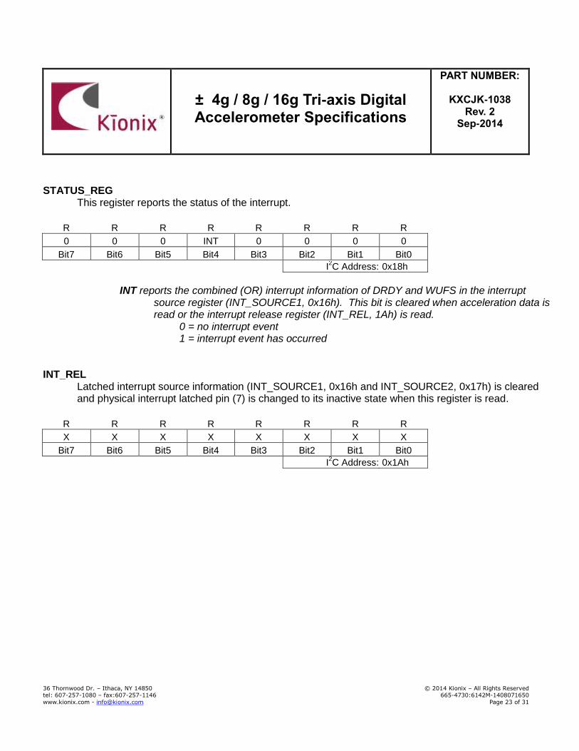
STATUS_REG This register reports the status of the interrupt.
R R R R R R R R
0 0 0 INT 0 0 0 0
Bit7 Bit6 Bit5 Bit4 Bit3 Bit2 Bit1 Bit0
I2C Address: 0x18h
INT reports the combined (OR) interrupt information of DRDY and WUFS in the interrupt
source register (INT_SOURCE1, 0x16h). This bit is cleared when acceleration data is read or the interrupt release register (INT_REL, 1Ah) is read.
0 = no interrupt event 1 = interrupt event has occurred
INT_REL
Latched interrupt source information (INT_SOURCE1, 0x16h and INT_SOURCE2, 0x17h) is cleared and physical interrupt latched pin (7) is changed to its inactive state when this register is read.
R R R R R R R R
X X X X X X X X
Bit7 Bit6 Bit5 Bit4 Bit3 Bit2 Bit1 Bit0
I2C Address: 0x1Ah
± 4g / 8g / 16g Tri-axis Digital Accelerometer Specifications
PART NUMBER:
KXCJK-1038 Rev. 2
Sep-2014
36 Thornwood Dr. – Ithaca, NY 14850 © 2014 Kionix – All Rights Reserved tel: 607-257-1080 – fax:607-257-1146 665-4730:6142M-1408071650
www.kionix.com - [email protected] Page 24 of 31
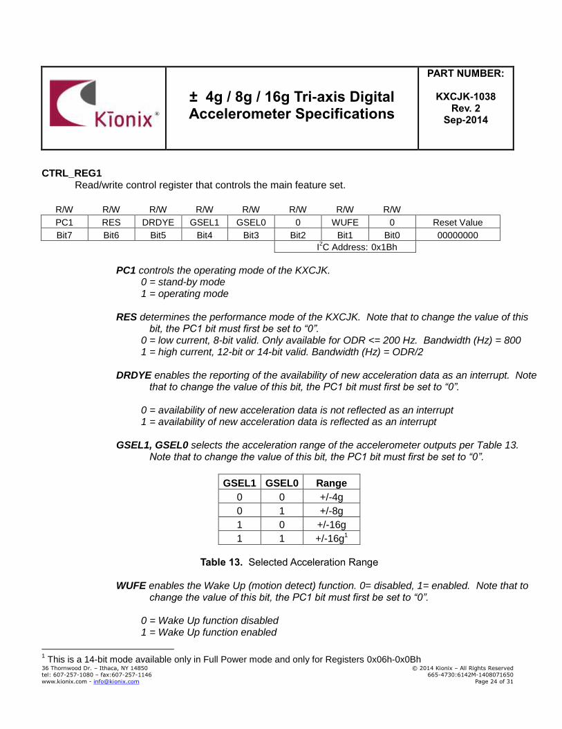
CTRL_REG1 Read/write control register that controls the main feature set.
R/W R/W R/W R/W R/W R/W R/W R/W
PC1 RES DRDYE GSEL1 GSEL0 0 WUFE 0 Reset Value
Bit7 Bit6 Bit5 Bit4 Bit3 Bit2 Bit1 Bit0 00000000
I2C Address: 0x1Bh
PC1 controls the operating mode of the KXCJK.
0 = stand-by mode 1 = operating mode
RES determines the performance mode of the KXCJK. Note that to change the value of this bit, the PC1 bit must first be set to “0”.
0 = low current, 8-bit valid. Only available for ODR <= 200 Hz. Bandwidth (Hz) = 800 1 = high current, 12-bit or 14-bit valid. Bandwidth (Hz) = ODR/2
DRDYE enables the reporting of the availability of new acceleration data as an interrupt. Note
that to change the value of this bit, the PC1 bit must first be set to “0”.
0 = availability of new acceleration data is not reflected as an interrupt 1 = availability of new acceleration data is reflected as an interrupt
GSEL1, GSEL0 selects the acceleration range of the accelerometer outputs per Table 13. Note that to change the value of this bit, the PC1 bit must first be set to “0”.
GSEL1 GSEL0 Range
0 0 +/-4g
0 1 +/-8g
1 0 +/-16g
1 1 +/-16g1
Table 13. Selected Acceleration Range
WUFE enables the Wake Up (motion detect) function. 0= disabled, 1= enabled. Note that to
change the value of this bit, the PC1 bit must first be set to “0”.
0 = Wake Up function disabled 1 = Wake Up function enabled
1 This is a 14-bit mode available only in Full Power mode and only for Registers 0x06h-0x0Bh
± 4g / 8g / 16g Tri-axis Digital Accelerometer Specifications
PART NUMBER:
KXCJK-1038 Rev. 2
Sep-2014
36 Thornwood Dr. – Ithaca, NY 14850 © 2014 Kionix – All Rights Reserved tel: 607-257-1080 – fax:607-257-1146 665-4730:6142M-1408071650
www.kionix.com - [email protected] Page 25 of 31
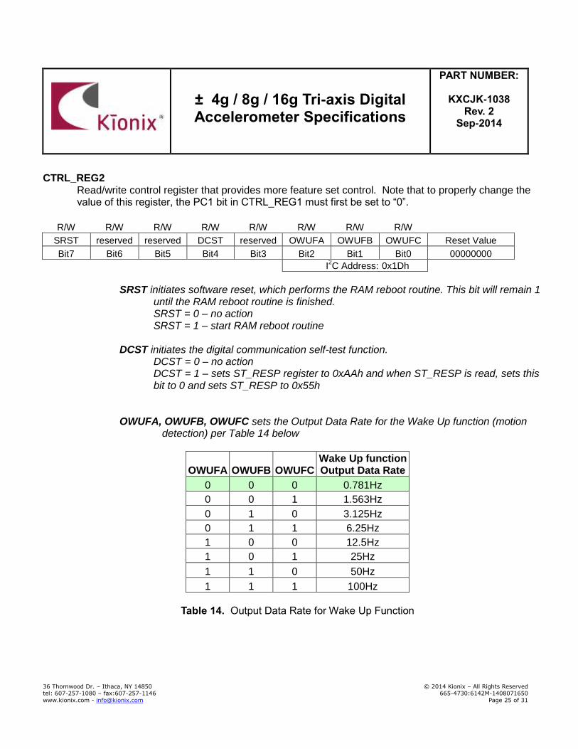
CTRL_REG2 Read/write control register that provides more feature set control. Note that to properly change the value of this register, the PC1 bit in CTRL_REG1 must first be set to “0”.
R/W R/W R/W R/W R/W R/W R/W R/W
SRST reserved reserved DCST reserved OWUFA OWUFB OWUFC Reset Value
Bit7 Bit6 Bit5 Bit4 Bit3 Bit2 Bit1 Bit0 00000000
I2C Address: 0x1Dh
SRST initiates software reset, which performs the RAM reboot routine. This bit will remain 1
until the RAM reboot routine is finished. SRST = 0 – no action SRST = 1 – start RAM reboot routine
DCST initiates the digital communication self-test function. DCST = 0 – no action DCST = 1 – sets ST_RESP register to 0xAAh and when ST_RESP is read, sets this
bit to 0 and sets ST_RESP to 0x55h OWUFA, OWUFB, OWUFC sets the Output Data Rate for the Wake Up function (motion
detection) per Table 14 below
OWUFA OWUFB OWUFC Wake Up function Output Data Rate
0 0 0 0.781Hz
0 0 1 1.563Hz
0 1 0 3.125Hz
0 1 1 6.25Hz
1 0 0 12.5Hz
1 0 1 25Hz
1 1 0 50Hz
1 1 1 100Hz
Table 14. Output Data Rate for Wake Up Function
± 4g / 8g / 16g Tri-axis Digital Accelerometer Specifications
PART NUMBER:
KXCJK-1038 Rev. 2
Sep-2014
36 Thornwood Dr. – Ithaca, NY 14850 © 2014 Kionix – All Rights Reserved tel: 607-257-1080 – fax:607-257-1146 665-4730:6142M-1408071650
www.kionix.com - [email protected] Page 26 of 31
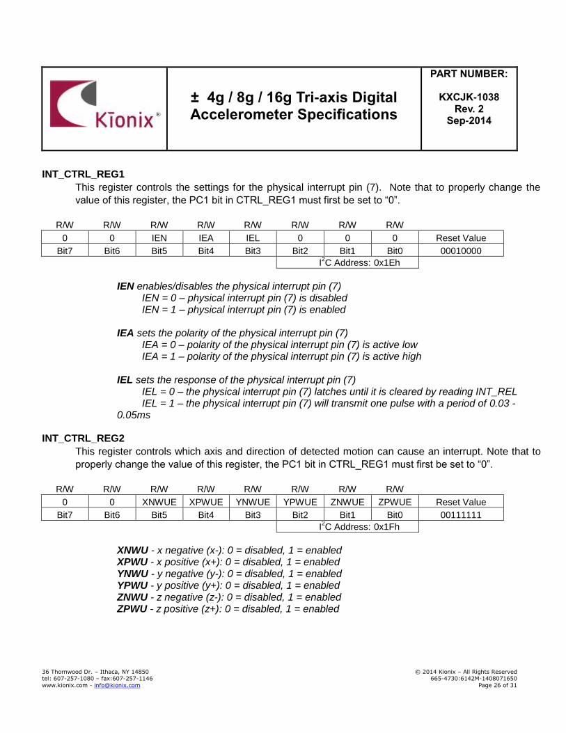
INT_CTRL_REG1
This register controls the settings for the physical interrupt pin (7). Note that to properly change the
value of this register, the PC1 bit in CTRL_REG1 must first be set to “0”.
R/W R/W R/W R/W R/W R/W R/W R/W
0 0 IEN IEA IEL 0 0 0 Reset Value
Bit7 Bit6 Bit5 Bit4 Bit3 Bit2 Bit1 Bit0 00010000
I2C Address: 0x1Eh
IEN enables/disables the physical interrupt pin (7) IEN = 0 – physical interrupt pin (7) is disabled IEN = 1 – physical interrupt pin (7) is enabled IEA sets the polarity of the physical interrupt pin (7) IEA = 0 – polarity of the physical interrupt pin (7) is active low IEA = 1 – polarity of the physical interrupt pin (7) is active high IEL sets the response of the physical interrupt pin (7) IEL = 0 – the physical interrupt pin (7) latches until it is cleared by reading INT_REL IEL = 1 – the physical interrupt pin (7) will transmit one pulse with a period of 0.03 -
0.05ms
INT_CTRL_REG2
This register controls which axis and direction of detected motion can cause an interrupt. Note that to
properly change the value of this register, the PC1 bit in CTRL_REG1 must first be set to “0”.
R/W R/W R/W R/W R/W R/W R/W R/W
0 0 XNWUE XPWUE YNWUE YPWUE ZNWUE ZPWUE Reset Value
Bit7 Bit6 Bit5 Bit4 Bit3 Bit2 Bit1 Bit0 00111111
I2C Address: 0x1Fh
XNWU - x negative (x-): 0 = disabled, 1 = enabled XPWU - x positive (x+): 0 = disabled, 1 = enabled YNWU - y negative (y-): 0 = disabled, 1 = enabled YPWU - y positive (y+): 0 = disabled, 1 = enabled ZNWU - z negative (z-): 0 = disabled, 1 = enabled ZPWU - z positive (z+): 0 = disabled, 1 = enabled
± 4g / 8g / 16g Tri-axis Digital Accelerometer Specifications
PART NUMBER:
KXCJK-1038 Rev. 2
Sep-2014
36 Thornwood Dr. – Ithaca, NY 14850 © 2014 Kionix – All Rights Reserved tel: 607-257-1080 – fax:607-257-1146 665-4730:6142M-1408071650
www.kionix.com - [email protected] Page 27 of 31
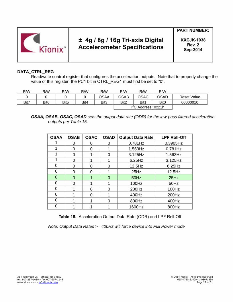
DATA_CTRL_REG Read/write control register that configures the acceleration outputs. Note that to properly change the value of this register, the PC1 bit in CTRL_REG1 must first be set to “0”.
R/W R/W R/W R/W R/W R/W R/W R/W
0 0 0 0 OSAA OSAB OSAC OSAD Reset Value
Bit7 Bit6 Bit5 Bit4 Bit3 Bit2 Bit1 Bit0 00000010
I2C Address: 0x21h
OSAA, OSAB, OSAC, OSAD sets the output data rate (ODR) for the low-pass filtered acceleration
outputs per Table 15.
OSAA OSAB OSAC OSAD Output Data Rate LPF Roll-Off
1 0 0 0 0.781Hz 0.3905Hz
1 0 0 1 1.563Hz 0.781Hz
1 0 1 0 3.125Hz 1.563Hz
1 0 1 1 6.25Hz 3.125Hz
0 0 0 0 12.5Hz 6.25Hz
0 0 0 1 25Hz 12.5Hz
0 0 1 0 50Hz 25Hz
0 0 1 1 100Hz 50Hz
0 1 0 0 200Hz 100Hz
0 1 0 1 400Hz 200Hz
0 1 1 0 800Hz 400Hz
0 1 1 1 1600Hz 800Hz
Table 15. Acceleration Output Data Rate (ODR) and LPF Roll-Off
Note: Output Data Rates >= 400Hz will force device into Full Power mode
± 4g / 8g / 16g Tri-axis Digital Accelerometer Specifications
PART NUMBER:
KXCJK-1038 Rev. 2
Sep-2014
36 Thornwood Dr. – Ithaca, NY 14850 © 2014 Kionix – All Rights Reserved tel: 607-257-1080 – fax:607-257-1146 665-4730:6142M-1408071650
www.kionix.com - [email protected] Page 28 of 31
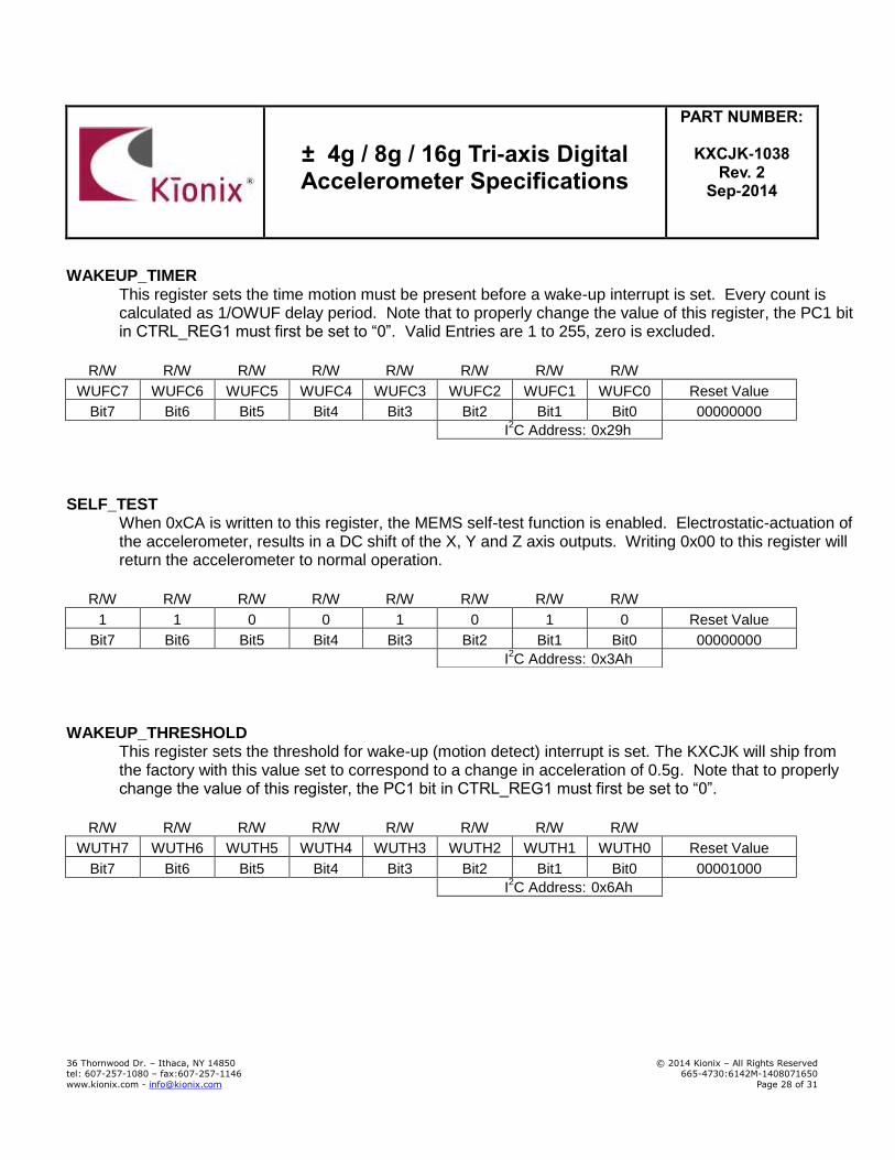
WAKEUP_TIMER This register sets the time motion must be present before a wake-up interrupt is set. Every count is calculated as 1/OWUF delay period. Note that to properly change the value of this register, the PC1 bit in CTRL_REG1 must first be set to “0”. Valid Entries are 1 to 255, zero is excluded.
R/W R/W R/W R/W R/W R/W R/W R/W
WUFC7 WUFC6 WUFC5 WUFC4 WUFC3 WUFC2 WUFC1 WUFC0 Reset Value
Bit7 Bit6 Bit5 Bit4 Bit3 Bit2 Bit1 Bit0 00000000
I2C Address: 0x29h
SELF_TEST
When 0xCA is written to this register, the MEMS self-test function is enabled. Electrostatic-actuation of the accelerometer, results in a DC shift of the X, Y and Z axis outputs. Writing 0x00 to this register will return the accelerometer to normal operation.
WAKEUP_THRESHOLD
This register sets the threshold for wake-up (motion detect) interrupt is set. The KXCJK will ship from the factory with this value set to correspond to a change in acceleration of 0.5g. Note that to properly change the value of this register, the PC1 bit in CTRL_REG1 must first be set to “0”.
R/W R/W R/W R/W R/W R/W R/W R/W
WUTH7 WUTH6 WUTH5 WUTH4 WUTH3 WUTH2 WUTH1 WUTH0 Reset Value
Bit7 Bit6 Bit5 Bit4 Bit3 Bit2 Bit1 Bit0 00001000
I2C Address: 0x6Ah
R/W R/W R/W R/W R/W R/W R/W R/W
1 1 0 0 1 0 1 0 Reset Value
Bit7 Bit6 Bit5 Bit4 Bit3 Bit2 Bit1 Bit0 00000000
I2C Address: 0x3Ah

± 4g / 8g / 16g Tri-axis Digital Accelerometer Specifications
PART NUMBER:
KXCJK-1038 Rev. 2
Sep-2014
36 Thornwood Dr. – Ithaca, NY 14850 © 2014 Kionix – All Rights Reserved tel: 607-257-1080 – fax:607-257-1146 665-4730:6142M-1408071650
www.kionix.com - [email protected] Page 29 of 31
KXCJK Embedded Wake Up Function The KXCJK contains an interrupt engine that can be configured by the user to report when qualified changes in acceleration occur. The user has the option to enable or disable specific axes and specific directions, as well as to specify the delay time. An example use case for the engine would be to detect motion on any axis to signal an event and wake up the accelerometer or other devices. This can be achieved by configuring the engine to detect when the acceleration on any axis is greater than the user-defined threshold for a user-defined amount of time. Equations 1 and 2 show how to calculate the engine threshold (WAKEUP_THRESHOLD) and delay time (WAKEUP_TIMER) register values for the desired result.
WAKEUP_THRESHOLD (counts) = Desired Threshold (g) x 8 (counts/g)
Equation 1. Wake Up Threshold
WAKEUP_TIMER (counts) = Desired Delay Time (sec) x OWUF (Hz)
Equation 2. Wake Up Delay Time
± 4g / 8g / 16g Tri-axis Digital Accelerometer Specifications
PART NUMBER:
KXCJK-1038 Rev. 2
Sep-2014
36 Thornwood Dr. – Ithaca, NY 14850 © 2014 Kionix – All Rights Reserved tel: 607-257-1080 – fax:607-257-1146 665-4730:6142M-1408071650
www.kionix.com - [email protected] Page 30 of 31
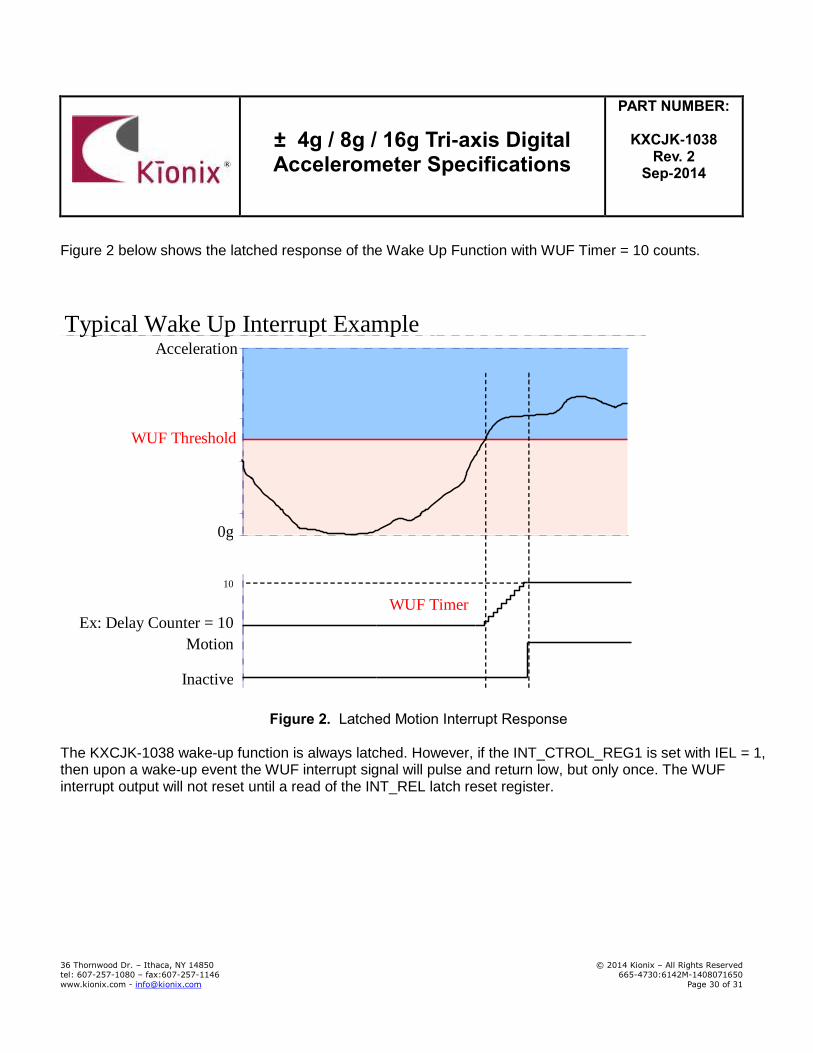
Figure 2 below shows the latched response of the Wake Up Function with WUF Timer = 10 counts.
0g
Typical Wake Up Interrupt Example Acceleration
WUF Threshold
Ex: Delay Counter = 10
Motion
10
Inactive
WUF Timer
Figure 2. Latched Motion Interrupt Response
The KXCJK-1038 wake-up function is always latched. However, if the INT_CTROL_REG1 is set with IEL = 1, then upon a wake-up event the WUF interrupt signal will pulse and return low, but only once. The WUF interrupt output will not reset until a read of the INT_REL latch reset register.
± 4g / 8g / 16g Tri-axis Digital Accelerometer Specifications
PART NUMBER:
KXCJK-1038 Rev. 2
Sep-2014
36 Thornwood Dr. – Ithaca, NY 14850 © 2014 Kionix – All Rights Reserved tel: 607-257-1080 – fax:607-257-1146 665-4730:6142M-1408071650
www.kionix.com - [email protected] Page 31 of 31
Revision History
REVISION DESCRIPTION DATE
1 Initial Release 07-Aug-2014
2 revised WHO_AM_I value 12-Sep-2014
"Kionix" is a registered trademark of Kionix, Inc. Products described herein are protected by patents issued or pending. No license is granted by implication or otherwise under any patent or other rights of Kionix. The information contained herein is believed to be accurate and reliable but is not guaranteed. Kionix does not assume responsibility for its use or distribution. Kionix also reserves the right to change product specifications or discontinue this product at any time without prior notice. This publication supersedes and replaces all information previously supplied.