© 2010 Chao-Hsin Wu - Illinois: IDEALS Home
86
© 2010 Chao-Hsin Wu
Transcript of © 2010 Chao-Hsin Wu - Illinois: IDEALS Home

© 2010 Chao-Hsin Wu

DESIGN, FABRICATION, AND CHARACTERIZATION OF HIGH-SPEED LIGHT-EMITTING TRANSISTORS AND MICROCAVITY
LASERS
BY
CHAO-HSIN WU
DISSERTATION
Submitted in partial fulfillment of the requirements for the degree of Doctor of Philosophy in Electrical and Computer Engineering
in the Graduate College of the University of Illinois at Urbana-Champaign, 2010
Urbana, Illinois
Doctoral Committee: Professor Milton Feng, Chair and Director of Research Professor Nick Holonyak, Jr. Adjunct Professor Keh-Yung Cheng Adjunct Professor Kuang-Chien Hsieh Professor Jianming Jin

ii
ABSTRACT
Carrier spontaneous recombination lifetime has been thought to be limited to
~ 1 ns in light-emitting diodes and diode lasers for the past forty years. In the present
work the recombination lifetime demonstrated is able to be “tailored” (reduced) by the
provided material system, cavity size, and layout design. In a light-emitting transistor or
tilted-charge light-emitting diode, the effective carrier recombination lifetime can be
readily reduced to 23 ps (spontaneous modulation bandwidth f-3dB = 7 GHz) by
employing un-doped quantum wells in the highly-doped thin base region and allowing
only “fast” recombining carriers to recombine through a reverse-biased base-collector
junction boundary condition. A light-emitting transistor possesses, in addition, a unique
three-terminal electrical-optical characteristic potentially leading to advantageous and
useful features for high-speed short-range optical transmitters and interconnects. It has
been shown that a microcavity vertical-cavity surface-emitting laser employing small
aperture buried-oxide current and field confinement is also demonstrated with wider
mode spacing and faster carrier recombination lifetime (enhanced Purcell factor ~ 2 to 8
times, but still limited cavity), lower threshold current, larger side mode suppression ratio,
and higher photon density and temperature insensitivity.

iii
To My Family

iv
ACKNOWLEDGMENTS I wish to show my greatest thanks to Professor Milton Feng for the opportunity to
work on the light-emitting transistor and transistor laser project in the University of
Illinois at Urbana-Champaign. His advice, direction, and attitude have inspired me and
led me to a new page. I am very grateful to Professor Nick Holonyak Jr. for his generous
ideas, guidance, and philosophy. From him I see a grand virtue of a truly successful
pioneer, and contributor in semiconductor history. I also want to thank Dr. Gabriel
Walter for his helping hand with training from the beginning. Through our discussions, I
have been able to learn and try out new ideas. Many thanks also go to Professor K. Y.
Cheng, Professor K. C. Hsieh and Professor Jianming Jin for serving on my preliminary
and final examination committees and for their support. Special thanks to Dr. Benjamin
Chu-Kung, Dr. Han Wui Then and Mr. Donald Kuang-Yu Cheng for their selfless
instruction, discussion, help, company, and support during my graduate research life in
Illinois. I would like to mention the help from HSIC members past and present: Dr.
Richard Chan, Dr. William Snodgrass, Dr. Doris Chen, Dr. Adam James, Dr. Forest
Dixon, Dr. Giang Nguyen, Mr. Mark Stuenkel, Mr. Mong-Kai Wu, Mr. Fei Tan, Mr.
Rohan Bambery, Mr. Eric Iverson, and Mr. Huiming Xu. Without their help and support,
none of the work documented here would have been possible. Finally I am very grateful
to my dear family members, Dr. Ching-Ji Wu, Mrs. Shu-Mei Liu, Deirdra Wu, and
Daniella Wu, for always staying there for me.

v
TABLE OF CONTENTS 1. INTRODUCTION ....................................................................................................... 1
1.1. Outline of Problem.............................................................................................. 2 1.2. Organization of Work ......................................................................................... 2
2. TOWARD MULTI-GHZ OPERATION LIGHT-EMITTING TRANSISTORS........ 6
2.1. Three-Port DC and RF Characteristics ............................................................... 6 2.2. Lateral Scaling Toward GHz Operation ........................................................... 10 2.3. Figures............................................................................................................... 15
3. DESIGN OF MULTI-GHZ TILTED-CHARGE LIGHT-EMITTING DIODES ..... 20
3.1. Theory and Characterization of Tilted-Charge LED ........................................ 20 3.2. 4 GHz 2x2 Integrated LED Array..................................................................... 24 3.3. Figures............................................................................................................... 27
4. MICROCAVITY QUANTUM-WELL VERTICAL CAVITY SURFACE-
EMITTING LASERS ................................................................................................ 32 4.1. Microwave Characterization of Purcell Enhancement ..................................... 32 4.2. Microwave Determination of Electron-Hole Recombination Dynamics from
Spontaneous to Stimulated Emission................................................................ 38 4.3. Table and Figures.............................................................................................. 44
5. THE EFFECT OF MICROCAVITY LASER RECOMBINATION LIFETIME
ON MICROWAVE BANDWIDTH AND EYE-DIAGRAM SIGNAL INTEGRITY………………………………………………………………………...50 5.1 Spectral Mode Spacing and Purcell Effect ....................................................... 51 5.2 Temperature Insensitive Characteristics ........................................................... 56 5.3 Microwave Bandwidth and Eye-Diagram Signal Integrity .............................. 58 5.4 Microwave Small-Signal Model ....................................................................... 63 5.5 Tables and Figures............................................................................................ 68
6. CONCLUSION............................................................................................................ 75
REFERENCES ................................................................................................................. 78

1
1. INTRODUCTION
Semiconductor light-emitting diodes (LEDs) using direct gap III-V materials, and
electron-hole injection and recombination,1-4 have over the years led to numerous
applications in display and lightwave communications. Fast spontaneous lightwave
transmitters can be an attractive solution for short range optical data communications and
optical interconnections as their threshold-less operation, high fabrication yield and
reduced complexity of driver and need for threshold feedback control are reduced
significantly, thus reducing the overall cost, form-factor and power consumption of
transmitters. Coupled with a proper cavity design, such as a resonant cavity, spontaneous
light sources emitting at 980 nm have been shown to achieve external quantum
efficiencies (ext) as high as 27% and an emission spectral width as narrow as 5 nm.5
However, the fastest spontaneous light source shown to date (a light-emitting diode)
employs p-doping as high as 7x1019 cm-3 to achieve a bandwidth of 1.7 GHz (i.e.,
recombination lifetime of ~ 100 ps), at the cost of a reduced internal quantum efficiency
to 10% or less.6 In practice, higher efficiency spontaneous devices such as LEDs or
RCLEDs operate with bandwidths that are less than 1 GHz, restricting actual commercial
application of spontaneous light transmitters (LEDs and RCLEDs) to less than 1 Gbits/s.
Earlier, we have proposed that the heterojunction bipolar light-emitting transistor
(HBLET),7,8 which utilizes a high-speed heterojunction bipolar transistor (HBT)
structure,9 could potentially function as a light source with speeds exceeding tens of GHz.
The room temperature, continuous wave operation of a transistor laser (TL) further
demonstrates that a practical radiative recombination center (i.e., undoped quantum well)
can be incorporated in the heavily doped base region of a HBLET.10, 11, 12 The TL is

2
capable of achieving a modulation bandwidth of 13.5 GHz (despite a large cavity length
of 400 m) or even more, and absence of resonance frequency.13
1.1. Outline of Problem
Due to the short base effect of tilted charge population in transistors, the effective
minority carrier lifetime in the base region of the HBLETs can be progressively reduced
to sub-100 ps by tailoring the doping and incorporating QW(s).14 In the high-speed
modulation of an HBLET, the extrinsic parasitic capacitive charging delay due to lateral
extrinsic carrier transport effects ultimately limits the maximum optical bandwidth
achievable and must therefore be taken into account. In practice, despite the high
intrinsic speed of the HBT, the microwave performance of an HBLET is severely limited
by parasitic capacitances, partly owing to the need to include light extraction features
(such as oxide apertures) not present in traditional high-speed HBT devices. To reduce
the parasitics, scaling effect will need to be reviewed during the design of improved light-
emitting source. The characteristics of the HBLET can be understood by the microwave
electrical and optical analysis of different layout design in order to provide the necessary
information leading to the next stage—vertical cavity transistor lasers (VCTL).
1.2. Organization of Work The organization of the thesis proposal is as follows:
In Chapter 2, we demonstrate a quantum-well base heterojunction bipolar light-
emitting transistor (HBLET) operating in the common collector configuration with a 3 dB
optical response bandwidth f-3dB of 4.3 GHz. The HBLET has a current gain, (=
|IC/IB| ) as high as 30, and can be operated as a three-port device to provide

3
simultaneously an optical and electrical output with gain. The f3dB of 4.3 GHz
corresponds to an effective carrier recombination lifetime of 37 ps, and shows that “fast”
spontaneous recombination can be harnessed for high-speed modulation. In the high-
speed modulation of an HBLET, the extrinsic parasitic capacitive charging delay due to
lateral extrinsic carrier transport effects ultimately limits the maximum optical bandwidth
achievable and must therefore be taken into account. In the present work, we verify this
by showing that the extrinsic-parasitic-limitations on the recombination lifetime can be
reduced sufficiently to give B < 100 ps by laterally scaling the emitter aperture width
from 13 m to 5 m to reduce the extrinsic capacitive charging and simultaneously
increase the current density. This work has resulted in the record performance of
spontaneous optical modulation bandwidth as high as 4.3 GHz for a 5 m emitter
aperture HBLET.
In Chapter 3, we demonstrate a higher speed form of light-emitting diode (LED), an
asymmetrical two-junction tilted-charge LED, utilizing an n-type buried “drain” layer
beneath the p-type “base” quantum-well (carrier and photon) active region. The “drain”
layer tilts and pins the charge in the manner of a heterojunction bipolar light-emitting
transistor (HBLET), selecting and allowing only “fast” recombination (recombination
lifetime, B, of the order of “base” transit time, t). The tilted-charge LED, simple in
design and construction, is capable of operation at low current in spontaneous
recombination at a 7 GHz bandwidth or even higher with more refinement. We also
demonstrate a 4.3 GHz high-speed tilted-charge integrated 2 x 2 LED array. With an
array of four LEDs operating in parallel, the optical output power can be as much as
tripled while the peak high-speed performance of its individual LED component is

4
preserved. The gigahertz bandwidth is achieved by utilizing a “drain” layer, common to
all the devices in the array, to enforce a “tilted-charge” condition where only fast
recombination is employed for the modulation of optical output. The successful
integration of four “tilted-charge” LEDs in a parallel array paves the way towards a
simple viable solution for ultra-high-speed short range optical communication.
After having discussed the high speed operation of HBLET and tilted-charge LED,
in Chapter 4, the microwave characteristics of a microcavity vertical-cavity surface
light-emitting laser (VCSEL) incorporated with small oxide-confined aperture is
presented. A sensitive microwave method is described to study the optical frequency
response of a microcavity laser, demonstrating that a quantum-well VCSEL (~ 3 m
aperture, ITH = 180 A) can exhibit almost single-mode operation (nearly threshold
free), and an electron-hole spontaneous lifetime Purcell enhancement of 2.08 times.
The microwave-measurement method employing electrical-to-optical conversion, and
distinct separation of electrical input and optical output, is more revealing than
photoluminescence decay experiments (and the inconvenient overlap of optical input
and output). By studying the optical microwave frequency response of a microcavity
quantum-well VCSEL in the transition, over a low (a spread-out) mode density, from
spontaneous to coherent operation, we resolve the dynamics (spontaneous to stimulated)
of electron-hole recombination and reveal the existence of “fast” spontaneous
recombination (Bspon < 159 ps) in a carrier population generally characterized by a
large average lifetime of ~1 ns (n/avn1/fast+n-n1)/slow, fast<slow). The
measured average spontaneous lifetime is not a constant but is altered by the device
5
size, geometry, and boundary conditions (e.g., cavity and current input-output boundary
conditions).
In Chapter 5 we focus on the spectral and microwave behavior of the VCSEL form
of microcavity laser. A microcavity provides better confinement of optical fields, i.e.,
higher Q, and leads to enhancement of the spontaneous emission rate due to the Purcell
effect. By employing an oxide-confined cavity to modify the dipole-field coupling and
reduce the density of available photon modes, we demonstrate improved microwave
performance (f-3dB) and an eight-fold reduction in recombination lifetime (rec) owing to
carriers occupying primarily a single (fundamental) mode of the microcavity laser. The
device with smaller mode volume exhibits much lower threshold current, larger mode
spacing and side-mode suppression ratio (SMSR), as well as higher modulation
frequency bandwidth and data transmission speed. With single-mode operation and
larger SMSR, the threshold current of a microcavity laser is less sensitive to change in the
ambient temperature because of locked single-mode operation. In other words,
“threshold-less” behavior is observed in a higher Q microcavity laser. A microwave
method is used to analyze conveniently the reduction in recombination lifetime in a
microcavity laser, based on constructing an equivalent small-signal model employing s-
parameter measurements. Finally, we compare the quality of data transmission with the
change in eye diagrams for single-mode and multimode lasers. The single-mode
(microcavity) laser, because of reduced lifetimes (enhanced recombination), exhibits
faster and flatter frequency response, thus yielding a “cleaner” eye diagram compared to
multimode operation.

6
2. TOWARD MULTI-GHZ OPERATION LIGHT-EMITTING TRANSISTORS
2.1. Three-Port DC and RF Characteristics
In the present work, we move the device further towards its intrinsic limit of
spontaneous optical speed (intrinsic spontaneous recombination lifetime) by reducing the
lateral dimensions of the device using a quarter wavelength thick, 6 µm diameter, oxide
aperture for current confinement, a thicker collector (2871 Å), and a common collector
layout design to reduce significantly the peripheral (extrinsic) parasitic capacitances. In
addition, we show that the three-terminal nature of the light-emitting transistor offers two
input-output configurations for electrical-to-optical output conversion, e.g., via the
common-collector BC- and EC-input ports, each with its own unique advantages.
The epitaxial layers of the crystal used for the HBLET consist of a 3000 Å n-type
heavily doped GaAs buffer layer, followed by a 500 Å n-type Al0.30Ga0.60As layer, a
graded Al0.30Ga0.70As to Al0.90Ga0.10As oxide buffer layer, a 600 Å n-type Al0.98Ga0.02As
oxidizable layer, and then a graded Al0.90Ga0.10As to Al0.30Ga0.70As oxide buffer layer that
completes the bottom cladding layers. These layers are followed by a 557 Å n-type
subcollector layer, a 120 Å In0.49Ga0.51P etch stop layer, a 2871 Å undoped GaAs
collector layer, and a 1358 Å average p-doped 3x1019cm-3 AlGaAs/GaAs graded base
layer (the active layer), which includes among other layers (in the base region) two
undoped 112 Å InGaAs QWs (designed for λ 980 nm). The epitaxial HBTL structure
is completed with the growth of the upper cladding layers, which consist of a 511 Å n-
type In0.49Ga0.51P wide-gap emitter layer, a graded Al0.30Ga0.70As to Al0.90Ga0.10As oxide
buffer layer, a 600 Å n-type Al0.98Ga0.02As oxidizable layer, a graded Al0.90Ga0.10As to
Al0.30Ga0.70As oxide buffer layer and a 500 Å n-type Al0.30Ga0.70As layer. Finally, the

7
HBLET structure is capped with a 2000 Å heavily doped n-type GaAs contact layer.
After various standard etching and contact metallization steps, the completed devices
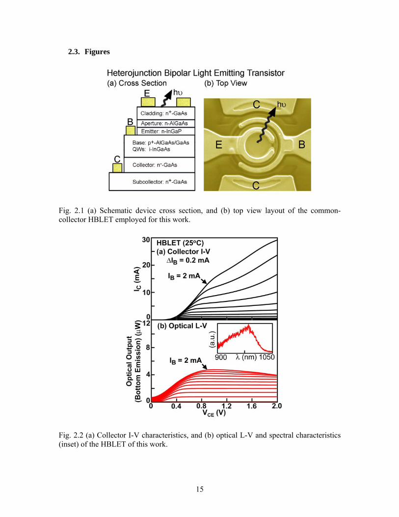
have an oxide aperture diameter, DA, of ~ 6 µm on 10 µm emitter mesas. A schematic of
the device cross section and its top view layout are shown in Fig. 2.1.
The collector I-V and optical output characteristics are shown in Fig. 2.2. The device
exhibits a current gain (= IC/IB) as high as 30 (or 30 dB), e.g., at IB = 2 mA and VCE
= 2 V. The light emission in Fig. 2.2b is measured from the bottom of the device with a
large-area photodetector. A light extraction efficiency of a single escape cone from the
GaAs-air surface, assuming Fresnel reflection losses for normal incidence, is
approximately 1.4%.15 The broad spectral characteristic of the optical output (FWHM =
76 nm) is indicative (the width) of the spontaneous recombination of the HBLET
operation. The HBLET employed here does not incorporate a resonant cavity. For future
work, the use of a resonant cavity could improve optical output extraction to much higher
than that is currently possible in the HBLET of this work. 5
Operating the common-collector HBLET with the BC port as the rf-input allows for
simultaneous electrical-to-optical output conversion, and electrical output gain at the EC
output port. Due to its three-port nature, its optical output can also respond to input
modulation signals at the EC-port, although in this configuration, the device does not
provide a simultaneous electrical output gain at the BC-port. Deploying the EC-port as
the rf-input has the advantage of better matched input impedance (50 standard) for
maximal power transfer. The BC-port input impedance is generally higher than the EC-
input impedance due to the reverse-biased BC junction, and can be advantageous where
high input impedances are desirable for maximizing circuit performances. In the present
8
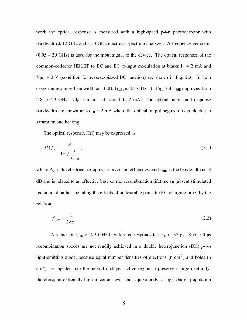
work the optical response is measured with a high-speed p-i-n photodetector with
bandwidth ≥ 12 GHz and a 50-GHz electrical spectrum analyzer. A frequency generator
(0.05 – 20 GHz) is used for the input signal to the device. The optical responses of the
common-collector HBLET to BC and EC rf-input modulation at biases IB = 2 mA and
VBC ~ 0 V (condition for reverse-biased BC junction) are shown in Fig. 2.3. In both
cases the response bandwidth at -3 dB, f3 dB, is 4.3 GHz. In Fig. 2.4, f3dB improves from
2.8 to 4.3 GHz as IB is increased from 1 to 2 mA. The optical output and response
bandwidth are shown up to IB = 2 mA where the optical output begins to degrade due to
saturation and heating.
The optical response, H(f) may be expressed as
0
3
( ) ,1
dB
AH f
fj
f
(2.1)
where Ao is the electrical-to-optical conversion efficiency, and f3dB is the bandwidth at -3
dB and is related to an effective base carrier recombination lifetime B (absent stimulated
recombination but including the effects of undesirable parasitic RC-charging time) by the
relation
3
1
2dBB
f (2.2)
A value for f3 dB of 4.3 GHz therefore corresponds to a B of 37 ps. Sub-100 ps
recombination speeds are not readily achieved in a double heterojunction (DH) p-i-n
light-emitting diode, because equal number densities of electrons (n cm-3) and holes (p
cm-3) are injected into the neutral undoped active region to preserve charge neutrality;
therefore, an extremely high injection level and, equivalently, a high charge population

9
(since Iinject/q = Brad·n·p·Vol = n·Vol/B ) are required in order to achieve high
recombination speeds. In a HBLET, the holes are built-in by p-doping in the base, and
re-supplied by an ohmic base current, while the (minority carrier) electrons are injected
from the heterojunction emitter. Moreover, as opposed to the charge “pile-up” condition
in a double heterojunction p-i-n diode, the dynamic “tilted” charge flow condition is
maintained in the base of the transistor with the electrical collector (reverse-biased BC
junction) in competition with base recombination. Because of the “tilted” base
population, current flow is a function of the slope of the charge distribution, thus making
possible high current densities without requiring extreme carrier densities. The
heterojunction bipolar transistor (HBT) n-p-n structure, therefore, possesses intrinsic
advantages (in how charge is handled) over the double heterojunction p-i-n structure.
Because of the transistor action, i.e., the electrical collector junction collecting charge in
reverse-bias in conjunction with the base quantum-well acting as an optical collector,
collecting charge for radiative recombination, the injected minority carriers that do not
recombine within the transit time from emitter to collector are “discharged” (removed)
from the base region. Due to the thin base (WB = 1358 Å), the intrinsic emitter-to-
collector transit time given by the relation t = WB2/2D (D ≈ 26 cm2/s) is estimated to be
3.6 ps. The intrinsic recombination speed in the base of the transistor must therefore be
of the same order of magnitude as the transit time.16 Therefore, the 37 ps lifetime
demonstrated in our work can still be improved towards its intrinsic speed.
Concluding, the 37 ps carrier lifetime observed in the HBLET of this work
indicates that spontaneous recombination can be “fast,” and higher modulation speeds are
possible by further reducing the undesirable parasitics. In addition, due to the lesser

10
signal attenuation slope of -20 dB per decade beyond the 3 dB bandwidth in contrast to
the -40 dB per decade slope of laser response, an HBLET could potentially be deployed
at data rates much higher than 4.3 Gb/s. Together with the advantages of higher yield,
reduced complexity, and three-terminal high-speed modulation capabilities as both a
transistor (amplifier and switch) and electrical-to-optical converter, the HBLET could be
an attractive solution for short range optical data communications. Its fast spontaneous
recombination lifetime is advantageous for development of high-speed semiconductor
lasers and for integrated optoelectronics.
2.2. Lateral Scaling Toward GHz Operation
In this work, the devices are fabricated employing standard etching and contact
metallization steps, and the emitter aperture widths of 5 µm, 8 µm, and 13 µm are
achieved by lateral oxidation of the n-Al0.98Ga0.02As layer.
The collector I-V characteristics for HBLETs with aperture widths of 5 and 13 µm and
a tilted top view SEM micrograph of the HBLET are shown in Fig. 2.5. Figure 2.6 shows
the corresponding optical light output characteristic L-IB as measured from the bottom-
side of the devices. At comparable base currents IB, the device with a 5 m aperture
achieves 2.4 times higher current gain than the 13 m device. The 13 m HBLET,
however, produces an optical output 2.4 times higher. The current gain, and optical
output saturate at high bias conditions (VCE ≥ 2 V) due to excessive heating as the
devices are on semi-insulating substrate and operated without any temperature control.
While total recombination radiation increases for the larger device, only a fraction of the
radiative recombination occurs within the intrinsic transistor base region. Due to the
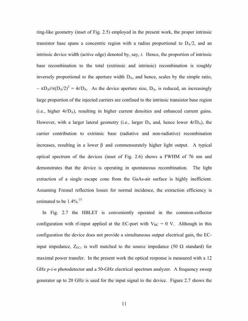
11
ring-like geometry (inset of Fig. 2.5) employed in the present work, the proper intrinsic
transistor base spans a concentric region with a radius proportional to DA/2, and an
intrinsic device width (active edge) denoted by, say, t. Hence, the proportion of intrinsic
base recombination to the total (extrinsic and intrinsic) recombination is roughly
inversely proportional to the aperture width DA, and hence, scales by the simple ratio,
~ DAt/(DA/2)2 = 4t/DA. As the device aperture size, DA, is reduced, an increasingly
large proportion of the injected carriers are confined to the intrinsic transistor base region
(i.e., higher 4t/DA), resulting in higher current densities and enhanced current gains.
However, with a larger lateral geometry (i.e., larger DA and, hence lower 4t/DA), the
carrier contribution to extrinsic base (radiative and non-radiative) recombination
increases, resulting in a lower and commensurately higher light output. A typical
optical spectrum of the devices (inset of Fig. 2.6) shows a FWHM of 76 nm and
demonstrates that the device is operating in spontaneous recombination. The light
extraction of a single escape cone from the GaAs-air surface is highly inefficient.
Assuming Fresnel reflection losses for normal incidence, the extraction efficiency is
estimated to be 1.4%.15
In Fig. 2.7 the HBLET is conveniently operated in the common-collector
configuration with rf-input applied at the EC-port with VBC = 0 V. Although in this
configuration the device does not provide a simultaneous output electrical gain, the EC-
input impedance, ZEC, is well matched to the source impedance (50 standard) for
maximal power transfer. In the present work the optical response is measured with a 12
GHz p-i-n photodetector and a 50-GHz electrical spectrum analyzer. A frequency sweep
generator up to 20 GHz is used for the input signal to the device. Figure 2.7 shows the

12
maximum bandwidth optical response of 4.3, 2.8, and 1.8 GHz achieved by HBLETs of
aperture size DA = 5, 8, and 13 µm, respectively. Higher bandwidths are attained with
HBLETs employing a smaller aperture because a larger proportion of radiative
recombination is confined to the intrinsic base of the HBLET where the intrinsic
recombination speed of the carriers is faster, consistent with the observations derived
from the collector I-V characteristics (Fig. 2.5) and optical L-IB (Fig. 2.6). The plot of
the optical bandwidth vs. the bias base current IB for HBLETs of various aperture sizes
(Fig. 2.8) shows the increase in the optical bandwidth as the bias current (IB and hence, IE)
is increased. The maximum bandwidth is achieved where the optical and electrical
characteristics begin to saturate due to heating, as is evident from Figs. 2.5 and 2.6.
In the absence of stimulated recombination, we can simply express the optical
response as a single-pole transfer function H(f) with f-3dB representing the -3 dB
frequency. The value f-3dB is related to an extrinsic base carrier recombination lifetime B
by f-3dB = 1/(2B). Therefore, an extrinsic B of 37 ps is inferred from the value f-3dB =
4.3 GHz (DA = 5 m), while a B of 88 ps is obtained for a 13-m-aperture device.
Lateral extrinsic recombination therefore forms an equivalent parasitic-like RC-charging
time that limits the optical bandwidth of the device. Therefore, by lateral scaling, we can
improve the device’s performance by “channeling” (via high current densities) and
“limiting” (via smaller apertures) the carriers to feed only radiative recombination
originating or emanating from the intrinsic transistor base. Due to the presence of a finite
(parasitic) lateral edge in the device construction, the B obtained of 37 ps is still
dominated or limited extrinsically. This shows that the intrinsic transistor base

13
recombination lifetime can be much faster than 37 ps, and implies that an even higher
spontaneous optical bandwidth is possible.
To compare the performance of light emitters of LEDs6, 17, 18 and LETs of this work,
the optical bandwidth and the corresponding recombination lifetime are plotted as a
function of the average volume current density, J/d (A cm-3), in Fig. 2.9. J is the average
recombination current density defined as J = IB/(DA2/4) and d is the thickness of the
active region (i.e., the base region for an LET, and the active layer for a double
heterostructure LED). The bimolecular recombination lifetime and the optical bandwidth
of heavily doped double heterostructure LEDs under low level injection are generally
found to be consistent with those predicted by the relation, B = 1/(Brad·NA), where Brad ~
1.4 x 10⁻¹⁰ cm3/s is the bimolecular recombination constant. A double heterojunction
LED does not readily demonstrate sub-100 ps recombination speeds because it is a
“charge pile-up” device, and hence extreme doping and (injected) minority carrier
densities are required to achieve high recombination rates (and modulation speeds).
Moreover, a heavily-doped active region (NA ~ 1020 cm-3) results in low internal quantum
efficiency due to impurity and defect recombination.
Concluding, we have demonstrated the lateral scaling of the heterojunction bipolar
light-emitting transistor to improve both its electrical and optical characteristics. The fast
recombination dynamics of the intrinsic transistor can be harnessed by scaling down the
emitter aperture from 13 to 5 µm to reduce lateral extrinsic parasitic-like RC charging.
We have thus shown that an overall extrinsic recombination lifetime of 37 ps (f3dB = 4.3
GHz) can be achieved. Even higher bandwidths are possible by the further reduction of
undesirable parasitic regions and charging time. The fast spontaneous modulation speeds,

14
together with the high yield and reliability due to ease of fabrication and threshold-less
operation of the LET, offers an attractive alternative to laser sources, especially for use in
short range optical data communications and interconnections.
15
2.3. Figures
Fig. 2.1 (a) Schematic device cross section, and (b) top view layout of the common-collector HBLET employed for this work.
Fig. 2.2 (a) Collector I-V characteristics, and (b) optical L-V and spectral characteristics (inset) of the HBLET of this work.

16
Fig. 2.3 Optical response of the common-collector HBLET to (a) EC rf-input, and (b) BC rf-input.
Fig. 2.4 The 3 dB bandwidth f3 dB as recombination base current IB is increased while maintaining VBC = 0 V, and (inset) typical optical output L-IB characteristic as measured from the device bottom.

17
Fig. 2.5 HBLET collector I-V characteristics corresponding to emitter aperture sizes (a) DA=5 m and (b) DA=13 m, and the scanning electron micrograph (SEM) of a DA= 5 m HBLET (inset).
Fig. 2.6 HBLET optical light output L-IB characteristics (device of Fig. 2.5) for VBC = 0 V as measured from the bottom, and the optical spectrum (inset).

18
Fig. 2.7 The maximum optical response achieved by common-collector HBLETs with emitter aperture sizes DA = 5, 8, and 13 m.
Fig. 2.8 The dependence of HBLET optical bandwidth on aperture size and bias base current IB for VBC = 0 V.
19
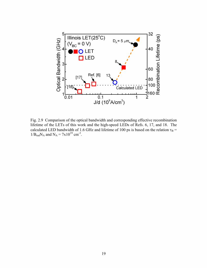
Fig. 2.9 Comparison of the optical bandwidth and corresponding effective recombination lifetime of the LETs of this work and the high-speed LEDs of Refs. 6, 17, and 18. The calculated LED bandwidth of 1.6 GHz and lifetime of 100 ps is based on the relation B = 1/BradNA and NA = 7x1019 cm-3.

20
3. DESIGN OF MULTI-GHZ TILTED-CHARGE LIGHT-EMITTING DIODES
3.1. Theory and Characterization of Tilted-Charge LED
In the present work, we show how the action of the collector in a transistor may be
extended and incorporated into the design of a carrier drain in light-emitting diodes
(LEDs) to enable GHz bandwidth operation. We demonstrate a different form of light-
emitting diode, an asymmetrical two-junction tilted-charge LED, utilizing an n-type
“drain” layer beneath the p-type “base” quantum-well (carrier and photon) active region
capable of modulation at a -3 dB bandwidth up to 7 GHz and an effective B of 23 ps.
In an n-p-n (and similarly p-n-p) transistor, the electrical base-collector (BC) junction
in reverse bias establishes a zero base population density at the boundary of the base and
the collector. Because minority carriers are injected and transported from the emitter (E),
the boundary condition at the collector-“drain” end results in a tilted base charge
population with charge flow of carriers from top to bottom of the QW base active region
(Fig. 3.1). This follows from current continuity. The injected minority carriers that
recombine in the base form the base current, IB, while carriers that are too “slow” to
recombine within the transit time from the emitter to the collector-“drain”, t, are
removed by the base to drain junction reverse bias field (the “drain” current, ID, Fig. 3.1).
Therefore, the charge population in the base of the transistor can be modulated at intrinsic
(parasitic-free) speeds corresponding to an effective recombination lifetime B ~ t.
Assuming a tilted triangular population, we approximate t as WB2/2D where WB (Fig. 3.1)
is the base width, or emitter-to-“drain” distance, and D is the diffusion constant. For a
thin-base transistor where WB ~ 1000 Å, t is typically on the order of several
picoseconds. Taking into account the presence of parasitics due to finite non-zero

21
junction capacitances and ohmic losses, we expect B in the sub-100 ps range. The
possibility of “fast” picosecond recombination dynamics (induced with a tilted-charge
base population) provides the basis for gigahertz modulation of the light-emitting
transistor, and now, in the present work, the light-emitting diode.
The epitaxial layers of the crystal used for the asymmetric two-junction tilted-charge
light-emitting diode consist, upward from the substrate, a 3000 Å n-type doped GaAs
buffer layer, a 500 Å graded Al0.30Ga0.70As confining layer, a 213 Å graded
Al0.30Ga0.70As to Al0.90Ga0.10As oxide buffer layer, a 595 Å n-type Al0.98Ga0.02As
oxidizable aperture layer and another 213 Å graded Al0.90Ga0.10As to Al0.30Ga0.70As oxide
buffer layer. A 557 Å n-type GaAs contact layer, a 120 Å InGaP etch stop layer, and a
2871 Å undoped “drain” layer are grown on top. The “drain” layer is just beneath the
1358 Å base layer, which includes two undoped 112 Å InGaAs quantum wells and an
Al0.05Ga0.95As layer with average doping of 3x1019 cm-3. The heterostructure emitter
consists of a 511 Å n-type In0.49Ga0.51P layer, a 213 Å graded Al0.30Ga0.70As to
Al0.90Ga0.10As oxide buffer layer, a 595 Å n-type Al0.98Ga0.02As oxidizable aperture layer,
another 213 Å graded Al0.90Ga0.10As to Al0.30Ga0.70As oxide buffer layer, and a 500 Å
graded Al0.30Ga0.70As confining layer. The structure is completed with a 2000 Å GaAs
top contact layer.
The asymmetric two-junction tilted-charge LED is fabricated by first performing wet
etching steps to form emitter and base-“drain” mesas, followed by an isolation etch from
the sub-“drain” layer to the substrate. Metallization steps are then performed to provide
the required electrical contacts. For this work we do not employ any optical coatings. A
diagram of the device in cross section is shown in Fig. 3.1. The completed LED has only

22
two terminals: (a) a contact to the emitter layer, and (b) another across the base and
“drain” layers. The base-“drain” forms a p-n junction with a reverse built-in field that is
maintained by a common potential (zero potential difference) obtained via a common
contact metallization extending to the base (Fig. 3.1). The zero base-“drain” potential
difference ensures that there is no base charge population density at the base-“drain”
boundary, hence establishing a dynamic “tilted” emitter-to-“drain” population in the
base.16 The “drain” layer performs therefore a role similar to the collector in a three-
terminal HBLET. It allows excess minority carriers to be removed from the base (ID),
“swept” from base to “drain” by the built-in field at the base-“drain” p-n junction. Base
carriers in transit from the emitter to the “drain” that do not recombine within the base
transit time are removed, or “drained.” This enables fast modulation of the tilted-charge
LED by preventing the build-up of “slow” charge in the base. The tilted-charge LED
possesses the high-speed optical modulation characteristics of an HBLET.
The tilted-charge LED can be biased as a usual two-terminal device, simply operating
faster. Externally the tilted-charge LED displays an electrical I-V characteristic
resembling that of a p-n junction diode (Fig. 3.2). The “turn-on” voltage is determined
by the emitter-base potential difference since the base and “drain” are metalized and
unified in potential. A scanning electron micrograph (top-view) of the completed tilted-
charge LED is shown in the inset of Fig. 3.2. The L-IE optical output characteristic
shown in Fig. 3.3 is obtained from the bottom emission (through the substrate) of the
device. The broad radiative emission spectrum (FWHM ~ 96 nm) of the inset shows that
the LED is operating in spontaneous recombination. The spectral peak occurs at =
1000 nm, corresponding to the ground state transition (1.24 eV) of the InGaAs quantum-
23
wells. The optical output saturates with IE beyond 10 mA as the internal “transistor” gain,
= ID/IB, increases resulting in the base (recombination) current, IB = IE / (+1)
saturating. The measured optical output efficiency of the C-doped tilted-charge LED can
be obtained readily from Fig. 3.3. The optical output is in the low microwatt range
because the light extraction efficiency, assuming a single escape cone from the
semiconductor GaAs-air interface, is only about 1.4%.15 The measured efficiency
decreases from 1.03 W/mA at the peak of the light output (IE = 20 mA) to 0.23 W/mA
at 60 mA; however, the -3 dB bandwidth improves significantly from 1.2 to 7 GHz (Fig.
3.4). Considering the low light extraction efficiency of 1.4%, the “internal” optical
efficiency is, actually, much higher. These diodes in future work can obviously be
improved with reflecting coatings or by incorporating resonant cavities in the
heterostructure crystal.5 Compared to the conventional C-doped LED with efficiency of
0.4 W/mA and bandwidth of 1 GHz,17 the tilted-charge LED maintains a reasonable
efficiency but has a considerably higher modulation speed owing to its capability to
remove slowly-recombining excess carriers from the active region, allowing only “fast”
recombination as a consequence of a drain layer beneath the quantum-well active layer.
In the present work, the optical output is obtained conveniently from the device top with
a fiber, and is measured with a 12 GHz p-i-n photodetector connected to an Agilent
N5230A network analyzer. The optical response of the tilted-charge LED for IE = 40, 50,
and 60 mA is shown in Fig. 3.4. The data show an excellent fit to a single-pole response
of the form, H(f) = Ao/(1+jf/f3 dB) where f3 dB = 1/(2B). We obtain a -3 dB bandwidth,
f-3dB, of 7 GHz at IE = 60 mA, corresponding to an effective B = 23 ps.

24
Concluding, we have fabricated and demonstrated a different form of light-emitting
diode, the tilted-charge LED, which is capable of multi-GHz modulation bandwidth. We
show that the idea and role of a collector in a light-emitting transistor or triode can be
adapted in the form of a “drain” layer in an LED to improve its speed. The tilted-charge
LED, a two-terminal device, has, for some purposes, the advantage of using less crystal
area, is simpler to fabricate at high yield, and is easy to package and use. The potential of
multi-Gigabit spontaneous operation at low current level (no laser threshold) makes the
tilted-charge LED attractive for use in short range optical data communication.
3.2. 4 GHz 2x2 Integrated LED Array
In the present work, we show that the tilted-charge LED can be operated in an array
configuration without loss of speed and at much higher (multi-fold) output level.
To achieve maximum optical output power, the effective optical active (light-emitting)
area can be increased by operating many LEDs in parallel as an integrated array. A
parallel array structure is a simple solution to overcome current crowding as the optically
active area is increased19 without loss of speed of an individual element, a single diode.
The fabrication process of a tilted-charge LED consists of first performing the wet
etching steps to form the emitter and base-drain mesas, followed by an isolation etch
down to the semi-insulating substrate. The emitter and base-drain contacts are then
deposited by standard lithography and metallization. Finally planarization, a via hole
etch, and pad metallization are performed to complete the fabrication process. No optical
coating and resonant cavity are employed in this work. The schematic of the completed

25
device cross section is shown in Fig. 3.5, which also shows the main device layers and
the base-drain internal shorting.
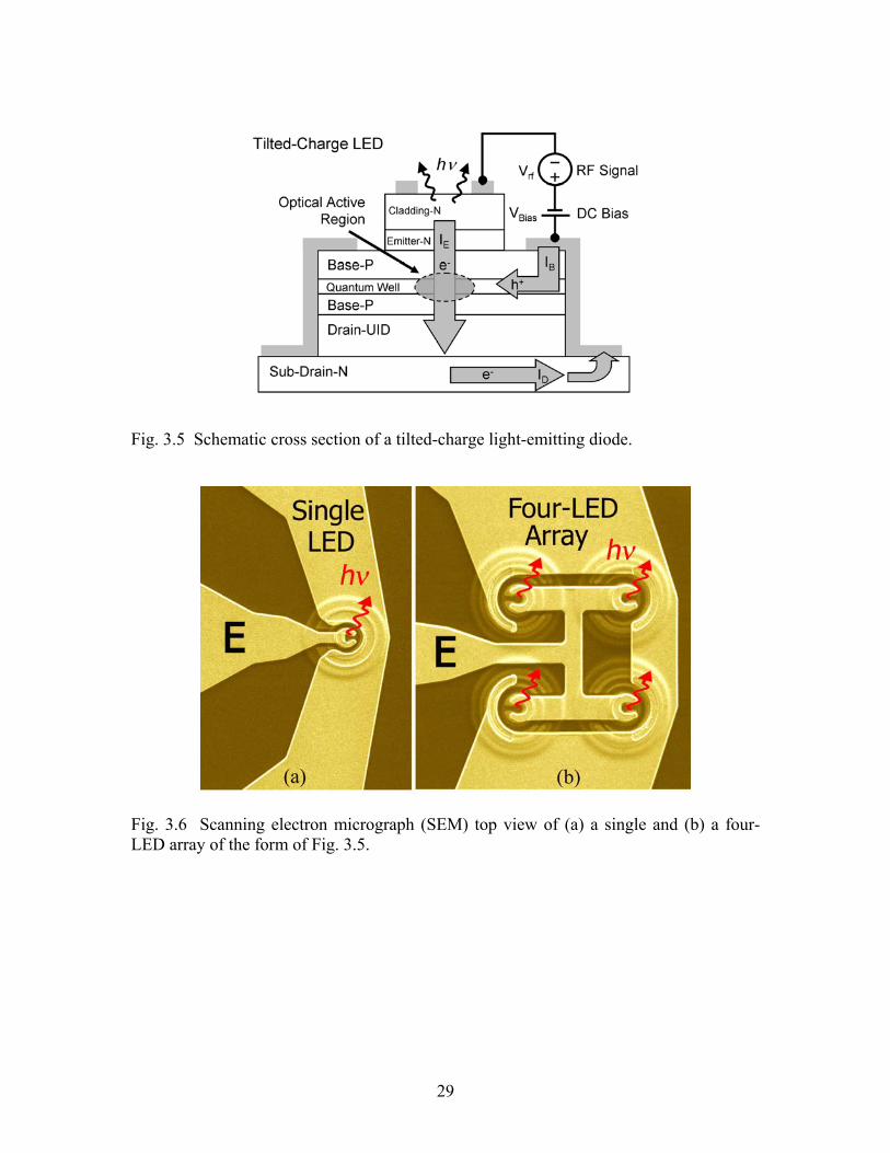
Scanning electron micrographs (top view) of a tilted-charge single and a four-LED
array are shown in Fig. 3.6. The emitter mesa diameter of the single LED is 10 m,
while the four-LED array consists four separate (electrically-isolated) single LEDs biased
by a common electrical input, IE. The distance between two adjacent LEDs is 30 m.
The purpose of the array design is to be able to combine the optical power with no loss of
the modulation bandwidth of a single element, which is determined by the separate
emitter top geometry, not the array common bottom geometry.
Figure 3.7 shows the optical power output (L) measured from the bottom of the
devices with a large area detector versus bias current (IE) for (a) a single LED and for (b)
a four-LED array. The maximum optical output of the four-LED array and its
corresponding bias current is about 3.3 times higher than that of the single LED. The
current distribution is not fully uniform (3.3x signal vs. 4x) because of heating, especially
at higher bias currents. Assuming a single escape cone from the semiconductor GaAs-air
interface, we estimate a light extraction efficiency of 1.4%.15 Hence, the total light
output of the LED is estimated to be 2.3 mW. As IE is increased beyond 10 mA for the
single LED, the optical output starts to saturate as a consequence of the increasing
internal transistor gain, = ID/IB, which results in the base (recombination) current, IB =
IE / (+1), remaining unchanged. The same observation applies to the array but at higher
saturation current.
Figure 3.8 shows the electrical I-V characteristics of the tilted-charge LED. Because
the base and drain layers are now held at equal potential, the turn-on voltage is the
26
emitter-base potential difference. The four-LED array has a lower “turn-on” voltage and
lower resistance due to parallel operation of the multiple LEDs. The measured
resistances of (a) the single and (b) the array LEDs at the point where the optical output
starts to saturate are: (a) 6.7 (IE = 30 mA) and (b) 2.8 (IE = 100 mA), respectively.
The lower input impedance as a function of frequency is shown in the inset of Fig. 3.8,
where the DC bias current IE is 100 mA for the four-LED array, and 30 mA for the single
LED. The input impedance of the four-LED array is one third that of the single LED,
which is poorer impedance-match (to 50 for rf modulation.
The optical response of the device is obtained from the aperture top emission via fiber
coupling to a 12 GHz p-i-n photodetector. The optical response of the tilted-charge
single and four-LED array, and the corresponding curves fitted to a single-pole response,
are shown in Fig. 3.9. The data show an excellent fit to the form, H(f) = Ao/(1+jf/f3 dB).
Both the single LED and four-LED array, though less impedance-matched, show a -3 dB
bandwidth, f-3dB, of 4.3 GHz at similar IE current density. The 4.3 GHz modulation
bandwidth of the four-LED array indicates that the array design indeed provides higher
optical output with no loss in the modulation bandwidth.
Concluding, we have successfully integrated four tilted-charge LEDs into an array,
and demonstrated more than a three times increase in the combined total optical output.
The LED array can be modulated with a -3 dB bandwidth of 4.3 GHz, thus maintaining
the highest performance of the individual components. At the expense only of occupying
more chip space, an LED array offers a simple viable solution to increasing the intensity
of the device optical output while preserving the high-speed performance of the
individual components.

27
3.3. Figures
Fig. 3.1 Cross section (diagram) of a tilted-charge light-emitting diode (LED) with a p-type “base” quantum-well active region.
Fig. 3.2 The I-V characteristic of the tilted-charge LED (Fig. 3.1) and a device SEM picture (inset).

28
Fig. 3.3 Tilted-charge LED optical light output L-I characteristic measured from the device (Fig. 3.2) substrate bottom, and the output optical spectrum (inset).
Fig. 3.4 The optical output response of the tilted-charge LED (Fig. 3.2) at bias currents IE = 40, 50, and 60 mA showing the -3 dB frequency f3dB of 3.2, 5, and 7 GHz, respectively.
29
Fig. 3.5 Schematic cross section of a tilted-charge light-emitting diode.
Fig. 3.6 Scanning electron micrograph (SEM) top view of (a) a single and (b) a four-LED array of the form of Fig. 3.5.

30
Fig. 3.7 (a) Tilted-charge single and (b) four-LED array optical light output L-I characteristics measured from the device bottom.
Fig. 3.8 The I-V characteristics of (a) tilted-charge single and (b) a four-LED array. The inset shows the device, (a) and (b), input impedance as a function of frequency.

31
Fig. 3.9 The optical response of (a) the single LED of Fig. 3.5 biased at IE = 30 mA, and (b) the four-LED array biased at IE = 100 mA. The -3 dB frequency response of both is f3dB = 4.3 GHz.

32
4. MICROCAVITY QUANTUM-WELL VERTICAL CAVITY SURFACE-
EMITTING LASERS
4.1. Microwave Characterization of Purcell Enhancement
Microcavity light-emitting devices are of interest in the pursuit of threshold-free light-
emitting diodes (LEDs or lasers) for optical communications at high modulation speeds.
Purcell proposed (1946) that the upper-state, lower-state spontaneous transition rate of a
“light”-emitting system could be enhanced (here electron-hole [e-h] spontaneous
recombination rate) in a small volume microcavity with a high Q.20 The spontaneous e-h
recombination lifetime reduction is usually observed by time-resolved (optical input-
output) photoluminescence (PL) or phase-resolved spectroscopy experiments, with
auxiliary spectral emission data revealing the reduction in optical modes and the narrower
emission bandwidth of the cavity modes.21-24 This has been reported for various
photopumped semiconductor systems employing quantum-dots (QDs)21, 22 and micro-
disks.23, 24 In the present work we describe a more powerful microwave method,
electrical input and optical output, a distinct advantage in signal separation, to probe
directly and analyze in detail the microcavity resonance effects of a QW vertical cavity
surface-emitting laser (VCSEL). We measure a Purcell enhancement factor of 2.08 times,
in agreement with earlier more limited spectral emission data.
The devices employed in the present study are p-i-n diode VCSELs. The bottom
mirror consists of 34 periods of n-doped Al0.12Ga0.88As/Al0.9Ga0.1As Bragg reflectors
(DBR), followed by the active region consisting of three GaAs quantum wells embedded
in an undoped Al0.3Ga0.7As separate confinement heterostructure (SCH) layer. The now
standard buried optical- and population-defining oxide aperture layer6 consists of 300 Å
Al0.98Ga0.12As, followed by a 22 period DBR of carbon-doped Al0.12Ga0.88As/Al0.9Ga0.1As

33
forming a vertical longitudinal cavity. The microcavity VCSELs are fabricated by first
masking and forming the mesa with inductively coupled plasma dry etching. The oxide
apertures are then formed as usual by wet oxidation25 and accurate calibration and close
monitoring of the oxidation time. Dummy samples are used to calibrate the oxidation
rate and aperture depth before every process. Aperture diameters are determined by
taking scanning-electron micrographs (SEM) of dummy-sample cross-section. Standard
metallization of p-contacts and n-contacts are then performed, followed by wafer
planarization, via-hole etching, and pad metallizations to complete the devices.
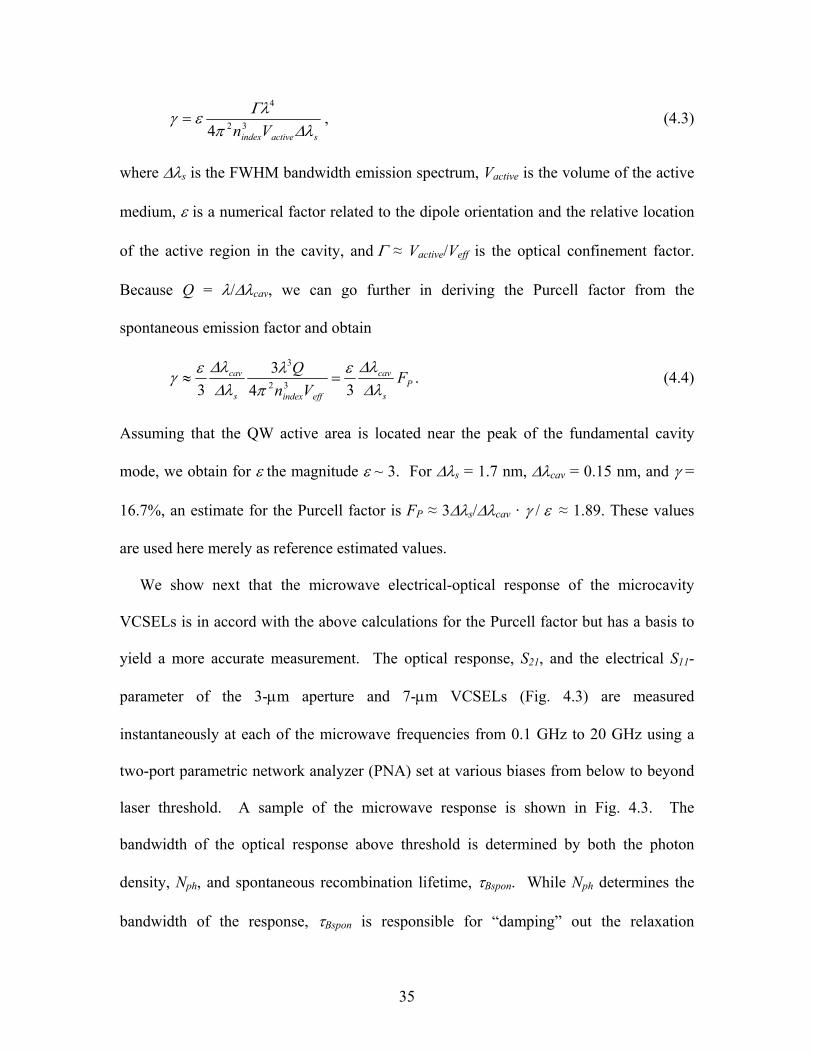
In Fig. 4.1 the emission spectra are shown for VCSELs with two aperture sizes, dA = 7
and 3 m, operating in the sub-threshold (spontaneous) regime. The number of
transverse optical modes is reduced from approximately ten for a 7 m aperture (I = 600
A) to one dominant fundamental mode with two weak higher order side-modes for a
VCSEL with an aperture dA = 3 m operating below threshold at current I = 150 A. The
separation between the optical modes of the lowest and second lowest order of the
VCSELs is 1.45 nm for aperture dA = 3 m, and 0.22 nm for dA = 7 m. By
approximating the VCSEL structure (Fig. 4.1) as a circular waveguide, we can write the
dispersion relation26 as kz2 = 2 – (2mn/do)
2, where kz is the wave vector normal to the
device plane, do is the modal diameter, and mn is the nth root of the mth order Bessel
function. For the two lowest Bessel function roots, 01 = 2.4 and 11 = 3.8, the modal
diameter, do, is estimated as 4.2 m for dA = 3 m, and 10.7 m for dA = 7 m. The
spontaneous spectrum of the 3 m VCSEL at 90 A exhibits an optical mode FWHM
bandwidth cav of 0.15 nm, giving a cavity Q = /cav = 5700. The reduction in the
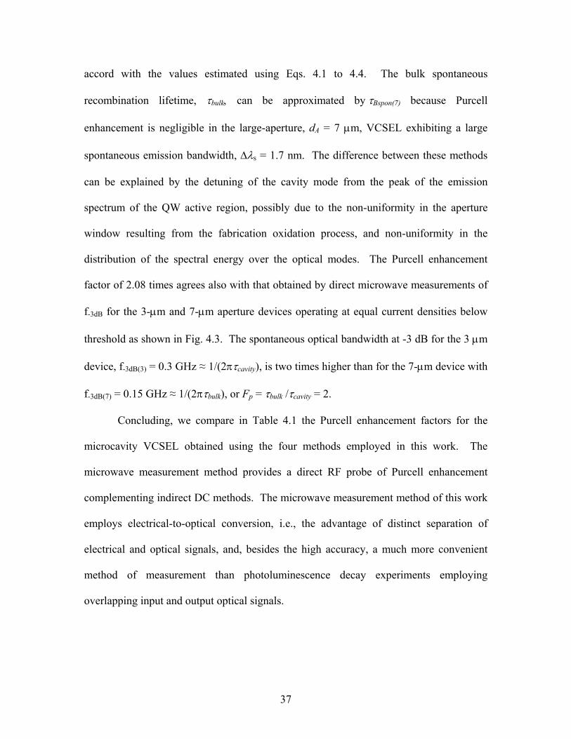
threshold current ITH is consistent with the reduction in device volume as the aperture size

34
is decreased. A plot of ITH vs. aperture area, dA2/4 (Fig. 4.2), yields (consistently) a
threshold current density JTH = 2 kA/cm2, showing that as the aperture size is decreased
the non-radiative recombination remains fixed, and does not affect the effective
spontaneous lifetime.
Spectral emission data allow us to estimate the Purcell enhancement factor FP as20
3
24
3
indexeffcavity
bulkP nV
QF
, (4.1)
where bulk is the bulk spontaneous radiative lifetime, cavity is the cavity-enhanced
spontaneous lifetime, Veff is the effective modal volume, and nindex is the effective index
of refraction. For the 3-m-aperture -thickness cavity VCSEL, Veff = (do/2)2(/nindex),
nindex(AlGaAs) = 3, and the Purcell factor is 2.53.
In addition to the enhancement in the spontaneous lifetime, microcavity resonators
result in enhancement of the spontaneous emission factor, , which provides a measure of
the fraction of the total spontaneous radiative emission power in the fundamental cavity
mode. This offers another approach to estimate the Purcell factor. If we assume that the
spontaneous radiation is uniform across the optical modes, the spontaneous emission
factor can be estimated as one half the inverse of the number of modes in the
spectrum,27, 28
1spectrumemission in modes ofnumber 2
1 . (4.2)
Since there are approximately three modes in the emission spectrum of the 3-m device,
is estimated to be 16.7%. A more elaborate expression for the spontaneous emission
factor is given by28
35
sactiveindexVn
32
4
4 , (4.3)
where s is the FWHM bandwidth emission spectrum, Vactive is the volume of the active
medium, is a numerical factor related to the dipole orientation and the relative location
of the active region in the cavity, and ≈ Vactive/Veff is the optical confinement factor.
Because Q = /cav, we can go further in deriving the Purcell factor from the
spontaneous emission factor and obtain
Ps
cav
effindexs
cav FVn
Q
34
3
3 32
3
. (4.4)
Assuming that the QW active area is located near the peak of the fundamental cavity
mode, we obtain for the magnitude ~ 3. For s = 1.7 nm, cav = 0.15 nm, and =
16.7%, an estimate for the Purcell factor is FP ≈ 3s/cav · ≈ 1.89. These values
are used here merely as reference estimated values.
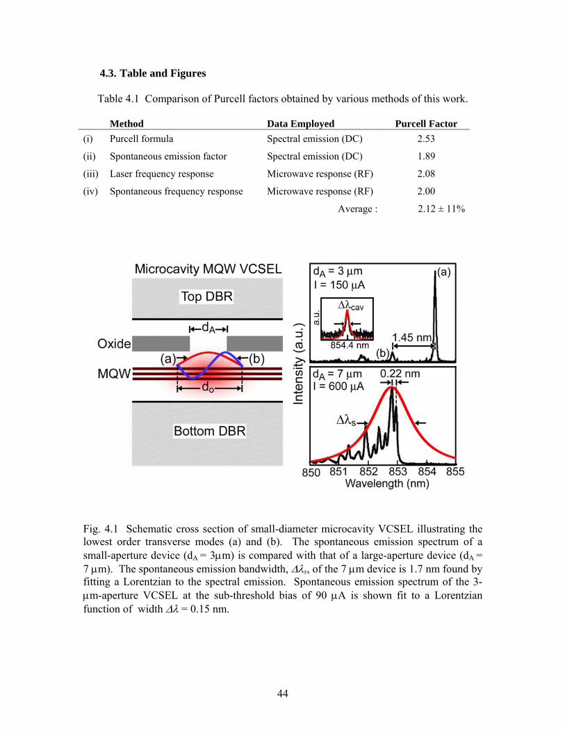
We show next that the microwave electrical-optical response of the microcavity
VCSELs is in accord with the above calculations for the Purcell factor but has a basis to
yield a more accurate measurement. The optical response, S21, and the electrical S11-
parameter of the 3-m aperture and 7-m VCSELs (Fig. 4.3) are measured
instantaneously at each of the microwave frequencies from 0.1 GHz to 20 GHz using a
two-port parametric network analyzer (PNA) set at various biases from below to beyond
laser threshold. A sample of the microwave response is shown in Fig. 4.3. The
bandwidth of the optical response above threshold is determined by both the photon
density, Nph, and spontaneous recombination lifetime, Bspon. While Nph determines the
bandwidth of the response, Bspon is responsible for “damping” out the relaxation

36
oscillations. Therefore, the spontaneous recombination lifetime of the VCSEL in full
laser operation can be obtained by fitting the response to a model based on the coupled
carrier-photon rate equations,29 written as
phBspon
gNN
Idt
dN
, (4.5)
and
Bsponph
phph
ph NNgN
dt
dN
, (4.6)
where N is the population inversion number, is the photon group velocity, and g is the
QW gain. The intrinsic device parameters are determined by first extracting the pad
parasitics (pad resistance, capacitance, and inductance) from two-port microwave
measurements of the electrical SHORT, OPEN and THRU structures fabricated on the
same wafer.30 The parasitics, together with the intrinsic VCSEL model,31 are shown in
Fig. 4.3c. In Fig. 4.3 the 3-m device measured microwave responses of (a) f-3dB = 10.8
GHz at I = 1.0 mA and (b) f-3dB = 7.9 GHz at 0.5 mA are fitted to the model. The
intrinsic parameters that produce an excellent fit to the measured laser optical response
corresponding to the L-I and I-V characteristics of the 3-m VCSEL (Figs. 4.1 and 4.2)
are: ph(3) = 3.7 ps, Bspon(3) = 0.51 ns, = 12%, gTH(3) = 30 per cm, and = 1 x 10⁸ m/s.
For the 7-m VCSEL, the intrinsic parameters are: ph(7) = 6.3 ps, Bspon(7) = 1.06 ns, (7)=
4%, and gTH(7) = 18 per cm. The faster Bspon of the 3-m VCSEL and the larger result
in “damped” resonance peaks of lesser magnitude. The spontaneous emission factors are
also in close agreement with the values obtained from Eq. 4.2. The extracted values of
cavity ~ Bspon(3)and bulkBspon(7) give a Purcell enhancement of 2.08 times, essentially in
37
accord with the values estimated using Eqs. 4.1 to 4.4. The bulk spontaneous
recombination lifetime, bulk can be approximated byBspon(7) because Purcell
enhancement is negligible in the large-aperture, dA = 7 m, VCSEL exhibiting a large
spontaneous emission bandwidth, s = 1.7 nm. The difference between these methods
can be explained by the detuning of the cavity mode from the peak of the emission
spectrum of the QW active region, possibly due to the non-uniformity in the aperture
window resulting from the fabrication oxidation process, and non-uniformity in the
distribution of the spectral energy over the optical modes. The Purcell enhancement
factor of 2.08 times agrees also with that obtained by direct microwave measurements of
f-3dB for the 3-m and 7-m aperture devices operating at equal current densities below
threshold as shown in Fig. 4.3. The spontaneous optical bandwidth at -3 dB for the 3 m
device, f-3dB(3) = 0.3 GHz ≈ 1/(2cavity), is two times higher than for the 7-m device with
f-3dB(7) = 0.15 GHz ≈ 1/(2bulk), or Fp = bulk /cavity = 2.
Concluding, we compare in Table 4.1 the Purcell enhancement factors for the
microcavity VCSEL obtained using the four methods employed in this work. The
microwave measurement method provides a direct RF probe of Purcell enhancement
complementing indirect DC methods. The microwave measurement method of this work
employs electrical-to-optical conversion, i.e., the advantage of distinct separation of
electrical and optical signals, and, besides the high accuracy, a much more convenient
method of measurement than photoluminescence decay experiments employing
overlapping input and output optical signals.

38
4.2. Microwave Determination of Electron-Hole Recombination Dynamics from
Spontaneous to Stimulated Emission
In the present work we study, via sensitive microwave measurements, microcavity
QW vertical cavity surface-emitting lasers (VCSELs) operating strongly coupled into a
small, reduced-spread spectral mode density, into faster recombination yielding a broader
laser bandwidth, and damping the resonant peak. The microwave measurements reveal
unambiguously the transition in recombination lifetimes from spontaneous to stimulated
emission, to cut-off by parasitic elements (junction capacitance, etc.) and ancillary
contact circuitry. We show that higher frequency response in the regime below laser
threshold can be explained by the influence of the faster components of recombination.
The devices employed in the present study are p-i-n diode VCSELs. The bottom
mirror consists of 34 periods of n-doped Al0.12Ga0.88As/Al0.9Ga0.1As Bragg reflector
layers (DBR), followed by the active region with three GaAs quantum wells embedded in
an undoped Al0.3Ga0.7As separate confinement heterostructure (SCH) layer. The oxide
aperture layer25 consists of 300 Å of Al0.98Ga0.02As, followed by a 22-period DBR of
carbon-doped Al0.12Ga0.88As/Al0.9Ga0.1As forming a short vertical longitudinal cavity.
The microcavity VCSELs are fabricated by first masking and forming diode mesas with
inductively coupled plasma dry etching. The oxide apertures are then formed as usual by
wet oxidation25 and careful calibration and monitoring of the oxidation time. Standard
metallization of p-contacts and n-contacts is then performed, followed by wafer
planarization, via-hole etching, and pad metallization to complete the devices.
In Fig. 4.4 the optical emission spectra are shown for VCSELs with aperture size dA =
3 m operating in the sub-threshold (spontaneous) region, stimulated, and above

39
threshold (Ith = 0.18 mA) as a laser. There is a dominant fundamental mode (labeled (a))
with two much weaker higher order side-modes below and above threshold (labeled (b)).
The diode spontaneous recombination spectrum at 0.09 mA exhibits an optical mode
FWHM bandwidth, cav, of 0.15 nm, giving a cavity Q = /cav = 5700. For laser
operation at bias current I > 0.25 mA, the linewidth narrows to an apparent Q > 30,000.
The 3 m microcavity VCSEL operates nearly as a single-mode laser with mode spacing
~ 1.45 nm and with the relative intensity of the 2nd order laser mode 25 dB below the
fundamental mode.
The optical output L vs. I characteristic and the derivative dL/dI vs. I (Fig. 4.5) exhibit
a laser threshold, the “kink” in the L-I characteristic, Ith = 0.18 mA. There are three
distinct regions of operation: (i) I < Ith, spontaneous and amplified spontaneous emissions;
(ii) Ith < I < 0.25 mA, the transition to stimulated emission and laser oscillation; and (iii)
I > 0.25 mA, laser operation at constant dL/dI. The behavior of dL/dI indicates the
differential gain, as well as the transition of device operation mode. The superlinear
characteristic of L-I is due to thermal effect caused by the temperature dependence of
gain spectrum and detuning between gain peak and cavity resonance, which is more
pronounced in the single-mode VCSEL due to smaller aperture and higher series
resistance.
The microwave optical and electrical response of the microcavity VCSEL can be used
to identify and resolve in detail the transition from spontaneous to stimulated emission.
The optical response, S21, and electrical S11-parameters of the VCSEL of Fig. 4.4 are
measured instantaneously at each frequency from 0.1 GHz to 20 GHz using a two-port
parametric network analyzer (PNA) set at various biases from below to beyond laser

40
threshold. The pad parasitics (pad resistance, capacitance, and inductance) then can be
extracted from two-port microwave measurements of the electrical SHORT, OPEN and
THRU structures fabricated on the same wafer.30 The extracted pad capacitance is 0.3 pF
and inductance is 22 pH, while the series and parallel pad resistances are 0.3 and 7 Ω.
The intrinsic VCSEL parameters can therefore be de-embedded together with these
parasitics to form the device small signal model.31 The -3 dB bandwidth of the 850 nm
detector is limited to 12 GHz; hence, the frequency response above 12 GHz is limited by
the additional pole of the detector. The plot of f-3dB vs. J (Fig. 4.6) reveals three regions
of operation corresponding to the L-I characteristic of Fig. 4.5.
The increase in the bandwidth in regions (ii) and (iii) of Fig. 4.6 is a result of
stimulated emission and laser operation. As diode laser operation is approached, the
coherent field becomes self-sustaining, gain is “clamped” to cavity loss, and incremental
injected carriers re-supply both stimulated and spontaneous recombination. At this point
the bandwidth of the optical response is determined by both the photon density, Nph, and
spontaneous recombination lifetime, Bspon.16,32,33 While Nph determines the bandwidth of
the response, the fast recombination component (Bspon = fast) is responsible for “damping
out” the relaxation oscillations, resulting in relatively flat frequency response in region
(iii) of Figs. 4.6 and 4.7.
The diode microwave response below threshold in Fig. 4.7(i) is of particular
interest. In this region the gain in stimulated emission due to the QW active medium is
insufficient to overcome the loss of photons from the cavity. As a result, the coherent
field (stimulated emission) will eventually decay at a rate determined by cavity loss, or
photon lifetime, ph. At low current densities (J << 2 kA/cm2) where gain is negligible,

41
the average spontaneous recombination lifetime is given by 1/(2 f-3dB) = 1 ns or f-3dB =
0.15 GHz. As gain is increased (more current) towards threshold, the coherent field
exists longer before decaying (not yet self-sustaining) and thus assists in enhancing
(reducing) the overall recombination lifetime and increasing the bandwidth (f3 dB). In
other words, the diode response below threshold is a manifestation of both spontaneous
and stimulated emission. The increasing spontaneous bandwidth at lower current
densities (i.e. reducing cavity-enhanced spontaneous lifetime, cavity) can be correlated to
the observed spectral narrowing (i.e. reducing cav) from the Purcell enhancement factor
Fp as20
3
24
3
indexeffcavity
bulkP nV
QF
(4.7)
where bulk is the bulk spontaneous radiative lifetime, Veff is the effective modal volume,
nindex is the effective index of refraction, and Q = /cav. As current is increased, more
coherent photon (Nph) is generated, resulting a narrower cav and larger bandwidth.
To distinguish between diode spontaneous and stimulated-emission response, the
optical output signal is “traced” from 0.1 to 20 GHz. Beyond the “corner” frequency
(f-3dB), the diode stimulated-emission response (orange trace) has a characteristic slope of
-40 dB per decade, or more (~ 60 dB per decade), while the spontaneous-emission
response (blue) has a characteristic slope of -20 dB per decade (Fig. 4.7(i)). The diode
optical signal response at lower frequencies (orange line) exhibits stimulated emission
with the modulation amplitude higher and the slope beyond the corner frequency -40 dB
per decade or steeper. As the response curve is traced to higher frequencies, the
amplitude (lower) shifts (descends) by -20 dB per decade. Spontaneous recombination

42
emission is then the “faster” mode of recombination and can (at higher frequencies)
respond with a larger modulation amplitude (Fig. 4.7(i), I = 0.12 mA [f > 0.5 GHz] and
0.15 mA [f > 1 GHz]). These data show that microwave response measurements can be
employed to distinguish between the various components, slow vs. fast, of carrier
recombination.
Spontaneous recombination lifetime is ordinarily expressed as an average
parameter, analogous to the half-life of nuclear decay; therefore, as half of the
electron-hole population “decays” (recombines) over an average “half-life,” there is a
significant carrier population (although a fraction) that decays much faster than the
average. It is the “faster” recombination carriers that respond to the higher microwave
modulation frequencies. For f > 1 GHz, the carriers that can respond to the microwave
signal (a significant fraction) possess a recombination “lifetime” as short as 1/(2f) = 159
ps. Microwave response measurements reveal in the overall population the faster
components of recombination, particularly in the case of smaller devices of appropriate
geometry and boundary conditions (for example, the cavity geometry and form of input-
output contact geometry or a tilted charge population as in the light-emitting transistor or
transistor laser).
Concluding, we have shown with optical microwave modulation response
measurements of the excess carrier lifetime, av (n/avn1/fast+n-n1)/slow,
fast<slow), on a low mode density microcavity VCSEL, that the slower (slow) and faster
(fast) recombination can be separated, making it possible to distinguish unambiguously
between spontaneous recombination and stimulated emission, including laser operation.
It is clear that the size, geometry, and boundary conditions (optical cavity and current

43
contacts) of a crystal, e.g., typical of a microcavity laser, determine (reduce) the carrier
lifetime (spontaneous or stimulated) and hence determine the optical microwave
modulation response.
44
4.3. Table and Figures
Table 4.1 Comparison of Purcell factors obtained by various methods of this work.
Method Data Employed Purcell Factor
(i) Purcell formula Spectral emission (DC) 2.53
(ii) Spontaneous emission factor Spectral emission (DC) 1.89
(iii) Laser frequency response Microwave response (RF) 2.08
(iv) Spontaneous frequency response Microwave response (RF) 2.00
Average : 2.12 ± 11%
Fig. 4.1 Schematic cross section of small-diameter microcavity VCSEL illustrating the lowest order transverse modes (a) and (b). The spontaneous emission spectrum of a small-aperture device (dA = 3m) is compared with that of a large-aperture device (dA = 7 m). The spontaneous emission bandwidth, s, of the 7 m device is 1.7 nm found by fitting a Lorentzian to the spectral emission. Spontaneous emission spectrum of the 3-m-aperture VCSEL at the sub-threshold bias of 90 A is shown fit to a Lorentzian function of width = 0.15 nm.
45
Fig. 4.2 Laser threshold, ITH, of the VCSELs (of Fig. 4.1) vs. aperture area (A = dA
2/4) for various oxide-defined diameters of dA = 3, 6, 7 and 11 m.
Fig. 4.3 Measured and calculated laser frequency response of the microcavity VCSELs of Figs. 4.1 and 4.2 for device (i) with dA = 3 m at biases (a) I = 1.0 mA (f-3dB = 10.8 GHz) and (b) 0.5 mA (f-3dB = 7.9 GHz), and device (ii) with dA = 7 m at biases (c) I = 4.0 (f-3dB = 9.7 GHz) and (d) 2.0 mA (f-3dB = 5.6 GHz). Also shown are the measured spontaneous optical frequency response (below threshold) f-3dB = 0.3 GHz (dA = 3 m) and 0.15 GHz (dA = 7 m), and (iii) the measured and the model of the electrical S-parameters for the device apertures and biases of (a) to (d) with the pad parasitics in series with the intrinsic laser. The series resistances are Rs(3) = 370 and Rs(7) = 88 .

46
Fig. 4.3 Continued.

47
Fig. 4.4 (i) Schematic cross section of a microcavity VCSEL illustrating the lowest order transverse modes (a) and (b). (ii) Spontaneous emission spectrum (experiment) of fundamental mode (a) and second-order mode (b) below laser threshold, I < Ith = 0.18 mA, for cavity diameter dA = 3 m. Laser spectrum for I > Ith .

48
Fig. 4.5 Output light vs. current (L-I) characteristics of the microcavity VCSEL of Fig. 4.4 and derivative, dL/dI (W/A). The three regions of operation are: (i) I < Ith = 0.18 mA, spontaneous and amplified spontaneous emission; (ii) Ith < I < 0.25 mA, transition to laser operation, and (iii) I > 0.25 mA, laser operation at constant dL/dI.
Fig. 4.6 Measured optical microwave modulation bandwidth at -3 dB, f3dB vs. current density, J = I/A, for the VCSEL of Fig. 4.4. The three regions (i), (ii), (iii) correspond to the L-I curve in Fig. 4.5.

49
Fig. 4.7 Measured optical microwave response of the VCSEL (dA = 3 m) of Figs. 4.4 – 4.6 at current: (i) I = 0.09 - 0.18 mA (I = 0.01 mA), spontaneous and amplified spontaneous recombination; (ii) I = Ith = 0.18 to 0.25 mA (I = 0.01 mA), transition to laser operation; (iii) I = 0.5 - 1 mA (I = 0.5 mA) laser operation.

50
5. THE EFFECT OF MICROCAVITY LASER RECOMBINATION LIFETIME ON MICROWAVE BANDWIDTH AND EYE-DIAGRAM
SIGNAL INTEGRITY
In the present work we focus on the spectral and microwave behavior of the VCSEL
form of microcavity laser. A microcavity provides better confinement of optical fields,
i.e., higher Q, and leads to enhancement of the spontaneous emission rate due to the
Purcell effect. By employing an oxide-confined cavity to modify the dipole-field
coupling and reduce the density of available photon modes, we demonstrate improved
microwave performance (f-3dB) and an eight-fold reduction in recombination lifetime (rec)
owing to carriers occupying primarily a single (fundamental) mode of the microcavity
laser. The device with smaller mode volume exhibits much lower threshold current,
larger mode spacing and side-mode suppression ratio (SMSR), as well as higher
modulation frequency bandwidth and data transmission speed. With single-mode
operation and larger SMSR the threshold current of a microcavity laser is less sensitive to
change in the ambient temperature because of locked single-mode operation. In other
words, “threshold-less” behavior is observed in a higher Q microcavity laser. A
microwave method is used to analyze conveniently the reduction in recombination
lifetime in a microcavity laser, based on constructing an equivalent small-signal model
employing S-parameter measurements. Finally, we compare the quality of data
transmission with the change in eye diagrams for single-mode and multimode lasers. The
single-mode (microcavity) laser, because of reduced lifetimes (enhanced recombination),
exhibits faster and flatter frequency response, thus yielding a “cleaner” eye diagram
compared to multimode operation.

51
5.1 Spectral Mode Spacing and Purcell Effect
A schematic cross section of a completed device is shown in Fig. 5.1. The schematic
diagram Fig. 5.1(ii) indicates the possible optical modes introduced inside the
microcavity: (a) 1st order (fundamental), (b) 2nd order, and (c) 3rd order mode. The oxide
aperture diameter is dA, and d0 is the lateral optical mode dimension.
After careful calibration and aperture oxidation, scanning electron microscope (SEM)
images of three devices with different aperture sizes dA are shown here: D1 (2 μm), D2
(2.5 μm), and D3 (3.5 μm). Figure 5.2 shows the diode laser L-I curves measured from a
top fiber and I-V characteristics of three devices. The threshold currents, ITH, for D1, D2,
and D3 are 0.13, 0.16, and 0.20 mA,respectively. The lowest threshold current (0.13 mA)
is obtained without any specific heat dissipation attempt, e.g., lapping and thinning the
substrate. The threshold current density, JTH, is linearly proportional to the aperture areas
with the diameters ranging from 7 m to 3m; at still smaller diameters, thresholds
increase due to excessive heat generation of the larger device resistance. The oxide-
confined aperture improves the overlap of electrical and optical gain owing to better
confinement of the optical field and the current injection, further defining the lateral
optical mode dimension. Together with the vertical DBR mirror, a microcavity laser is
readily formed without suffering high input impedance and optical scattering loss using a
pillar structure. The merit of the microcavity is in providing a low laser threshold due to
“easier” single-mode operation, and finally threshold-less operation.
By adjusting the cavity volume, we can control the optical mode existing in the
microcavity QW laser by a classical electrodynamics determination. A smaller cavity
allows the electromagnetic wave to exist only in a few modes, say, the fundamental mode

52
and a couple of higher order modes as shown in Fig. 5.1(ii). For an oxide-confined
microcavity VCSEL of aperture size dA > 5 µm the optical mode is approximately
circular, but for smaller aperture size dA < 5 µm the optical mode profile will be
elliptical-like owing to the sensitivity of the oxidation procedure and crystal anisotropy.
Ideally, from spectral data on different modes, we can extract the lateral modal profile by
solving the Helmholtz equation numerically under given boundary condition. For a
rough estimate we assume the optical field is confined laterally inside the mode boundary,
and approximate the optical mode profile as rectangular with width a and length b. Since
the carrier distribution and optical lateral dimension profile will change at different bias
current levels, it is necessary to calculate a, b, and L for each bias current. By solving the
Helmholtz equation
2 22 2 202 2
( ) ( , ) ( ) ( , ) 0zE x y k n k E x yx y
, (5.1)
we obtain the Eigen-mode solution satisfying the expression for both the transverse
electrical and transverse magnetic field,
2 222 20 2 2
1.z
m nk k
c n a b
(5.2)
Here kz = l(/L), and m, n, l are positive integers. The quantity k0(m, n) is the propagation
constant in vacuum, L is the upper and lower Bragg reflector spacing in the vertical
direction, and 3.3~ n is the effective refractive index inside the aperture.
Figure 5.3 shows the spectral data for the D1 microcavity laser (ITH = 0.13 mA) at
different bias currents. The 1st (fundamental) mode is labeled as (a), and the 2nd order
mode (b) is 2.45 nm shorter with 32.5 dB suppression at bias current I = 0.8 mA. The
still higher order mode intensity is too weak to be observed. We denote the wavelength

53
of each optical mode as follows, 1st (fundamental) mode at λ(1,1), 2nd order modes at
λ(1,2) and λ(2,1), and 3rd order modes at λ(2,2), λ(1,3) and λ(3,1). From spectral data we
estimate the mode dimensions a, b, and L using Eqs. (5.3) to (5.5) as
2 2 22 20 0 2 2
2 2 3(2,1) (1,1) ,
(2,1) (1,1)k k
n a
(5.3)
2 2 22 20 0 2 2
2 2 3(1,2) (1,1) ,
(1, 2) (1,1)k k
n b
(5.4)
2 2 2
2 2.
2
(1,1)
z
Lk n
a b
(5.5)
In Table 5.1 we summarize the calculated mode dimensions a, b, and L for three
different aperture sizes at bias current I = 0.8 mA. The data show the cavity vertical
distance L is more than 10 times smaller than the lateral dimension a and b; hence, the
fundamental mode wavelength is mainly determined by L as (1,1) nL . The mode
dimensions a and b determine the mode spacing between the fundamental mode and
the 2nd order modes. As shown in Table 5.1, oxide-aperture size reduction decreases the
lateral mode dimensions and enlarges the mode spacing. This shows that optical mode
control can be achieved by “tuning” the oxide aperture size as well as by the vertical
cavity length.
In order to achieve lower threshold current VCSELs, we design the position of the
maximum gain profile aligned with the fundamental cavity modes. For devices with
larger mode spacing, there are fewer modes within the gain profile; i.e., the
fundamental mode will contribute mainly to the increase in optical intensity (photon
density). Carrier re-adjustment in the mode acts as a positive feedback mechanism

54
“tuning” stimulated emission and providing more photon generation in the fundamental
mode. With larger mode spacing, the carrier injection is more “efficiently” concentrated
in only one mode. This behavior can be observed from the spectral data in Fig. 5.3. The
“fast” increase in the fundamental mode results in a larger side-mode suppression ratio
(SMSR) between the fundamental (1st) and the higher order (2nd, 3rd …) cavity modes.
These data explain also why a device with larger mode spacing will have a lower
threshold current and steeper SMSR slope below saturation as shown in Fig. 5.4.
Figure 5.4 shows the SMSR between the fundamental mode and 2nd order modes as a
function of bias current for three devices. The SMSR can be clearly separated into three
regions. For region (I) at bias current I < 0.25 mA, the SMSR increases linearly with
current, indicating that the photon density increases superlinearly with bias current. In
this region the quality factor Q of the fundamental mode (Q = λ/Δλcav) quickly increases
from around 5500 to above 30000 as the bias current increases and the lateral modal
dimension (a, b) decreases. The data show that for the smallest mode-volume device (D1)
most of the injected carriers will be concentrated in the fundamental mode, thus giving a
steeper slope. Generally the smaller the aperture, the steeper the SMSR will increase for
given bias current increase. For region (II) bias current at 0.25 < I < 0.4 mA, the SMSR
reaches its maximum value of ~ 36 dB for D1 (Δλ = 2.45 nm); ~27.5 dB for D2 (Δλ = 1.6
nm); and ~19 dB for D3 (Δλ = 1.0 nm). In this region higher-order modes start to
contribute to the intensity due to saturation of the ground state quantum-well gain profile.
Succeeding carriers (higher level) will then start to participate both in the ground and 1st
excited state transitions, resulting in saturation of the SMSR. For region (III) bias current
at I > 0.4 mA, the differential gain of the fundamental mode is lower than on the 2nd order
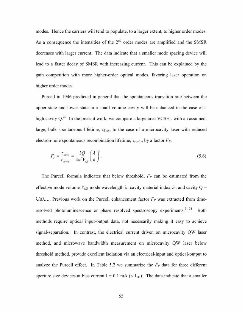
55
modes. Hence the carriers will tend to populate, to a larger extent, to higher order modes.
As a consequence the intensities of the 2nd order modes are amplified and the SMSR
decreases with larger current. The data indicate that a smaller mode spacing device will
lead to a faster decay of SMSR with increasing current. This can be explained by the
gain competition with more higher-order optical modes, favoring laser operation on
higher order modes.
Purcell in 1946 predicted in general that the spontaneous transition rate between the
upper state and lower state in a small volume cavity will be enhanced in the case of a
high cavity Q.20 In the present work, we compare a large area VCSEL with an assumed,
large, bulk spontaneous lifetime, τBulk, to the case of a microcavity laser with reduced
electron-hole spontaneous recombination lifetime, τcavity, by a factor FP,
3
2
3.
4Bulk
Pcavity eff
QF
V n
(5.6)
The Purcell formula indicates that below threshold, FP can be estimated from the
effective mode volume Veff, mode wavelength , cavity material index n , and cavity Q =
/∆cav. Previous work on the Purcell enhancement factor FP was extracted from time-
resolved photoluminescence or phase resolved spectroscopy experiments.21-24 Both
methods require optical input-output data, not necessarily making it easy to achieve
signal-separation. In contrast, the electrical current driven on microcavity QW laser
method, and microwave bandwidth measurement on microcavity QW laser below
threshold method, provide excellent isolation via an electrical-input and optical-output to
analyze the Purcell effect. In Table 5.2 we summarize the FP data for three different
aperture size devices at bias current I = 0.1 mA (< ITH). The data indicate that a smaller

56
oxide aperture device will have a larger Purcell effect and higher cavity Q. With a faster
electron-hole spontaneous emission recombination rate (smaller lifetime), the device can
demonstrate ultra-low threshold current. The spontaneous emission lifetime can also be
extracted from the microwave frequency response below threshold; the extracted Purcell
factor obtained by microwave measurements is consistent with that estimated from
spectral measurements.33
5.2 Temperature Insensitive Characteristics
The temperature-dependence of operation is, of course, important for characterizing a
microcavity laser performance.34, 35 For reliable operation in optical communications we
need the optical mode wavelength to be as temperature-insensitive as possible.
Otherwise an extra and complex temperature control circuit is needed and increases
system complexity and cost. In the present experiments we use a Newport 3150
temperature controller to adjust the temperature of a Peltier thermal-electric cooler, which
is attached to the device in close thermal contact. A typical temperature dependent L-I
and I-V curve of D2 (dA= 2.5 μm) is shown in Fig. 5.5. As the temperature is increased
from 15 oC to 40 oC, the threshold current ITH changes from 0.155 to 0.177 mA. The
threshold current and temperature dependence, dITH/dT, for the three devices D1, D2, and
D3 are summarized in Table 5.3. Similar to the trend seen in the SMSR, the smaller the
mode-volume of the device is, owing to the better “coupling” of the carrier recombination
to the mode, the stronger the tendency to “temperature-insensitive” laser operation. This
is seen by comparing the smaller dITH/dT of D1 (0.614 A/oC) to that of the larger
devices D2 (0.883 A/oC) and D3 (1.516 A/oC). The cavity mode is no longer aligned

57
with the gain peak position when the temperature is changed due to different slopes in the
temperature shift.36 At high temperature more carrier injection is needed to overcome
material loss, which is consistent with the lower quantum efficiency (dL/dI) observed at
higher temperature in Fig. 5.5.
Figure 5.6 shows the mode wavelength shift as a function of bias current for the
D2 device at different ambient temperatures. Since the mode spacing of this device is 1.6
nm, much larger than the smooth temperature-induced shift, we conclude that there is no
mode hopping. The data (Table 5.3) show that the temperature-induced fundamental
mode wavelength shift for D1, D2, and D3 is almost the same or about 0.05 nm/oC.
These data indicate that the wavelength shift originates from the change in the material
(crystal) refractive index at different temperatures. According to the spectral data and the
effective cavity volume (Table 5.1), i.e., the cavity length L (0.2546 m) more than 10
times smaller than the lateral mode dimensions a and b, we can approximate the
fundamental mode wavelength as (1,1) nL . This gives
(1,1) 1 1(1,1) .
d dn dL
dT n dT L dT
(5.7)
The first term of the right-hand side is the temperature-induced refractive index change,
and the second term the material thermal expansion coefficient /dL LdT . Kisting et
al. 37 report that /dn ndT is about 1×10⁻⁴/oC and the thermal expansion coefficient β for
GaAs is about 6.5×10⁻⁶/oC. This shows that the fundamental mode wavelength shift is
mainly owing to the refractive index change.38 From Eq. (7) we estimate the wavelength
shift as about 0.088 nm/oC, which is larger than the measured 0.055 nm/oC. The

58
discrepancy is caused mainly by the temperature gradient between the Peltier thermal-
electric controller and the actual device junction temperature.
In addition, we observe that the fundamental mode wavelength will result in “red-
shift” with increasing injection current for I > 0.25 mA. This occurs because of current-
induced junction self-heating. The shift in the slope d/dI is 0.52 (nm/mA) for D1, 0.445
for D2, and 0.338 for D3. The series resistance increases as dA becomes smaller,
contributing more heat generation at a given injection current and thus higher junction
temperature.
5.3 Microwave Bandwidth and Eye-Diagram Signal Integrity
In the following we discuss the microwave behavior of microcavity VCSELs with two
different aperture sizes: dA = 3 m (microcavity) and 7 m (considered as the “bulk”
reference). We use both the electrical (S11) and optical (S21) frequency response, which
are measured by an Agilent E8364B Parameter Network Analyzer (PNA), to estimate the
enhanced recombination rate and reduced recombination lifetime inside a microcavity
laser.
To understand the electrical and optical behavior of the device, we start from the
coupled carrier-photon rate equations, which were first formulated by Statz and deMars
in 1960,29
,
.
dph
rec
ph phph
ph rec
IdN NGN
dt q
dN N NGN
dt
(5.8)
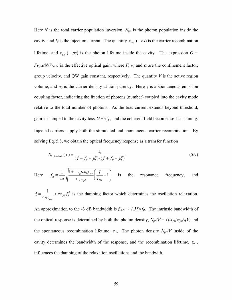
59
Here N is the total carrier population inversion, Nph is the photon population inside the
cavity, and Id is the injection current. The quantity rec (~ ns) is the carrier recombination
lifetime, and ph (~ ps) is the photon lifetime inside the cavity. The expression G =
Γνg(N/V-n0) is the effective optical gain, where Γ, νg and are the confinement factor,
group velocity, and QW gain constant, respectively. The quantity V is the active region
volume, and n0 is the carrier density at transparency. Here γ is a spontaneous emission
coupling factor, indicating the fraction of photons (number) coupled into the cavity mode
relative to the total number of photons. As the bias current extends beyond threshold,
gain is clamped to the cavity loss 1phG , and the coherent field becomes self-sustaining.
Injected carriers supply both the stimulated and spontaneous carrier recombination. By
solving Eq. 5.8, we obtain the optical frequency response as a transfer function
021,intrinsic ( ) .
( ) ( )R R
AS f
f f j f f j
(5.9)
Here 0111
2g ph
Rrec ph TH
v n If
I
is the resonance frequency, and
21
4 ph Rrec
f
is the damping factor which determines the oscillation relaxation.
An approximation to the -3 dB bandwidth is f-3dB ~ 1.55×fR. The intrinsic bandwidth of
the optical response is determined by both the photon density, Nph/V = (I-ITH)ph/qV, and
the spontaneous recombination lifetime, rec. The photon density Nph/V inside of the
cavity determines the bandwidth of the response, and the recombination lifetime, rec,
influences the damping of the relaxation oscillations and the bandwith.
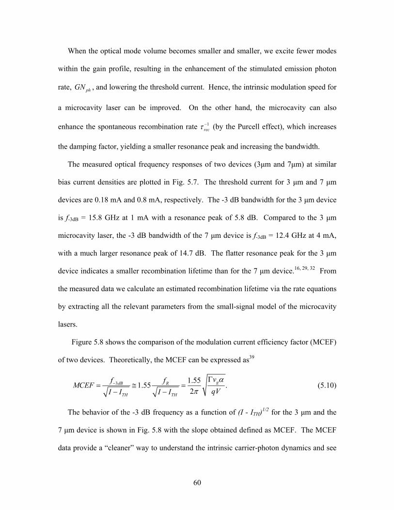
60
When the optical mode volume becomes smaller and smaller, we excite fewer modes
within the gain profile, resulting in the enhancement of the stimulated emission photon
rate, phGN , and lowering the threshold current. Hence, the intrinsic modulation speed for
a microcavity laser can be improved. On the other hand, the microcavity can also
enhance the spontaneous recombination rate 1rec (by the Purcell effect), which increases
the damping factor, yielding a smaller resonance peak and increasing the bandwidth.
The measured optical frequency responses of two devices (3μm and 7μm) at similar
bias current densities are plotted in Fig. 5.7. The threshold current for 3 μm and 7 μm
devices are 0.18 mA and 0.8 mA, respectively. The -3 dB bandwidth for the 3 μm device
is f-3dB = 15.8 GHz at 1 mA with a resonance peak of 5.8 dB. Compared to the 3 μm
microcavity laser, the -3 dB bandwidth of the 7 μm device is f-3dB = 12.4 GHz at 4 mA,
with a much larger resonance peak of 14.7 dB. The flatter resonance peak for the 3 μm
device indicates a smaller recombination lifetime than for the 7 μm device.16, 29, 32 From
the measured data we calculate an estimated recombination lifetime via the rate equations
by extracting all the relevant parameters from the small-signal model of the microcavity
lasers.
Figure 5.8 shows the comparison of the modulation current efficiency factor (MCEF)
of two devices. Theoretically, the MCEF can be expressed as39
3 1.551.55 .
2gdB R
TH TH
vf fMCEF
qVI I I I
(5.10)
The behavior of the -3 dB frequency as a function of (I - ITH)1/2 for the 3 μm and the
7 μm device is shown in Fig. 5.8 with the slope obtained defined as MCEF. The MCEF
data provide a “cleaner” way to understand the intrinsic carrier-photon dynamics and see

61
how it relates to the effect of the optical volume. Compared to the “bulk” laser without
any enhancement of rec, the 3 μm microcavity laser has a MCEF = 17.47 GHz/mA1/2,
which is 2.5 times more efficient than the 7 m VCSEL laser with MCEF = 6.76
GHz/mA1/2.
In the method of direct laser modulation, the most important issue is the existence of
the resonance bump, which affects the data transmission integrity of the system. The
resonance peak frequency fR gives rise to “ringing” in the time-domain output waveform
of the laser and limits the available modulation bandwidth. If resonance is present, the
highest data rate is limited by the resonance frequency, fR, due to waveform distortion by
the “overshoot” and “undershoot,” further resulting in a “closed” eye diagram. Without
the resonance bump, the available bandwidth is much improved and determined by f-3dB,
which is easily observed in the modulation of a transistor laser.32 Besides an increase in
the maximum transmittable data rate, resonance-free operation leads also to better signal
quality, which can be shown by an eye diagram measurement. We use an Agilent N4901
Serial BERT to generate a 13.5 Gbit/s (equipment limited) NRZ 27-1 bit-length
pseudorandom binary series pattern, and an Agilent 86100 DCA high-speed wideband
oscilloscope to record the actual eye diagram.
A large signal modulation eye diagram measurement is different from the small
signal frequency response behavior. Devices with higher frequency bandwidth cannot
guarantee the larger data transmission rate and better integrity of an eye diagram. To
illustrate this point, in Fig. 5.9 we compare eye diagrams at 10 Gb/s without filtering
process for a 3 μm microcavity laser at the bias of 0.5 mA and a poorer 7 μm “bulk”
reference device at a bias of 4 mA. In Fig. 5.7 we show that the 7 μm device at 4 mA has

62
a larger bandwidth (~ 12.4 GHz) but also higher resonance peak (~ 14.7 dB) than the
3μm device at 0.5 mA (~ 9.8 GHz with only a 6 dB resonance peak). Though the -3 dB
bandwidth is larger for the former, its larger resonance peak degrades the eye-diagram
integrity. In Fig. 5.9 the 3 μm microcavity device has a smaller signal distortion at the
sampling instant, a smaller crossover width, as well as a larger open eye. These indicate
that the 3μm microcavity laser has larger signal-to-noise ratio, smaller power
consumption, and a longer time interval for successfully sampling the waveform. It
shows therefore that the larger bandwidth alone cannot give rise to higher data
transmission speed. The resonance peak in the RF response curve plays a crucial role in
limiting the data transmission rate.
To illustrate the mode volume effect on the data transmission rate, we compare (in
Fig. 5.10) the eye diagrams of two devices at a data transmission rate of 13.5 Gb/s
(instrument limited). At similar bias current density, the 3 μm microcavity device
presents a “cleaner” eye diagram compared to the degraded eye diagram of the 7 μm
device. Again, this is owing to the large resonance peak (~ 15 dB) in the response curve
of the 7 μm device at 4 mA, which causes the large “overshoot” and “undershoot” and
leads to the eye diagram closure. The eye diagram comparison shows clearly that the
smaller optical mode volume is of benefit for a higher data transmission speed owing to
the smaller carrier spontaneous lifetime and the larger damping factor of a higher Q
microcavity. In contrast, for the larger “bulk” reference device and multimode operation,
higher bias current and carrier injection (thus higher photon density Nph) is required and
more power consumption to extend the bandwidth and reduce the resonance peak.

63
5.4 Microwave Small-Signal Model
The measured microcavity laser microwave bandwidth to determine the optical
response is not only dependent on the ideal intrinsic device bandwidth, but also is
influenced by extrinsic device parasitic electrical parameters. We show in Fig. 5.11 the
schematic microcavity device cross section with all the related extrinsic parasitic
parameters. The intrinsic device region enclosed by the red-dashed rectangle is the
intrinsic forward biased junction resistance Rj and diffusion capacitance Cdiff. The pad
extrinsic elements Cp and Rp are the contact pad capacitance and resistance. The
semiconductor extrinsic elements Rs and Rn are the DBR mirror resistances. The
semiconductor parasitic capacitance Ca is the sum of series Cox and Cdep, oxide and
junction depletion capacitances.
From two-port network theory, we can express the reflection coefficient, S11, and
transfer function, H ext ( f ), as
11
( ) ( ) ( ),
( ) ( )tot tot tot
tot tot
i f i f i fS
i f i f
(5.11)
and
11
( ) ( )( ) 1 ,
( ) ( )d d
exttot tot
i f i fH f S
i f i f (5.12)
where ( )toti f is the incident current wave and ( )toti f is the reflected current wave. The
total modulation current from the probe at frequency f is ( ) ( ) ( )tot tot toti f i f i f , and id(f)
is the small-signal modulation current through the intrinsic diode region at the same
frequency. By fitting of S11, we can extract all the parasitic parameters as listed in Table
5.4. We find that the major contribution to signal time delay causing bandwidth
64
limitations arises from the junction diffusion capacitance, which is proportional to the
device aperture area and current density.
In order to obtain the intrinsic modulation bandwidth to then determine the
recombination lifetime for a microcavity laser based on the rate equations, we have to
subtract the parasitic contributions. Thus, the overall frequency modulation response can
be expressed as
21,intri21,o nsia cver ll
( ) ( )( )( ) ( ) ( ).
( ) (·
) ( )ph phd
exttot tot d
N f N fi fS f f f
i f i fH
i fS (5.13)
The first term is the external parasitic transfer function, which characterizes the
efficiency of delivery of the microwave signal to the intrinsic active region. The second
term is the intrinsic part of the transfer function, which determines the efficiency of the
photon modulation based on the input electrical signal to the active region. This term is
also the same as shown in Eq. (5.9), and can be written as
021,intrinsic ( ) .
( ) ( )R R
AS f
f f j f f j
(5.9)
From fitting of the microwave S11 parameter at different bias points, we extract the
required parameters and obtain the extrinsic transfer function H ext ( f ). These can be
subtracted from the measured data to get the intrinsic response behavior S21, intrinsic. The
extrinsic transfer function Hext(f) depends on the device layout structure, operating
frequencies, and bias currents. Large input impedance mismatch of the 3 m microcavity
laser causes higher reflection of the input signal at the low frequency range. Transmitted
microwave signal to the intrinsic part of the device (Fig. 5.11) increases gradually with
input frequency owing to more impedance match (to 50 ) resulting from the capacitance
effect. To obtain the intrinsic Nph vs. Id behavior we fit the resonance frequency

65
0111
2g ph
Rrec ph TH
v n If
I
and damping parameter 21
4 ph Rrec
f
for each bias
current, and extract the recombination lifetime and the photon lifetime, which are rec =
0.4 ns and ph = 4.2 ps for the 3 m diameter microcavity device, and rec = 0.82 ns and
ph = 4.8 ps for the 7 m device. For the 3 m microcavity laser the “enhanced” (reduced)
recombination lifetime changes from the usual 0.82 ns reference value to the reduced
value 0.4 ns, or Purcell factor, Fp ~ 2. The microwave method described here for
determination of carrier lifetime is consistent with previous spectral analyses, e.g., for the
dA = 3.5 m device giving an Fp ~ 1.5 (see Table 5.2). The microwave method of
measurement has the advantage of being simpler and more efficient in separating input
and output signals since it employs an electrical-input and optical-output, and no complex
optical-to-optical pump-probe time-resolved techniques.
The small-signal model employed here can also provide comprehensive information
on device parameters for layout design and process optimization to enhance the optical
modulation bandwidth. Figure 5.12 shows the measured optical response curves, S21, of
the 3 m microcavity laser and the corresponding model shows curves fitted to the
measured data. The model projected curves with a reduced device parasitic capacitance
and resistance are also plotted in Fig. 5.12. With the reduction of the parasitics from the
actual devices (e.g., pad capacitance Cp to Cp/4, parasitic capacitance Ca to Ca/4, and
resistances Rn + Rs to (Rn + Rs)/2), the optical modulation bandwidth for the 3 m
microcavity laser is expected to improve to ~ 20 GHz for I = 1 mA. The projected
(enhanced) bandwidths of the 3 m and the 7 m devices at three bias currents are listed

66
in Table 5.4. With still more refined process steps and layout design, the optical
microwave performance can be further improved.
We show that for a microcavity laser the recombination rate can be enhanced by the
Purcell effect (~ 2×), but is still only a limited cavity improvement. The device is still
limited by charge storage and photon-charge resonance. Recently, however, the tilted-
charge operation of a transistor laser has manifested a fast extrinsic spontaneous
recombination lifetime (rec ~ 26 ps), compared to the diode laser case of ~ 1 ns.
Intrinsically the transistor laser can have a much larger bandwidth and flat frequency
response owing to the “fast” collector removal of slower-recombining carriers.32
Concluding, we have presented DC and RF measurement data on QW
microcavity lasers showing the effect of the cavity volume on the device performance.
We demonstrate that as the optical volume is shrunk, the mode spacing and Purcell
enhancement factor increase. With higher cavity Q and a faster spontaneous emission
rate, laser threshold ITH is lower and the side-mode suppression ratio (SMSR) larger.
Simultaneously the intrinsic frequency-modulation bandwidth above threshold will
increase due to the higher photon density and faster spontaneous recombination rate. In
addition, a “fast” spontaneous emission rate (smaller lifetime) gives “fast” damping and a
tendency to resonance-free response in high frequency modulation, thus improving the
data bit error rate and eye-diagram quality in high-speed data transmission. With respect
to low power consumption and high data transmission speed, a microcavity laser design
is useful for short distance optical communication. The threshold current of a smaller
volume microcavity laser is less sensitive to temperature owing to the greater carrier
concentration in the fundamental mode. On the other hand, a smaller volume suffers

67
more from the greater heat generation at a given current density, as well as a larger
wavelength shift, which is not desired for reliable optical communications.
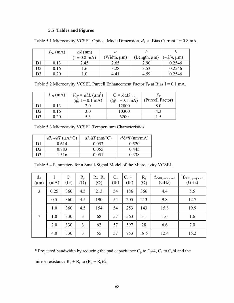
68
5.5 Tables and Figures
Table 5.1 Microcavity VCSEL Optical Mode Dimension, d0, at Bias Current I = 0.8 mA.
(mA) nmm
a (Width, m)
b (Length, m)
L (~ñ, m)
D1 0.13 2.45 2.65 2.90 0.2546 D2 0.16 1.6 3.28 3.53 0.2546 D3 0.20 1.0 4.41 4.59 0.2546
Table 5.2 Microcavity VCSEL Purcell Enhancement Factor FP at Bias I = 0.1 mA.
ITH (mA) Veff = abL (m3) (@ I = 0.1 mA)
Q = cav (@ I =0.1 mA)
FP (Purcell Factor)
D1 0.13 2.0 12800 8.0 D2 0.16 3.0 10300 4.3 D3 0.20 5.3 6200 1.5
Table 5.3 Microcavity VCSEL Temperature Characteristics.
dITH/dT (A/oC) ddT (nm/oC) ddI (nm/mA) D1 0.614 0.053 0.520 D2 0.883 0.055 0.445 D3 1.516 0.051 0.338
Table 5.4 Parameters for a Small-Signal Model of the Microcavity VCSEL.
dA (m)
I (mA)
Cp (fF)
Rp ()
Rn+Rs ()
Ca (fF)
Cdiff (fF)
Rj ()
f-3dB, measured (GHz)
*f-3dB, projected (GHz)
0.25 360 4.5 213 54 186 366 4.4 5.5
0.5 360 4.5 190 54 205 213 9.8 12.7
3
1.0 360 4.5 154 54 253 143 15.8 19.9
1.0 330 3 68 57 563 31 1.6 1.6
2.0 330 3 62 57 597 28 6.6 7.0
7
4.0 330 3 55 57 753 18.5 12.4 15.2
* Projected bandwidth by reducing the pad capacitance Cp to Cp/4, Ca to Ca/4 and the
mirror resistance Rn + Rs to (Rn + Rs)/2.

69
Fig. 5.1 (i) Schematic cross-section of UIUC microcavity VCSEL device. (ii) Microcavity schematic diagram showing the allowed optical modes: (a) 1st order mode, (b) 2nd order mode, and (c) 3rd order mode.
Fig. 5.2 L-I and I-V curves for three different diameter microcavity lasers at 25 oC. The aperture sizes for the three devices are: dA = 2 μm for D1, dA = 2.5 μm for D2, and dA = 3.5 μm for D3.

70
Fig. 5.3 Optical spectra of a microcavity VCSEL device (ITH = 0.13 mA) at different bias currents. The fundamental mode is labeled (a) (shown in Fig. 5.1), and the 2nd order mode (b) at 2.45 nm longer wavelength and 32.5 dB suppression. The 3rd order mode intensity is too weak to be recorded.
Fig. 5.4 Side mode suppression ratio (SMSR) vs. bias current for three different microcavity VCSEL devices: (1) D1 with mode spacing (MS) Δλ ~ 2.45 nm, (2) D2 with Δλ ~ 1.6 nm, and (3) D3 with Δλ ~ 1.0 nm. The smaller the aperture, the larger Δλ and the smaller the threshold current, as well as the larger the SMSR slope before lasing.
71
Fig. 5.5 Temperature dependence of the L-I-V curves for the D2 (dA = 2.5 μm) microcavity laser.
Fig. 5.6 Microcavity laser fundamental mode wavelength, λ(1,1), versus injection current for D2 device (dA = 2.5 μm) at different temperatures ranging from 15 oC to 40 oC. The measured dλ/dT is 0.055 nm/oC and dλ/dI is 0.445 nm/mA.

72
Fig. 5.7 Frequency response of 3 m and 7 m microcavity VCSEL devices at various bias currents: (a) 3 m device biased at current I = 0.25, 0.5, 1 mA, and -3 dB bandwidth f-3dB = 15.8 GHz at 1 mA with resonance peak of 5.8 dB. (b) 7 m device at various bias currents, and -3 dB bandwidth f-3dB = 12.4 GHz at 4 mA with resonance peak of 14.7 dB.
Fig. 5.8 A -3 dB frequency (f-3dB) versus (I-ITH)1/2 comparison of 3 m and 7 m microcavity lasers. The slope for the modulation current efficiency factor (MCEF) is 17.47 and 6.76 GHz/mA1/2 for the 3 m and 7 m devices, respectively.

73
Fig. 5.9 Eye diagrams of 3 m and 7 m microcavity lasers at 10 Gb/s: (a) 3 m aperture diameter device at bias current 0.5 mA; (b) 7 m aperture diameter device at bias current I = 4 mA.
Fig. 5.10 Eye diagrams of 3 m and 7 m microcavity lasers at 13.5 Gb/s: (a) 3 m aperture diameter device at bias current 1 mA; (b) 7 m aperture diameter device at bias current I = 4 mA.

74
Fig. 5.11 Typical diode VCSEL microcavity lasers with the equivalent intrinsic and extrinsic RC parameters identified as follows: Rj, junction resistance; Cdep, depletion capacitance; Cdiff, diffusion capacitance; Rs, p-type DBR series resistance (with oxide confinement); Rn, n-type DBR series resistance (without oxide confinement); Cp and Rp are the extrinsic pad capacitance and resistance. Ca is the series capacitance of Cox and Cdep for modeling convenience. The intrinsic part of the laser operation is identified by the dashed line (red) rectangle.
Fig. 5.12 Measured optical response, S21, of 3 m aperture diameter microcavity laser and model fitting as well as the model projected optical response f-3dB ~ 20 GHz with a reduced device parasitic capacitance Cp/4, and resistances (Rn+Rs)/2.

75
6. CONCLUSION
It is shown that un-doped quantum wells (QWs) embedded in the base region of a
heterojunction bipolar transistor (HBT) structure can enhance the light output and reduce
experimentally, under dynamic tilted-charge boundary condition, the effective carrier
recombination lifetime of injected minority carriers in the base region as an improved
novel high-speed optical device—the light-emitting transistor (LET). A unique three-
terminal electrical and optical characteristic of the LET offers a promising method for
photonics integration and short-range optical transmitter and interconnect.
The enhanced recombination rate and reduced recombination lifetime of a LET is
demonstrated by simultaneously operating multi-GHz electrical and optical signal output
through a common-collector device design, resulting in a better matched impedance (50
Ω) owing to reverse-biased base-collector junction as an rf signal input terminal. The
effective recombination lifetime, corresponding to the optical spontaneous modulation
bandwidth f3dB, is reduced (i.e., bandwidth is enhanced) by laterally scaling the extrinsic
parasitic part of an oxide-confined aperture LET. With a smaller aperture and an
increased intrinsic portion, the light output as well as the electrical gain (= IC/IB) of
an LET are improved.
Inherited from a common-collector design of LET, a tilted-charge LED is proposed by
incorporating a “drain” layer underneath the QW-embedded base region to “drain away”
excessive slow-recombining carriers with a reverse built-in field at base-“drain” junction
maintained by a common potential obtained via a common contact metallization design.
The zero base-“drain” potential difference ensures that there is no base charge population
density at the base-“drain” boundary, hence establishing a dynamic “tilted” emitter-to-

76
“drain” population in the base. The “drain” layer performs therefore a role similar to the
collector in a three-terminal LET. Base carriers in transit from the emitter to the “drain”
that do not recombine within the base transit time are removed, or “drained.” This
enables fast modulation of the tilted-charge LED by preventing the build-up of “slow”
charge in the base. The tilted-charge LED possesses the high speed optical modulation
characteristics of a LET.
Microcavity light-emitting devices with reduced spontaneous recombination lifetimes
(faster band-to-band recombination) are of great interest in the pursuit of threshold-less
lasers and LEDs for potential use in optical communications at high modulation speed.
Some reduced spontaneous lifetime, < 500 ps (~ 2 x lower than bulk values, ~ 1 ns), is
observed in the Purcell effect in which the upper-state to lower-state transition rate is
enhanced by a high-Q microcavity of reduced optical mode density. A sensitive
microwave method has been used to characterize a quantum-well vertical cavity surface
emitting laser (dA ~ 3 m aperture, ITH = 0.18 mA) exhibiting almost single-mode
operation and 2.08 times reduction in electron-hole spontaneous lifetime (enhanced
recombination rate) by the Purcell effect. By studying the optical microwave frequency
response of microcavity VCSELs in the transition from spontaneous to coherent
operation, we resolve the dynamics of electron-hole recombination (spontaneous to
stimulated) and reveal the existence of “fast” spontaneous recombination lifetime (~ 150
ps) in a carrier population generally characterized by a large average lifetime of ~ 1 ns.
Via the three-terminal heterojunction bipolar transistor laser and its “tilted” base
charge, a pinned non-floating source of recombination because of the zero-charge
boundary condition at the reverse-biased collector junction, we have also recently

77
identified an even faster spontaneous lifetime of < 25 ps (~ 40 times reduction from bulk
values). It clearly is possible with the choice of the microcavity device geometry and the
cavity boundary conditions to favor the faster carrier recombination process (reduced
recombination lifetime) to enhance high speed direct modulation of a semiconductor laser.
The demand for faster laser speeds is propelled by the increasing demands for next
generation high-speed data communication (100 Gbit Ethernet and more), high
bandwidth interconnects for data centers and high-throughput, high-density interconnects
in high performance computing systems. From previous experimental results presented
in this work, we demonstrated the world-record speed for spontaneous bandwidth
modulation of the HBLET, as well as the subsequent tilted-charge LED. Because of their
short spontaneous recombination lifetime (23 ps), though limited by extrinsic parasitics,
in conjunction with stimulated enhancement due to proper cavity design, ultra-fast,
resonance-free vertical-cavity transistor lasers (VCTLs) can serve in applications for the
next generation of optical interconnects, fiber communication systems, and opto-
electronic integrated circuits.

78
REFERENCES 1 R. N. Hall, G. E. Fenner, J. D. Kingsley, T. J. Soltys, and R. O. Carlson, Phys. Rev. Lett. 9,
366 (1962).
2 N. Holonyak, Jr. and S. F. Bevacqua, Appl. Phys. Lett. 1, 82 (1962).
3 M. I. Nathan, W. P. Dumke, G. Burns, F. H. Dill, Jr., and G. Lasher, Appl. Phys. Lett. 1, 62
(1962).
4 T. M. Quist, R. H. Rediker, R. J. Keyes, W. E. Krag, B. Lax, A. L. McWhorter, and H. J.
Zeiger, Appl. Phys. Lett. 1, 91 (1962).
5 J. J. Wierer, D. A. Kellogg, and N. Holonyak, Jr., Appl. Phys. Lett. 74, 926 (1999).
6 C. H. Chen, M. Hargis, J. M. Woodall, M. R. Melloch, J. S. Reynolds, E. Yablonovitch, and
W. Wang, Appl. Phys. Lett. 74, 3140 (1999).
7 M. Feng, N. Holonyak, Jr., and W. Hafez, Appl. Phys. Lett. 84, 151 (2004).
8 M. Feng, N. Holonyak, Jr., and R. Chan, Appl. Phys. Lett. 84, 1952 (2004).
9 W. Snodgrass, B. R. Wu, K. Y. Cheng, and M. Feng, IEEE Intl. Electron Devices Meeting
(IEDM), pp. 663-666 (2007).
10 M. Feng, N. Holonyak, Jr., G. Walter, and R. Chan, Appl. Phys. Lett. 87, 131103 (2005).
11 G. Walter, N. Holonyak, Jr., M. Feng, and R. Chan, Appl. Phys. Lett. 85, 4768 (2004).
12 R. Chan, M. Feng, N. Holonyak, Jr., A. James, and G. Walter, Appl. Phys. Lett. 88, 143508
(2006).
13 M. Feng, N. Holonyak, Jr., A. James, K. Cimino, G. Walter, and R. Chan, Appl. Phys. Lett.
89, 113504 (2006).
14 H. W. Then, M. Feng, N. Holonyak, Jr., and C. H. Wu, Appl. Phys. Lett. 91, 033505, 2007.
15 G. B. Stringfellow and M. G. Craford, eds., in High Brightness Light Emitting Diodes,
Semiconductors and Semimetals, (Academic Press, San Diego, CA, 1997), Vol. 48, p. 56.
16 M. Feng, N. Holonyak, Jr., H. W. Then, and G. Walter, Appl. Phys. Lett. 91, 053501 (2007).
79
17 T. J. de Lyon, J. M. Woodall, D. T. McInturff, P. D. Kirchner, J. A. Kash, R. J. S. Bates, R. T.
Hodgson, and F. Cardone, Appl. Phys. Lett. 59, 22-24 (1991).
18 H. Grothe, W. Proebster, and W. Harth, Electron. Lett. 15, 702-703 (1979).
19 X. Guo and E. F. Schubert, Appl. Phys. Lett. 78, 3337-3339 (2001).
20 E. M. Purcell, Phys. Rev. 69, 681 (1946).
21 L. A. Graham, D. L. Huffaker, Q. Deng, and D. G. Deppe, Appl. Phys. Lett. 72, 1670 (1998).
22 L. A. Graham, D. L. Huffaker, and D. G. Deppe, Appl. Phys. Lett. 74, 2408 (1999).
23 J. M. Gerard and B. Gayral, J. Lightwave Technol. 17, 2089 (1999).
24 T. Baba and D. Sano, IEEE J. Sel. Top. Quantum Electron. 9, 1340 (2003).
25 S. Maranowski, A. Sugg, E. I. Chen, and N. Holonyak, Jr., Appl. Phys. Lett. 63, 1660 (1993).
26 J. A. Kong, Electromagnetic Wave Theory, (EMW Publishing, Cambridge, MA, 1998), p. 327.
27 Y. Suematsu and K. Furuya, Trans. IEICE Japan 60, 467 (1977).
28 T. Baba, T. Hamano, F. Koyama, and K. Iga, IEEE J. Quantum Electron. 27, 1347 (1991).
29 H. Statz and G. deMars, Quantum Electronics, (Columbia University Press, New York, NY,
1960), p. 650.
30 S. A. Wartenberg, RF Measurements of Die and Packages, (Artech House, Norwood, MA,
2002), p. 124.
31 R. S. Tucker, IEE Proc. 128, 180 (1981).
32 M. Feng, H. W. Then, N. Holonyak, Jr., G. Walter, and A. James, Appl. Phys. Lett. 95,
033509 (2009).
33 H. W. Then, C. H. Wu, M. Feng, and N. Holonyak, Jr., Appl. Phys. Lett. 96, 131107 (2010).
34 M. Kajita, T. Numai, K. Kurihara, T. Yoshikawa, H. Saito, Y. Sugimoto, M. Sugimoto, H.
Kosaka, I. Ogura, and K. Kasahara, Jpn. J. Appl. Phys. 33, 859 (1994).
35 M. Kajita, T. Kawakami, M. Nido, A. Kimura, T. Yoshikawa, K. Kurihara, Y. Sugimoto, and
K. Kasahara, IEEE J. Sel. Top. Quantum Electron. 1, 654 (1995).
80
36 D. B. Young, J. W. Scott, F. H. Peters, M. G. Peters, M. L. Majewski, B. J. Thibeult, S. W.
Corzing, and L. A. Coldren, IEEE J. Quantum Electron. 29, 2013 (1993).
37 S. R. Kisting, P. W. Bohn, E. Andideh, I. Adesida, B. T. Cunningham, G. E. Stillman and T. D.
Harris, Appl. Phys. Lett. 57, 1328 (1990).
38 J. J. Dudley, D. L. Crawford, and J. E. Bowers, IEEE Photonics Technol. Lett. 4, 311 (1992).
39 T. R. Chen, B. Zhao, L. Eng, Y. H. Zhuang, J. O'Brien, and A. Yariv, Electron. Lett. 29, 1525
(1993).