
© 2009 Ning Zhang - UFDC Image Array 2ufdcimages.uflib.ufl.edu/UF/E0/02/42/61/00001/zhang_n.pdfNING...
191
1 CMOS MILLIMETER-WAVE RECEIVER FRONT-END CIRCUITS AND THEIR APPLICATIONS By NING ZHANG A DISSERTATION PRESENTED TO THE GRADUATE SCHOOL OF THE UNIVERSITY OF FLORIDA IN PARTIAL FULFILLMENT OF THE REQUIREMENTS FOR THE DEGREE OF DOCTOR OF PHILOSOPHY UNIVERSITY OF FLORIDA 2009
Transcript of © 2009 Ning Zhang - UFDC Image Array 2ufdcimages.uflib.ufl.edu/UF/E0/02/42/61/00001/zhang_n.pdfNING...

1
CMOS MILLIMETER-WAVE RECEIVER FRONT-END CIRCUITS AND THEIR APPLICATIONS
By
NING ZHANG
A DISSERTATION PRESENTED TO THE GRADUATE SCHOOL OF THE UNIVERSITY OF FLORIDA IN PARTIAL FULFILLMENT
OF THE REQUIREMENTS FOR THE DEGREE OF DOCTOR OF PHILOSOPHY
UNIVERSITY OF FLORIDA
2009

2
© 2009 Ning Zhang

3
To my parents, brother, wife and my beloved baby boy, Raphael Zirui

4
ACKNOWLEDGMENTS
I would like to first thank my advisor, Professor Kenneth K. O, for his constant
encouragement and patient guidance for me through the whole challenging research process. I
would also like to thank Dr. William R. Eisenstadt, Dr. John G. Harris, and Dr. Gloria J. Wiens
for their advices and time commitment in serving on my committee.
Much appreciation goes to National Science Foundation (NSF), Semiconductor Research
Consortium (SRC) and Texas Instrument Incorporation (TI Inc.) for providing funds and access
to advanced CMOS technology for our millimeter-wave research projects. My special thanks go
to Dr. Chih-Ming Hung of TI Inc. for his long-term support of chip design and fabrication, Dr.
Brian Floyd of IBM T.J. Watson Research Center, and Dr Ivan To of Freescale Inc. for assisting
our millimeter wave circuit measurements and answering mm-wave design technical questions.
I have been very fortunate to work with Hsin-Ta Wu and Shashank Nallani in the mm-
wave projects, whose teaching and discussions have speeded up my research. I would also like to
thank all my other former and current colleagues at University of Florida for their time and
extreme patience to answer my questions and share their design insights and hands-on
experience generously with me. Some of their names are listed here: Chuying Mao, Yu Su,
Changhua Cao, Yanping Ding, Swaminathan Sankaran, Kwangchun Jung, Dongha Shim,
Haifeng Xu, Eunyoung Seok, Chikuang Yu, Zhe Wang, Xiaoling Guo, Choongyul Cha, Seon-Ho
Hwang, Myoung Hwang, Wuttichai Levdensitboon, Kyujin Oh, Ruonan Han, Tie Sun, Teyu Kao,
and Chieh-Lin Wu.
I am deeply grateful for my parents, my brother and my wife for their endless love, caring
and encouragement, and the endless happiness my beloved baby boy Raphael Zirui brings me.
This work is dedicated to them all.

5
TABLE OF CONTENTS page
ACKNOWLEDGMENTS ...............................................................................................................4
LIST OF TABLES...........................................................................................................................7
LIST OF FIGURES .........................................................................................................................9
ABSTRACT...................................................................................................................................14
CHAPTER
1 INTRODUCTION ..................................................................................................................16
1.1 Era of Connectivity and Scaling ...................................................................................16 1.2 Introduction to Millimeter-Wave Technologies............................................................20 1.3 Introduction to Device Technologies Supporting Millimeter-Wave ICs......................23 1.4 Organization of the Dissertation ...................................................................................27
2 INTRODUCTION TO DIGITAL CMOS TECHNOLOGY..................................................29
2.1 Nano-Scale Digital CMOS............................................................................................29 2.2 Introduction to the 65-nm Digital Bulk CMOS Process ...............................................36
2.2.1 Transistor Model and Layout Optimization......................................................36 2.2.2 Passive Devices in TI 65-nm Digital Bulk CMOS Process ..............................40
2.2.2.1 Metal-oxide-metal capacitor...............................................................41 2.2.2.2 Metal-oxide-semiconductor capacitor ................................................43 2.2.2.3 Spiral inductor ....................................................................................45 2.2.2.4 Line inductor.......................................................................................48 2.2.2.5 Transformer ........................................................................................53 2.2.2.6 Signal pad ...........................................................................................55
2.3 Summary .......................................................................................................................56
3 CRITICAL CICRUIT BLOCKS OF MILLIMETER-WAVE RECEIVER FRONT-END...58
3.1 Introduction...................................................................................................................58 3.2 Tuned Amplifier............................................................................................................59
3.2.1 Design of 80-GHz Tuned Amplifier .................................................................59 3.2.2 Non-Ideal On-Chip Ground and Supply Network ............................................69 3.2.3 Substrate Coupling............................................................................................76 3.2.4 Measurements of 80-GHz Tuned Amplifier .....................................................77
3.3 Voltage-Controlled Oscillator.......................................................................................84 3.3.1 Design of 94-GHz Voltage-Controlled Oscillator ............................................85 3.3.2 Measurements of 94-GHz Voltage-Controlled Oscillator ................................88
3.4 Down-Conversion Mixer ..............................................................................................91 3.4.1 Design of 77-GHz Down-Conversion Mixer....................................................92

6
3.4.2 Measurements of 77-GHz Down-Conversion Mixer........................................94 3.5 Summary .....................................................................................................................101
4 APPLICATIONS FOR CMOS MILLIMETER-WAVE RECEIVER FRONT-END CIRCUITS ............................................................................................................................102
4.1 Introduction.................................................................................................................102 4.2 Introduction to 77-GHz Automobile Radar ................................................................102 4.3 Overview of the 77-GHz Radar System .....................................................................105 4.4 Design and Measurement of an 80-GHz Down-Converter.........................................108 4.5 Radio Architecture for the 77-GHz Pulsed Radar System..........................................118 4.6 Design of Receiver Chain for the 77-GHz Pulsed Radar Transceiver........................121 4.7 Design of Frequency Generation System for the 77-GHz Pulsed Radar
Transceiver..................................................................................................................126 4.8 Measurements of the Radar Receiver Front-End Integrated with the Frequency
Generation System ......................................................................................................133 4.9 Summary .....................................................................................................................147
5 SUMMARY AND FUTURE WORK ..................................................................................149
5.1 Summary .....................................................................................................................149 5.2 Future Work ................................................................................................................151
APPENDIX: SYSTEM LEVEL STUDY FOR WIRELESS INTERCHIP INTERCONNECT IN MM-WAVE BAND ........................................................................................................153
A.1 Interconnect Bottleneck ..............................................................................................153 A.2 Wireless Interconnect..................................................................................................155 A.3 Wireless Interconnect at 60-80 GHz...........................................................................157 A.4 System Architecture and Specification .......................................................................158 A.5 Low Loss Propagation Path and Efficient Antenna in a Package...............................162 A.6 Initial System Specification and Simple Link Budget Analysis .................................165 A.7 Radio Architecture ......................................................................................................167 A.8 Duplex Scheme and System Architecture Reconsideration........................................171 A.9 Alternate Architecture with Frequency Division Duplex Scheme..............................176 A.10 Summary .....................................................................................................................179
LIST OF REFERENCES.............................................................................................................181
BIOGRAPHICAL SKETCH .......................................................................................................191

7
LIST OF TABLES
Table page 1-1 Some characteristics of emerging wireless technologies in the United States ..................19
1-2 Some mm-wave applications below 100 GHz...................................................................23
2-1 Capacitances of a series of metal-oxide-metal cap. ...........................................................43
3-1 Performance comparisons of CMOS mm-wave low noise amplifiers...............................84
3-2 Performance comparisons of CMOS fundamental mode voltage-controlled oscillators around 94-GHz .................................................................................................91
3-3 Performance comparisons of stand-alone CMOS mm-wave down-conversion mixer....100
4-1 System specification for the proposed 77-GHz pulsed radar system ..............................106
4-2 Pulsed radar system range calculation for long distance detection..................................107
4-3 Pulsed radar system range calculation for short distance detection.................................107
4-4 Component values of the tuned amplifier in the 80-GHz down-converter......................110
4-5 Component values of the pseudo differential mixer in the 80-GHz down-converter......110
4-6 Comparisons of W-band CMOS receivers ......................................................................117
4-7 Estimation of 27.5-GHz local oscillation leakage at the input of 27.5-GHz down-conversion mixer..............................................................................................................125
4-8 Performances of CMOS phase-locked loop above 50 GHz with fundamental VCO. .....138
4-9 Summary of power consumption of the frequency generation system............................139
4-10 Frequency generation performance summary..................................................................140
4-11 Summary of power consumption of the 83-GHz receiver front-end ...............................145
A-1 Some possible solutions for the wire interconnection bottle-neck ..................................154
A-2 Comparison of several low order modulation schemes ...................................................161
A-3 System specification for the frequency division multiple access wireless interconnect system around 60 GHz.....................................................................................................166

8
A-4 Link budget analysis for one wireless I/O path for a FDMA wireless interconnect system operating around 60 GHz.....................................................................................166
A-5 Wireless inter-chip interconnect system specification reflecting the adaptation of FDD scheme.....................................................................................................................179

9
LIST OF FIGURES
Figure page 1-1 “Anywhere” networks connecting our daily life ...............................................................16
1-2 Some representative wireless applications below 6 GHz ..................................................18
1-3 Unlicensed bands assigned around 60 GHz in several countries/regions..........................20
1-4 Atmospheric absorption vs. frequency ..............................................................................21
1-5 Added absorption due to precipitation vs. frequency ........................................................21
1-6 Circuits operating frequency and output power range in modern day semiconductor technologies for high frequency applications ....................................................................26
2-1 Improved fT and NFmin of MOSFETs with CMOS scaling................................................30
2-2 Multiple metal layer stacking structure below protective passivation layer in the back-end of modern nm-range digital bulk CMOS process ..............................................33
2-3 NMOS FET model.............................................................................................................37
2-4 Optimized NMOS FET layout for higher fmax and ro in a TI 65-nm digital bulk CMOS process ...................................................................................................................40
2-5 Metal-oxide-metal capacitor.. ............................................................................................42
2-6 Varactor layouts. ................................................................................................................44
2-7 Spiral inductor....................................................................................................................47
2-8 High frequency structure simulator simulated results for a nominal spiral inductor of ~250 pH. ............................................................................................................................49
2-9 Various line inductor structures. ........................................................................................50
2-10 HFSS simulated results for various line inductor structures (40 m long and 1.6 m wide metal6 line) in Figure 2-9..........................................................................................52
2-11 Baluns. ...............................................................................................................................54
2-12 Simulated |S11| and |S12| of a loop balun tuned to 50 GHz and a line balun tuned to 80 GHz from HFSS two-port simulations. .............................................................................55
2-13 Signal pad structure and its model .....................................................................................56
3-1 Schematic of the 80-GHz 6-stage tuned amplifier.............................................................60

10
3-2 Comparison between common source and cascode 1-stage amplifier around 80 GHz.....61
3-3 CS and cascode amplifier performance sensitivity with device body/substrate resistance............................................................................................................................62
3-4 Stagger tuning of six amplification stages .........................................................................65
3-5 One-stage CS amplifier schematic used to tune frequency and find Sopt to obtain a good tradeoff among power gain, noise figure, and stability. ...........................................66
3-6 ZSopt, availabe power gain circles, noise figure circles and source stability circles around 80 GHz for low noise matching network design. ..................................................67
3-7 Schematic used to design the inter-stage matching networks............................................68
3-8 Parasitics in the current paths including on-chip/off-chip circuits ....................................70
3-9 Schematic of a simplified on-chip ground parasitics network (in dashed box) connecting the sensitive nodes in the tuned amplifier. ......................................................73
3-10 Esitmation of ground parasitics influence on amplifier performance................................74
3-11 Substrate network...............................................................................................................77
3-12 Die photo of the 80-GHz 6-stage tuned amplifier .............................................................78
3-13 S-parameter measurement set-up for the 80-GHz tuned amplifier....................................78
3-14 Measured S-parameters with 1.2 V supply and drained current of 27 mA........................79
3-15 Noise figure measurement set-up for the 80-GHz tuned amplifier....................................80
3-16 Measured power gain and noise figure with 1.2 V supply, bias current 27 mA, and those with 1.5 V supply, bias current 33 mA.....................................................................81
3-17 Linearity measurement set-ups. .........................................................................................82
3-18 W-band signal sources. ......................................................................................................83
3-19 Measured IIP3 and IP1dB of the amplifier under 1.2 V supply and 27 mA drained current.. ..............................................................................................................................83
3-20 Schematic of the 94 GHz voltage-controlled oscillator with all transistors sizes in m...86
3-21 Part of the cross-coupled transistor pair layout with spacings in m. ...............................86
3-22 Inductor and varactor layouts.............................................................................................87
3-23 Die photo of the 94-GHz VCO ..........................................................................................88

11
3-24 Measurement set-up for the 94-GHz VCO ........................................................................89
3-25 Measured VCO output spectrum before de-embedding ....................................................89
3-26 Measured phase noise with 1.5 V and 6 mA VCO core supply with carrier frequency of 94.92 GHz......................................................................................................................89
3-27 Voltage-controlled oscillator tuning curves with 1.5 V supply and bias currents of 2, 4, 6 mA for the VCO core..................................................................................................90
3-28 Schematic of the 77-GHz mixer ......................................................................................942
3-29 Die photo of the 77-GHz mixer .........................................................................................94
3-30 Measured ports matching of the mixer with 1.2 V supply and 5 mA bias current.. ..........95
3-31 Measurement set-up for the 77-GHz mixer conversion gain.............................................95
3-32 Measured conversion gain of the mixer under varying bias currents and LO power levels. .................................................................................................................................96
3-33 Measured average mixer conversion gain (CG), SSB NF and NF after de-embedding RF input balun loss (NF2). .................................................................................................97
3-34 Measurement set-up for the 77-GHz mixer NF. ................................................................97
3-35 Measurement set-up for the 77-GHz mixer IIP3 and IP1dB. ...............................................98
3-36 Measured IIP3 with two input tones of 76.3 and 76.31 GHz and IP1dB with an input at 76.3 GHz under 1.2 V supply and 5 mA drain current. .....................................................98
3-37 Measurement set-up for the 77-GHz mixer LO-RF leakages............................................99
3-38 Measured leakages among mixer ports at VDD=1.2 V and 5 mA drain current.................99
4-1 Vehicle with multiple radar modules for various functions to make driving more safe and comfortable ...............................................................................................................103
4-2 Multi-beam antenna and its radiation pattern for the proposed 77-GHz CMOS radar system ..............................................................................................................................105
4-3 Schematic of the tuned amplifier in the 80-GHz down-converter. ..................................109
4-4 Schematic of the pseudo differential mixer in the 80-GHz down-converter. ..................109
4-5 Die photo of the 80-GHz down-converter. ......................................................................112
4-6 Measured and simulated impedance matching of the down-converter............................114

12
4-7 Measured conversion gain and NF of the down-converter for fixed local oscillation frequency of 60 GHz........................................................................................................115
4-8 Measured conversion gain of the down-converter at varying power levels of the 60-GHz LO delivered to the LO port. ...................................................................................115
4-9 Measured IIP3 and IP1dB of the down-converter at 81 GHz. ...........................................116
4-10 Measured LO-RF and LO-IF leakages of the down-converter. .......................................116
4-11 Simplified block diagram of the CMOS heterodyne radar transceiver showing the LO frequencies generation scheme and separate on-chip dipole antennas for TX and RX...118
4-12 Receiver block diagram showing the main 25.5-GHz LO leakage paths ........................119
4-13 Three-dimension modeling of the transition from the 76.5-GHz on-chip dipole feed to the waveguide section of a high gain antenna .............................................................120
4-14 Receiver mm-wave front-end schematic (RF stages) of the 77-GHz radar system.........122
4-15 Receiver IF and BB stages schematic of the 77-GHz radar system ................................123
4-16 Block diagram of the 51-GHz PLL frequency synthesizer (in dash box) in the proposed 77-GHz radar transceiver .................................................................................126
4-17 Latch-biased static frequency divider used for the 1st and 2nd stage of divider.. .............128
4-18 Simulated input sensitivity plot of the 1st latch-biased static frequency divider. ............131
4-19 Die photo of the 77-GHz radar frequency generation system. ........................................134
4-20 Measurement set-up for the 77-GHz radar frequency generation system. ......................135
4-21 Frequency tuning and single-ended output power of VCO and offset mixer after de-embedding the measurement set-up loss..........................................................................135
4-22 Spectrum of the phase-locked loop 55.5 GHz output ......................................................136
4-23 Phase noise of the PLL 55.5 GHz output.........................................................................137
4-24 Up-converted 83.3 GHz spectrum at the offset mixer output corresponding to 55.5 GHz output of the PLL ....................................................................................................137
4-25 Phase noise at 1 MHz offset and reference spur. .............................................................138
4-26 Die photos of the . ............................................................................................................141
4-27 Measurement set-up for the receiver front-end................................................................142

13
4-28 Measured and simulated input matching |S11| of the receiver front-end..........................143
4-29 Measured and simulated conversion gain and SSB NF of the receiver front-end. ..........144
4-30 Measured IIP3 and IP1dB of the receiver front-end...........................................................145
A-1 Wireless interconnects help reduce multi-chip package area and I/O wiring complexity........................................................................................................................156
A-2 Architecture of an frequency division multiple access wireless inter-chip interconnection system.....................................................................................................160
A-3 Multiple chips/components in an multi-chip module ......................................................162
A-4 Enhanced wave propagation environment for an MCM..................................................163
A-5 HFSS simulated input return loss of a bond wire antenna around 60 GHz. ....................164
A-6 A series of bond wire antenna test structures consisting of silicon chips, gold bond wires and bond pads on FR-4 board. ...............................................................................164
A-7 Measured antenna pair gains of bond wire antennas with and without metal cover. ......165
A-8 Radio circuit architectures. ..............................................................................................169
A-9 A bilateral wireless FDMA interconnect in time division duplex scheme is realized with three RF transceivers and bond wire antennas on each chip ...................................171
A-10 Adjacent bond wire antenna coupling causes serious adjacent channel interference problem and degrades received signal SNR. ...................................................................172
A-11 Adjacent bond wire antenna coupling causes serious reciprocal mixing problems and degrades received signal SNR .........................................................................................174
A-12 An alternative wireless FDMA interconnect architecture increases hardware sharing and mitigates undesirable bond wire antenna coupling. ..................................................175
A-13 Wireless FDMA interconnect system using an FDD scheme utilizes two frequency bands for bidirectional communication, removes the T/R switch and reduces undesirable bond wire antenna coupling..........................................................................177
A-14 Multiple buffers, notch filters and offset mixers can be added to the 60-GHz band frequency synthesizer in Figure A-8 (B) to generate the 80-GHz band LO signals needed by the FDD scheme .............................................................................................178

14
Abstract of Dissertation Presented to the Graduate School of the University of Florida in Partial Fulfillment of the Requirements for the Degree of Doctor of Philosophy
CMOS MILLIMETER-WAVE RECEIVER FRONT-END CIRCUITS AND THEIR
APPLICATIONS
By
Ning Zhang
August 2009
Chair: Kenneth K. O Major: Electrical and Computer Engineering.
The improvement of high frequency capability for silicon devices has made
implementation of millimeter-wave (mm-wave) silicon integrated circuits operating at 60 GHz,
77 GHz and even higher feasible. This had led to the proposal of a low-cost 77-GHz CMOS
transceiver for automobile radar application and a 60-GHz wireless inter-chip interconnect
system. This Ph.D work demonstrated an 80-GHz mm-wave receiver chain integrated with a
frequency synthesizer fabricated using low leakage transistors of a low cost 65-nm bulk CMOS
technology.
An 80-GHz single-ended low noise amplifier (LNA), a 77-GHz down-conversion mixer
and a 94-GHz voltage-controlled oscillator (VCO) have been separately demonstrated. A 1.2-V
supply, the single-ended LNA exhibits 12-dB gain and 9-dB noise figure (NF) consuming 32-
mW power. The mixer has –8-dB conversion gain and 17 dB NF while consuming only 6-mW
power. With a 1.5 V supply, the VCO achieves 5.8% tuning range around 94 GHz and –
87dBc/Hz phase noise at 1 MHz offset while consuming 14-mW power. These designs
demonstrate that the low-cost, low leakage CMOS process can be used for the design of mm-
wave circuit blocks and potentially larger integrated system despite the challenges of using the

15
technology such as low voltage headroom, moderate metallization performance and strict metal
density filling requirements.
An 80-GHz down-converter including an LNA and a mixer is demonstrated. It achieves
16-dB conversion gain and 9-dB noise figure, consuming 52-mW power from a 1.2-V supply. To
build a more complete radar receiver system, a signal generation system using a phase lock loop
is demonstrated. It generates 55 to 60 GHz and 27.5 to 30 GHz LO signals for the receiver down-
conversion, and 83 to 90 GHz carriers for the transmitter. The signal generation system
consumes ~170 mW power with the supplies of 1.2 and 1.4 V. This work has shown that the
low-cost CMOS technology can be used to build wide-locking range, low phase noise and low
power consumption mm-wave signal generation circuits.
Finally, a receiver chain is integrated with the frequency generation system to demonstrate
a radar receiver. The receiver chain starts with an 80 GHz LNA using an on-chip balun to
convert single-ended input signal to differential, a mixer following the LNA down-converts the
incoming signal at 80-GHz to 27-GHz, then an IF amplifier and passive mixer amplify and
down-convert the 27-GHz signal to baseband. Lastly the baseband signal is high-pass filtered
and output to an external load through a source follower buffer. With 1.4/1.2 V power supplies
and LO’s generated on-chip, the receiver circuit has about 7-dB conversion gain, and NF is as
low as 13.8 dB. The IP1dB and IIP3 are –21 and –12 dBm, respectively. The goal of this research
is fulfilled. We successfully demonstrate the feasibility of realizing a low-cost single chip mm-
wave transceiver for automobile radar applications at 77 GHz and beyond.

16
CHAPTER 1 INTRODUCTION
1.1 Era of Connectivity and Scaling
Thanks to the rapid progress of electronics, computer and network technologies in the past
50 years or so, we are now living in an electronic information age. All information is digitized
and spreaded through a global network formed by numerous optical/coaxial backbone,
microwave and satellite relay and cellular/ad-hoc access. Data connection, from long distance to
local area network (LAN) [1], and lately personal area network (PAN) [2] and body area network
(BAN) [3], is interwoven with people’s daily life, providing convenience and productivity
enhancement. Figure 1-1 is an illustration for this “anywhere” connection.
Figure 1-1. “Anywhere” networks connecting our daily life
Observing the development of integrated circuits (IC) industry in the background of the
electronic information age, we see that user demands, market volume, technology investment

17
and development closely couple with each other, forming a positive feedback loop: User
demands and existing needs stimulate capitalists and engineers to look for technical solutions,
huge return/loss prepare people for a cycle of “problems and solutions.” On the other hand,
technology breakthroughs lead to ideas for new applications and commercialization. This is the
driving force for the advancement of the whole electronics industry. Particularly, it has fueled the
Moore’s law, which has become the gauge for electronics to measure the pace of very large scale
integration (VLSI) integrated circuits technology evolution [4].
Users always look for cheaper and faster data services and more functions in a smaller
device. This thirst drives for faster computation, larger storage and wider communication
bandwidth [5], pushing the whole electronics industry to take every possible means to
continuously lower design/manufacture cost of product while squeeze in more functions. Thanks
to these efforts in material/process and circuit architecture/topology innovations, and relentless
scaling-down of semiconductor device technology feature sizes, now we posses relatively low-
cost microprocessors with clock rate of GHz [6], Giga-bytes memory [7] and Giga-bps wireline
communication ICs [8]. However, the bottleneck of communications still exists particularly in
the area of wireless communication and multi-GHz rate interconnects such as processor-to-
processor or processor-to-memory. This bottleneck also explains the proliferation of research
activities in the area of wireless/wireline ICs in the past 20 years or so. The commercially
available cellular phone system-on-a-chip (SOC) with multi-mode, multi-band, self-calibrated,
digitally assisted RF/analog circuitry exemplifies one of the latest efforts and directions of the
wireless communication IC industry, which was still just a concept 10 years ago [9], [10]. The
ever-increasing sampling speed of analog-to-digital conversion and the concept of transforming
the voltage domain signal processing to time domain processing [11], [12] could ultimately lead

18
to the true software-defined-radio (SDR) [13] that could change the function of an extremely
versatile communication hardware platform in a blink of software program loading.
Due to the mobility, flexibility and relatively easy, cheap deployment it brings, wireless
communication technology has become an indispensable part of the global data network and a
significant portion of the global electronics industry [14], [15]. This has let to a need for high-
speed wireless technology. However, to attain a wireless link with data rates of ~100 Mbps-1
Gbps and beyond, there are two fundamental obstacles that must be overcome.
Figure 1-2. Some representative wireless applications below 6 GHz
The first one is the available communication bandwidth for wireless applications.
Nowadays, it is a global norm for governmental organizations to assign or license limited
frequency spectrum to different services/applications. Use of the spectrum in a manageable
fashion avoids chaos and mutual interferences. However, multiple factors such as the availability
of low-cost technology, lower propagation path loss, industrial expertise and investment
accumulation make the spectrum below 6 GHz already packed with all sorts of consumer

19
applications with a variety of communication distance and information rate [16], [17]. Wireless
local-area-network (WLAN) and cellular phone are probably the two examples that many people
have experienced. Figure 1-2 shows a diagram for some representative applications below 6
GHz. The maximum data rates of all these applications may be ultimately limited by the narrow
bandwidths they are assigned and the strong interferences they mutually cause. Several technical
solutions have been proposed to circumvent these issues [18]: ultra-wide-band (UWB)
technology, cognitive radio and mm-wave technology (frequencies from 30 GHz to 300 GHz).
Table 1-1 summarizes typical characteristics of these technologies in USA. Among them, UWB
and mm-wave both can satisfy the need for moderate-to-high data rate applications. UWB faces
the challenges of stricter transmitting power level control and existence of strong narrow-band
interferences from other applications in the populated band. These limit UWB to short distance
(<10 m) applications. On the other hand, mm-wave systems have larger available spectrum
resources worldwide that are relatively clean since fewer applications exist there presently, and
the transmission power level can be much higher than UWB [16]. Millimeter-wave transceiver
modules for Gbps point-to-point communication for ~1 km range are commercially available
[19]. Figure 1-3 shows the much noted 60 GHz unlicensed band spectrum designated in several
developed regions in the world [20]. Such rarely seen global harmony attracts the interest of
industry and it could well be the start of another great success story following the world-wide
acceptance of IEEE 802.11 WLAN.
Table 1-1. Some characteristics of emerging wireless technologies in the United States Technology UWB radio 60 GHz radio Cognitive radio
Spectrum access Underlay Unlicensed Overlay Spectrum (GHz) 0-1 & 3-10 57-64 0-10 Data rate 100-500 Mbps > 1 Gbps 10-100 Mbps Range ~1-10 m ~1 m-1 km ~1 m-10 km

20
Figure 1-3. Unlicensed bands assigned around 60 GHz in several countries/regions
The second obstacle is the need for an affordable semiconductor technology that not only
provides adequate and reliable performances for ~Gbps wireless circuits, but also suits large
volume production and scale of economy. Fortunately, benefiting from ceaseless scaling down of
semiconductor devices, the operating speed of them has been soaring, which will make this
obstacle to be less of a problem in the next few years even for circuits operating up to 200 GHz.
One hidden advantage of mm-wave technology is that it is relatively easy to form a
complete mm-wave transceiver by adding a mm-wave front-end in front of the lower frequency
(below mm-wave band) RF circuits or just replacing the RF front-end with an mm-wave front-
end. As a rich body of knowledge has been accumulated for lower frequency RF circuits and
systems over the years, it is possible to explore the feasibilities of implementing the proven
circuits and architectures at mm-wave frequencies without having to start from the scratch. With
such an idea, an architecture where 60 GHz front-end and 5 GHz front-end are cascaded to form
a reliable dual WLAN system has been proposed [21].
1.2 Introduction to Millimeter-Wave Technologies
Systematic research of mm-wave dates back to 1950’s, when people were first able to
build coherent generators for mm-wave frequencies [22]. Ever since then, this frequency band
has long been used for material spectroscopy, atmosphere/astronomical spectroscopy, military
radar and space communications etc. Bulky, high-power vacuum devices such as magnetron,

21
klystron etc, were used as mm-wave power sources and extremely high gain antennas were used
to obtain sufficient power densities radiated to space [22]. With the developments of scientific
and military applications, the propagation characteristics of mm-wave were studied thoroughly
(Figures 1-4 and 1-5) [23].
60 GHz ~18 dB/km
77 GHz ~0.5 dB/km
Figure 1-4. Atmospheric absorption vs. frequency[23].
Figure 1-5. Added absorption due to precipitation vs. frequency[23].
As can be seen in Figure 1-4, in the mm-wave band, the excess loss (in addition to the free
space path loss predicted by Friis formula) shows peaks and valleys in log scale, which is
particularly large at some frequencies due to the absorption/resonance of certain components of
the atmosphere. E.g., the oxygen absorption at 60 GHz results an excess loss of ~18 dB/km in

22
comparison to the rather low excess loss of ~0.5 dB/km at 77GHz (both measured at sea level).
This loss is exacerbated further by weather condition as shown in Figure 1-5, where an extra
attenuation factor depending on the level of precipitation is added to the attenuation levels of
Figure 1-4. This additional loss specially influences system design considerations for outdoor
mm-wave applications such as vehicular radars and point-to-point links.
At the same time, due to the small wavelengths (1 mm~10 mm) of mm-wave signals, their
propagation behavior is closer to line-of-sight (LOS) and there is less diffraction compared to the
signals at lower RF frequencies. The mm-waves also experience a larger loss from reflections
and scattering.
The above characteristics of mm-waves in combination with the relatively clean and large
bandwidths could potentially be turned into advantages in numerous applications. Millimeter-
wave radar and imaging both utilize the mm-wave properties of short wavelengths, high
directivity and reflections/scattering behaviors to achieve high-resolution detection. Another
example is that the high loss of 60-GHz band actually makes this band suitable for short-distance
(e.g., in-door) high data rate communications. With proper network planning, efficient frequency
reuse and high user density (system accommodated simultaneous user number in a certain area)
could be achieved. In contrast, the relatively low loss of 80-100 GHz band makes it more
desirable for point-to-point data links that could extend the communication distance to ~km. At
the same time, the propagation channel multi-path dispersion problem, which is common in
wireless communication, could be mitigated by the quasi-LOS propagation and relatively large
loss of reflection/scattering of mm-waves. On the other hand, the higher path loss and excess loss
of mm-waves may lead to larger power consumption. The quasi-LOS propagation property

23
reduces the spatial coverage. Such disadvantages could be mitigated by system and circuit level
optimization.
1.3 Introduction to Device Technologies Supporting Millimeter-Wave ICs
In the last 4 years, we have witnessed a soaring interests in mm-wave technologies in both
industrial and academic institutions, along with the emergence of mm-wave Gbps link and
WPAN, wireless high-definition multimedia interface (W-HDMI), automotive radar and mm-
wave imaging etc. The reviving interests in mm-waves are stimulated by the large available
spectrum, potentially huge market and aggressive technology advancement. Some of the mm-
wave applications below 100 GHz with large commercial potential are listed in Table 1-2.
Table 1-2. Some mm-wave applications below 100 GHz Applications Frequencies
Broadband wireless data link 60 GHz band (unlicensed) 71-76 & 81-86 GHz band (licensed)
Satellite communication down-link 26-40 GHz
Vehicle-vehicle communication 63-64 GHz
Automobile radar 76-77 GHz
Imaging 94 GHz
Before discussing the main semiconductor technology available for mm-wave applications,
it should be pointed out that for RF and mm-wave circuit systems, the package and testing costs
are a very large chunk of the overall expenses and may even be the dominant. In this context,
integration level of an IC technology could be the key to cut the cost: an IC which can include
most circuit blocks and components from RF to analog, providing self-calibrating, self-test and
signal processing as a result of the integration of VLSI digital circuitry will surely ease the
system package and testing complexity, lower component counts, and package area, hence
reduce the overall system cost.

24
Looking back, as early as 30 years ago, solid-state circuits and systems operating in the
mm-wave range were demonstrated [24]. The solid-states mm-wave circuits were first built
using III-V semiconductor, where the two most widely used ones are Gallium Arsenide (GaAs)
and Indium Phosphide (InP). Due to intrinsic higher mobility of carriers and lower-loss substrate,
fT (unity current gain frequency) and fmax (unity power gain frequency) of active devices in III-V
technologies have been leading those of silicon technologies. Today, the state-of-art InP HBT
technology already deliver fT up to 400 GHz and fmax possibly close to 1000 GHz [25]. In
addition, the usually thicker back-end metal and larger distance to the low-loss substrate of III-V
result high-quality passives. III-V technologies have sufficient performance for mm-wave front-
end circuits and [26]-[28] are some examples of this. Nevertheless, the cost of III-V technologies
has been much higher than silicon-based technology (Si-technology) due to the higher wafer
cost, smaller wafer size and lower yield. Moreover, III-V IC technologies usually have a fewer
back-end metal layers compared to Si-technology, which reduces the achievable integration
level. And it is very challenging to make III-V technology and Si-technology co-exist on the
same die. Hence, in order to build a complete radio system utilizing the computing power offered
by modern Si VLSI technology to process the down-converted signals from III-V front-ends, we
have to package multiple dies together in the same package, which adds cost and degrades the
reliability of the system. Because of this, it is difficult for III-V technologies to become the
mainstream technology in the mass consumer application where Si-based technologies are
already able to handle. This keeps the III-V to be low volume, less available, low yield and high
cost technologies. With the fT and fmax of Si-technologies already at 100-300 GHz range
[29],[30] and expected to be higher in the near future, replacing III-V with Si to build low-cost,

25
moderate performances mm-wave front-ends for consumer applications is an exciting
opportunity.
Silicon integrated circuits technology has been the most powerful engine for the
semiconductor industry growth over the past 50 years [31]-[33], especially in the last 30 years,
with the maturing of silicon CMOS VLSI technology. Abundant substrate material, excellent
mechanical and thermal characteristics, easily formed excellent isolation (silicon dioxide), are
just some of the obvious advantages for Si technologies.
There are mainly two types of Si technologies, bipolar and CMOS. Both achieves higher
speed with technology scaling and can integrate millions of transistors at small incremental cost
with superior matching, repeatability and high yield at ever increasing wafer size.
The bipolar technology for high frequency operations is mostly Silicon Germanium (SiGe)
hetero-junction bipolar transistor (HBT) technology and it is often offered in a BiCMOS process.
The latest SiGe technology has been able to offer high frequency performance comparable to III-
V technologies [34], [35] at lower cost. The possibility of making silicon circuits operate at mm-
wave frequencies has also been demonstrated [36]-[38].
Comparing to CMOS, due to the inherent device structure differences and the enhancement
of hetero-junction technology, SiGe devices has higher carrier mobility, lower flicker noise, and
higher breakdown. However, SiGe technology still costs more than CMOS at the same
technology node because of more complex processing steps needed. Although SiGe HBT’s in
BiCMOS technology with a coarser lithography (and hence lower cost) can offer higher
frequency performance than CMOS at a more advanced node requiring finer lithography, MOS
transistors in the same BiCMOS process is limited by the coarser lithography. This translates
into limited digital performances and lower integration level (hence larger area).

26
CMOS no doubt is the dominant IC technology today: Its superb switching and low power
characteristics, and relatively simple processing (such as self-aligned gate formation) have paved
its way to the unparallel success. The success of CMOS in Gbps wireline serial-link circuits and
low GHz RF circuits in the past 10 years has been impressive. Leaping into the deep sub-micron-
scale and nano-scale era, CMOS, which once was considered only suitable for low frequency
circuitry, is already showing the promise for being able to handle at mm-wave frequencies [39],
[40]-[43].
Digital bulk CMOS technology, as the lowest cost and highest integration solutions among
all, understandably, was chosen for RF applications in ITRS 2005 [44]. Although the high
development cost of nano-scale digital CMOS is a concern for RF/mm-wave applications,
CMOS will eventually prevail in large volume consumer markets, especially where a high level
of integration is desired to lower system cost and enhance functionality. With this vision,
exploring the mm-wave capabilities of a low-cost digital bulk CMOS technology is a necessary
first step.
Figure 1-6. Circuits operating frequency and output power range in modern day semiconductor technologies for high frequency applications

27
Assuming that circuits in a given semiconductor technologies can operate up to one third
of the peak fmax of active devices, Figure 1-6 shows the approximate ranges for operating
frequency and output power in different technologies discussed above.
1.4 Organization of the Dissertation
This thesis research focuses on the design and characterization of mm-wave circuits and
systems in a low-cost 65-nm CMOS technology. The goal is to demonstrate the feasibility of
implementing mm-wave circuits using low-leakage transistors in the low-cost bulk CMOS.
In Chapter 2, after reviewing some general trends of nano-scale CMOS which are relevant
to mm-wave circuit design, the low-cost 65-nm CMOS technology being used for this research is
introduced. The active device model and some key passive devices are presented, with the
discussions on component design and modeling issues.
Chapter 3 then follows with the presentations of several basic building blocks of mm-wave
receiver front-end implemented using low-leakage transistors of the 65-nm CMOS technology.
The designs and characterizations of an 80-GHz tuned amplifier, a 94-GHz voltage controlled
oscillator, and a 77-GHz down-conversion mixer are described in sequence.
In Chapter 4, following the introduction of the 77-GHz automobile radar application
background, the implementation of an 80-GHz down-converter is discussed and its performance
is presented. Next, a pulsed radar transceiver system in CMOS is proposed, the design of a 77-
GHz receiver front-end including receiver chain and frequency generation system is reviewed.
Finally, the measured data of the frequency generation system and the receiver chain are
presented.
Chapter 5 summarizes the thesis and discusses possible future works to improve the
performance of the 77-GHz receiver front-end.

28
Following Chapter 5, the system-level study of a wireless inter-chip interconnect system
operating at mm-wave band is reviewed in the appendix, as another example of possible
application of CMOS mm-wave circuits. A wireless interconnect system architecture is proposed
based on the application scenarios. The key system specifications and circuit blocks
specifications are discussed.

29
CHAPTER 2 INTRODUCTION TO DIGITAL CMOS TECHNOLOGY
2.1 Nano-Scale Digital CMOS
Silicon scaling has pushed the digital CMOS technology into the nano-meter era. The
scaling no longer singly relies on just gate length (Lg) reduction. New materials, processes and
device structures are incorporated to meet the necessary performance requirements. Device
mobility enhancement with channel stressing and use of non <100> orientation substrates has
gained wide acceptance [45]. Novel device structures such as multiple gate transistors are also
envisioned to provide stronger channel control and larger transconductance (gm). RF/mm-wave
applications also benefit from such logic-driven scaling and innovations. MOS field-effect
transistors (FETs) expect improved fT and NFmin with every new generation. Figure 2-1, an
excerpt from [46] clearly shows this improving trend for every generation down. The data are for
radio-frequency (RF) CMOS and silicon-on-insulator (SOI) CMOS technologies. Although not
shown in the plot, digital bulk CMOS follows a similar trend.
However, digital CMOS evolution down to the sub-100nm range brings a new set of
challenges for designing especially at high frequencies can counteract the scaling benefits. We
need a keen understanding of some phenomena relevant to mm-wave circuit design and look for
approaches to overcome the challenges:
First, high gate and sub-threshold leakage of nano-scale MOSFET plague the CMOS VLSI
circuit with high static power consumption and heat dissipation. In low-cost digital CMOS, a
straightforward solution for these leakages is to increase threshold voltage of the devices and
reduce the supply voltage. The higher threshold will lower the current driving capability and
hence the high frequency performance. The lower supply voltage helps to implement constant
field scaling [47], reducing risk of breaking thinner gate oxide. However, the voltage headroom,

30
the linearity of circuits, and the maximum output power capability of a single device are
degraded. To mitigate the impact of high threshold voltage and the low voltage supply, the
RF/mm-wave circuit topology could opt for simple, less stacking and more folded styles. To
generate the necessary output power, power combining with a planar power combiner, or a
distributive transformer, or spatial combining with antenna array may be used.
Figure 2-1. Improved fT and minimum noise figure of MOSFETs with CMOS scaling [46].
Second, the gate oxide of nano-scale MOSFET (<3 nm) has been thinning along with the
shortening of the channels so that the gate can retain control over the channel (switching on/off).
However, this leads to lower breakdown and higher possibility of electron tunneling. To alleviate
these, a high K gate dielectric material is used to slow down the pace of gate oxide thickness
shrinkage while maintaining the effective channel control. Meanwhile, adding strains to the
channel helps raising carrier mobility but that also brings in the dependence of mobility on active

31
device layout finger width and length [45]. High vertical field induced by gate voltage causes
mobility degradation and hence reduces gm in saturation region, as indicated by Equation 2-1.
)(1)(
TGS
nGSeff VV
V
(2-1)
θ describes mobility degradation due to the vertical electric field [48], and µn is the low
field mobility. Equation 2-1 indicates there is an optimum gate control voltage for maximum gm
in saturation. The classical square-law for device current in saturation is no longer valid, as seen
in Equation 2-2.
)1()](1[2
)( 2
DSTGSox
TGSoxnDsat V
VVLt
VVWI
(2-2)
Although gm keeps increasing from one generation to the next, because the channel length
modulation effect also increases, leading to lower output resistance ro and intrinsic gain gmro.
Along with the complex bulk substrate resistive network, the low output resistance is a serious
limiting factor for circuit gain. To mitigate this issue, the body resistance of the transistor can be
increased by reducing the number of transistor substrate contacts in the layout.
The equivalent non-quasi-static (NQS) channel resistance has a larger effect at mm-wave
frequencies compared to at low GHz frequencies. This can degrade the input matching quality
factor.
Third, high horizontal field effects in the extremely short channel (<100 nm) such as
velocity saturation and drain induced barrier lowering (DIBL) limit the current drive and damage
the control of gate voltage on channel. e.g., the threshold voltage variation is found to be ~50-
mV when drain voltage changes between 0 and 1 V for a 90-nm NMOS device [48]. Solutions
like non-uniform channel doping (e.g., halo implantation) and lightly-doped-drain (LDD) are
applied to mitigate the drain control over the channel. However, the drain depletion width

32
reduction associated with halo implantation further exacerbates the breakdown voltage of the
drain junction.
Fourth, there has been concern that the high field in the channel could produce more
carriers scattering and hence add excess thermal noise at high frequencies. However, so far
CMOS scaling seems to still improve device noise figure at low frequencies partially because the
shortening channel reduces the possibility of scattering events [49]. Flicker noise also benefits
from the similar mechanism. Also, low quality passives could contribute significant noise. Hence
matching active devices to the minimum noise figure at its input does not necessarily produce the
lowest noise figure for the whole circuit. Trading the optimum device noise matching for lower
loss of smaller matching elements could lower overall noise figure.
Successful RF/mm-wave designs rely on performances of both active and passive devices.
Many passive devices are formed by the back-end metal layers. The interconnects within active
device layout also influence its high frequency characteristics. The high frequency performance
of these devices strongly depends on the quality of back-end layers. That makes the study of
these back-end layers a necessity.
In order to increase integration density of active devices, pitches and widths of
interconnect lines (including polysilicon layer) in nano-scale digital CMOS are drastically
reduced (<100 nm). To prevent mechanical cracking of the metal layers and obtain reliable
interconnection, the vertical dimensions of metal and sizes of vias/contacts are shrunk
simultaneously. This forces the dielectric layer thickness to be reduced to avoid the difficult task
of building fragile tiny vias/contacts stretched long in the vertical direction. All these lead to a
stacked structure that has multiple very thin metal layers and insulator layers on top of the silicon
substrate as shown in Figure 2-2. The top copper metal layer and the substrate are separated by a

33
distance typically of 3-6 m and the metal layers are connected by very small vias/contacts.
Naturally, such a structure results in relatively large ohmic loss from both wires and
vias/contacts, and high capacitive coupling among metal layers and between metals and
substrate, which have severe adverse effect on both active and passive devices characteristics.
Figure 2-2. Multiple metal layer stacking structure below protective passivation layer in the back-end of modern nm-range digital bulk CMOS process (not to scale)
Unfortunately, a modern digital CMOS process usually employs moderately to highly
doped silicon substrate, and the close proximity of metals to the substrate introduces undesirable
substrate loss and coupling. High power applications are also deeply affected by the thin metal
layers, because the wide metal trace needed to accommodate high current implies large
capacitive loading (and remember the short distance to the substrate), which makes high
frequency operation difficult. Similarly, shunting metal traces on different layers will affect the
high frequency operation.

34
To alleviate these issues, copper has been introduced to replace aluminum to obtain higher
conductivity, and low K dielectrics are used as insulator among metal layers to lower the metal-
to-metal coupling [48]. There is also a possibility of replacing poly-silicon gates in MOSFET
with metal gates in the future nodes [44].
Since flat surfaces of each metal layer in the digital CMOS process are needed to support
nano-scale pitches, chemical mechanical polishing (CMP) is used to create such flat surfaces. To
provide necessary mechanical support and achieve uniform polishing, strict metal density
requirements are imposed for each metal layers. In turn, strict metal filling rules are enforced in
the layout of the chip, which not only exacerbates the high frequency signal loss and coupling
but also greatly increases the layout time.
In some customized CMOS processes, more metal layers, extra thick metal layers and
thicker dielectric layers are supported to alleviate high resistance from thin metal and coupling
issues. In addition, special waivers are offered to designers to avoid obeying the strict metal
density requirements. However, the former adds the cost and the latter could harm the overall
wafer yield. To fully exploit the cost advantage of CMOS, it is desirable to use a pure digital
process trading off some performance.
On the bright side, as can be seen in Figure 2-2, the top copper layer is usually thicker for
long distance interconnects in nano-scale digital CMOS. And the process usually offers a thick
aluminum layer (ALCAP) above all copper layers for top level interconnection and signal pad. In
addition, one or two thick copper layers for redistribution (RDL) purposes above chip
passivation layer can be added during the packaging process. If being used appropriately, these
layers could help improve passive device quality factors, although having much wider minimum
widths and spacing than lower copper layers make their use not straightforward. What is more,

35
nano-scale digital CMOS could support a layer named “high resistivity” (HIRES), which could
be laid underneath passive components and critical signal paths to block implantation, augment
the substrate resistance and reduce substrate loss.
Proper circuit design boils down to accurate modeling for both active and passive devices,
which is truly a very challenging task at mm-wave frequencies. The necessary measurements are
prone to errors due to difficulty of calibration and de-embedding at such high frequencies. The
measurement set-ups are expensive. Distributive effects of devices are more pronounced at mm-
wave frequencies due to the short wavelengths on silicon chip. Many parasitic effects are more
obvious at such high frequencies and the models have to include more variables. Thus, simple
lumped models proven to be useful at lower frequencies could be quite inaccurate. Relying on
modern 3-D EM simulations and optimization tools, paying attention to additional physical
parasitic effects at high frequencies, finding correct measurement/data processing procedure and
using multiple section lumped model are just some ways to deal with the challenge.
Finally but not lastly, due to the overall scaling of sizes from transistors to metal
interconnects, plus the Vth variation due to DIBL and strain, the variation among devices in
nano-scale CMOS process could be relatively large and the matching of devices in circuits could
be degraded. This again points to simpler circuit topologies for high frequencies. Constant
current density biasing scheme that has long been used in bipolar circuits could also help to
lower the influence of process variations [46].
In summary, tremendous opportunities and tough challenges exist for mm-wave design in
nano-scale digital bulk CMOS. Digital bulk CMOS provides the lowest cost and highest
integration for mass-market applications. On the other hand, it presents a series of issues for mm-
wave designs such as low voltage supply, high threshold voltage, low breakdown, low output

36
resistance, thin interconnect metals and strict metal density rules. To meet these challenges, we
need to better understand the device operation and tradeoff with the assistance of EM simulation
tools, to optimize device implementation within the constraints of design rules and to look for
simple and robust circuit topologies adapted to the process.
2.2 Introduction to the 65-nm Digital Bulk CMOS Process
For the mm-wave works in this proposal, Texas Instruments (TI) 65-nm digital bulk
CMOS technology is used. This technology features low leakage (high Vth, ~0.6 V) NMOS
transistors with fmax of >110 GHz and fT of >150 GHz , and 6 copper metal layers. The top
copper layer is ~1.5 m thick and has a distance to the substrate of >2 m. Other copper layers
have thicknesses <0.2 m. Contact resistance is ~60 / contact and vias for the lower 5 copper
layers show ~4 /via. The silicon substrate has a resistivity of ~10 cm-1. The nominal supply
voltage is 1.2 V and gate to drain breakdown voltage is > 2V. The digital technology is also
equipped with HIRES, ALCAP and RDL layers as mentioned in the previous section. Strict
metal density rules are enforced for each copper layers. All spaces on chip except those used for
circuit interconnects will be filled with floating dummy metal patterns.
2.2.1 Transistor Model and Layout Optimization
For high frequency circuit design, NMOS devices are preferred to PMOS devices due to
their higher carrier mobility. The transistor model [50] must include parasitics such as gate
resistance (Rg), body resistance network (equivalent to Rsub), and drain/source junction
capacitances (Cdb/Csb). The NMOS transistor model used for our designs is similar to the one
shown in Figure 2-3 [51], [52]. The core model parameters can be configured based on transistor
DC I-V characteristics, and all other components in the model can be fitted using high frequency
S-parameter measurements.

37
A straightforward way of evaluating high frequency performance of transistor is to look at
their fT, fmax and NFmin. ( fT =gm/Cgg ~1/Lg ) is mainly a function of bias and technology and it
sets limit for the gain bandwidth product and noise performance of a single stage amplifier and
charging/discharging time in digital circuits. And Cgg is the sum of the capacitances on MOSFET
gate (Cgg =Cgd +Cgs+Cgb).
Figure 2-3. NMOS FET model.
For a device, higher fmax usually means higher maximum power gain achievable at a given
frequency. This is particularly important for RF/mm-wave circuits. fmax is highly layout
dependent and heavily influenced by the device loss from parasitics such as Rg, Rs/Rd and the
substrate parasitics. Because of this, though fT continues to increase with scaling as shown in

38
Figure 2-1, fmax may not necessarily improve with the same pace. fmax can be estimated by as
Equation 2-3 [53]:
dssggggdmg
t
gRRCCgR
ff
)()/(2max
(2-3)
gds is the small signal conductance between drain and source.
Based on Pospiezalski’s noise model [54], which matches MOSFET noise performance
well at high frequencies, simple estimation for NFmin of CMOS devices is Equation 2-4 [55]:
gmt
Rgf
fNF
21min (2-4)
and in Equation 2-4 are process/bias dependent quantities to describe the transistor
channel thermal noise source and the ratio of gm/gdo, respectively. When DC bias is fixed, they
are basically fixed. It should be noted that even if we use short transistor fingers to minimize the
gate resistance Rg, the minimum noise figure is still bounded by the NQS resistance Rnqs seen at
the gate, which is about 1/5gm [56].
Observing Equation 2-3 and Equation 2-4, it can be seen that in order to squeeze the best
performance out of the device, firstly the device should be biased for highest gm to achieve peak
fT; Second, the device layout parasitics, such as Rg, Rs, Cgd and Cgg, and the drain output
conductance gds should be minimized (maximize the output resistance ro). Based on these, a
multi-finger layout for the NMOS FET is optimized in order to improve its high frequency
characteristics and reduce unwanted coupling, as shown in Figure 2-4.
The multi-finger layout with double-sided gate contacts is used to minimize Rg (especially
those from contacts and poly-gates), Rs/Rd, Rsub’s (substrate resistances of drain-to-body and
source to body junctions) and reduce Cdb, Csb by junction sharing. The minimum channel length

39
is used to obtain the highest fT and fmax and the finger width is chosen to be 0.9 m as a good
compromise between low Rg and excessive number of fingers. As explained before, Rg is
ultimately bounded by Rnqs and will not improve much with finger width below 0.9 m. On the
other hand, too many fingers will increase extrinsic parasitics and lower the power gain. The
mobility dependence on finger width mentioned before may come into play as well. The spacing
between poly-gates and drain/source contacts are ~0.1 m larger than minimum allowed by
design rule to reduce the fringing capacitances between gate and drain/source. Metal1 and metal2
layers are used for the drain and source connections within the transistor active region. The gate,
drain and source connections to upper metal layers are made ~1.5 m away from the active
region to lower metal-to-metal sidewall capacitances. Metal1-sbustrate capacitances can be
further reduced by cutting unnecessary metal1 area outside of active region and using a higher
metal layer for connection there.
When ~18 m wide device with the above layout style is used for common source (CS)
amplifiers, the small signal resistance looking into the drain node of the device is only ~ 200
from simulation, which limits the maximum power gain of the amplifier. To increase this
resistance and hence the gain, just one row of substrate contacts is placed along the bottom of the
active area instead of using a ring of contacts surrounding the active area as traditionally done.
Lastly, the threshold voltage Vth is ~0.6 V for an NMOS FET in the 65-nm process and the
nominal supply voltage Vdd is ~1.2 V. Since the linearity performance of the device is about
proportional to the overdrive voltage (Vgs – Vth) on its gate when it is used in a common source
configuration. The relatively high Vth and low Vdd will degrade the linearity performance of
circuit.

40
Substrate Contacts
Double Gate Contacts
Gate Terminal
Drain Terminal
Source Terminal
Figure 2-4. Optimized NMOS FET layout for higher fmax and ro in a TI 65-nm digital bulk CMOS process
2.2.2 Passive Devices in TI 65-nm Digital Bulk CMOS Process
As said before, quality factors of on-chip passive elements such as inductors and capacitors
are critical for RF/mm-wave tuned circuits. In silicon mm-wave circuit design [36]-
[38],[40],[42], people have been using the planar distributive passives such as transmission lines
(t-line), branch-line couplers etc., as was done in traditional microwave/mm-wave III-V circuit
design. These have advantages over lumped passives such as having a more controlled ground
return path, robustness against variations, and model scalability. However, distributive passives
occupy a much larger area than lumped passives in most cases even in the mm-wave band.
Larger area means higher cost in IC design, so in the proposed work, lumped passive elements
are used to save chip area, mimicking low GHz RF-IC designs in silicon. In some cases where
long interconnects are necessary (the distance comparable to wavelength) and distributive effects

41
may have to be accounted for, e.g., the long differential lines delivering mm-wave LO signal
from a frequency synthesizer to a down-converter.
Next the design and modeling of capacitor, inductor, transformer, and signal pad will be
reviewed. As will be seen, and double- models [57] widely employed for low frequency
passive modeling remain usable at mm-wave frequencies due to the relative small dimensions of
these components. Due to the difficulty of obtaining accurate de-embedded data from
measurements of small devices needed for mm-wave applications, much of passive device
modeling works here rely on the modern electromagnetics (EM) simulations.
2.2.2.1 Metal-oxide-metal capacitor
Metal capacitor (cap) has much higher quality factor than that of MOS capacitor at high
frequencies so they are used extensively in low GHz RF-IC design where specialized metal-
insulator-metal (MIM) capacitor is not available. The multi-finger comb capacitor is a high
density metal capacitor [58], but its long, narrow and thin metal fingers in the process raises
concern over the relatively high resistance and inductance that may accompany the finger comb
capacitor. This lowers both the quality factor (Q) and self-resonant frequency (SRF).
Fortunately, with the thin inter-level dielectric (SiO2) layers among the lower 5 metal
layers in the process, a relatively high density metal-oxide-metal (MOM) capacitor can be
formed by overlapping metal plates on different metal layers (Figure 2-5 (A)). In our design,
MOM capacitors are mostly made into a square shape to minimize parasitic resistance and
inductance. The value of the desired capacitance between metal plates is mainly determined by
the area of the plates while the parasitic capacitor between the metals and the substrate/ground
shield relate to both the area of the metal plates and the distance from the metal to the substrate.
There is a tradeoff here: smaller area capacitor can be achieved by using more metal plates, but

42
the parasitic capacitor may increase due to the narrowing of the gap between the lowest metal
plate and substrate. This increases the capacitive loading of circuits when the MOM capacitor is
in series with a signal path.
A
B
Figure 2-5. Metal-oxide-metal capacitor. A) Top and side view of a metal3-metal5 MOM capacitor. B) Model for MOM capacitor.
With the help of simple MATLAB programs, it is decided that for MOM capacitor used in
shunt configuration, metal1 to metal5 should be used to increase capacitance density and reduce
capacitor area, since the parasitic capacitor there is not a concern. For MOM capacitor in series,
choosing metal3 to metal5 for the plates minimizes the parasitic capacitances in percentage of
the designed capacitor value. Metal1 ground shield plane and HIRES region could be added
below the series capacitor to isolate the parasitic capacitor from the substrate to reduce loss and
coupling.

43
A simple model is used for the MOM capacitor, as shown in Figure 2-5 (B). The
inductance in the model is to account for the inductive parasitics of the capacitor connections and
metal plates; HFSS [59] simulations for a variety of capacitor values are done and compared
with the results from the MATLAB programs to confirm the validity of the MATLAB
estimations (Table 2-1).
Table 2-1. Capacitances of a series of metal-oxide-metal cap formed by metal 3,4 and 5 from simple MATLAB program and HFSS simulations at ~70 GHz. Ls ~ 3 pH is assumed.
Capacitances from MATLAB (fF)
Capacitances from HFSS w/o considering Ls (fF)
Capacitances from HFSS subtracting Ls effect (fF)
11 10.6 10.5
39 39 38
165 180 165
365 440 367
650 992 662
As introduced earlier, to fulfill the metal density requirement, floating dummy metals are
filled around and below the capacitor. They increase the parasitic capacitances and loss. Because
of this, dummy metal block layers are added on metal 3-5 to make sure the dummies are at least
3 m away from the capacitor metal plates. At the same time, narrow slots on metal plates are
added to satisfy the metal slot rules, which do not expect to change the capacitor capacitance
much due to the fringing effect of the slots from MATLAB estimation.
2.2.2.2 Metal-oxide-semiconductor capacitor
MOS capacitors are formed between polysilicon-gates (poly-gates) and n-well. The
extremely thin gate oxide layer gives a MOS capacitor very high capacitance density in
accumulation mode. Hence, a MOS capacitor occupies a much smaller area compared to a metal
capacitor. However, the quality factor of MOS capacitor is lower than metal capacitor. With a
multi-finger layout and shunting multiple metal layers for terminal connections, the resistances
from poly gates, n-well, n-well contacts and all interconnects are reduced, but parasitic junction

44
capacitor and the substrate resistive network introduce significant loss. Besides, a MOS capacitor
is essentially a varactor, so its capacitance value changes with signal swing. This causes
nonlinearity and distortion of signal. The above two disadvantages limit the use of large MOS
capacitors to large bypass capacitor on voltage supply nodes in mm-wave circuit designs. In this
way, the n-well terminal of MOS capacitor will be connected to ground plane so the junction
parasitics can be neglected. In this case, MOS capacitor can be modeled simply as one capacitor
in series with a resistor to the on-chip ground.
A
B
Figure 2-6. Varactor layouts: A) Top view of the unit-cell. B) Side view of the unit-cell.
A small MOS capacitor (varactor) can be used for frequency tuning, such as those in
voltage-controlled oscillators (VCO’s). As an example, an accumulation mode MOS varactor

45
[60], which has estimated Q of ~5 at 94 GHz and Cmax to Cmin ratio of ~3 is used in a 94-GHz
VCO [61]. The unit-cell layout of varactor in [61] is shown in Figure 2-6 where each polysilicon
gate finger (0.64 m X 0.18 m) is contacted from two sides with 4 contacts per side to lower
the contact resistance. The n-well contact to polysilicon spacing is set to 0.4 m to lower the
parasitic capacitance between the two. Usually, the poly-gates terminal of the varactor is
connected to the signal path to avoid the n-well-to-substrate junction parasitics.
2.2.2.3 Spiral inductor
Spiral inductors have been used widely in low GHz RF-IC design. At mm-wave
frequencies above 50 GHz, since the inductance needed is usually small (<250 pH), the SRF is
expected to extend to higher than 100 GHz with careful design. This provides the possibilities of
using spiral inductors at mm-wave designs. Nevertheless, quality factor (Q) of inductors
implemented in the TI 65-nm CMOS process for mm-wave designs are found to be much lower
than expectation. The main reasons for this may be the relatively lossy signal path, close
proximity of metal to substrate and floating dummy fills, as will be discussed in following
sections.
Traditionally, the Q of spiral inductor is enhanced with shunting multiple metals for the
spiral traces, and adding a dense poly-silicon patterned ground shield (PGS) under the spiral
[62]. However, neither option is viable in the process. First, only one thick copper metal (metal6)
is available that does not require wide width, while the other lower metal layers (metal1-metal5)
are too thin and their distances to the substrate are too small to be helpful by shunting metal
layers or adding a PGS. Second, the poly-silicon slabs constituting the PGS are not silicided, and
the spacing between the slabs has to be enlarged to prevent excessive capacitive coupling and
eddy current on the PGS. Thus the PGS is rather lossy itself.

46
An alternative is to place only HIRES layer and no shields beneath the spiral traces made
of metal6. In this way, the capacitive coupling path from the inductor traces to the substrate sees
higher impedance and the magnetically coupled current in the substrate is also reduced. A series
of HFSS simulations have proven that the quality factors of such spiral inductors (without
floating dummies) could be above 13 from 50 to 80 GHz. In comparison, spiral inductor with a
poly-silicon PGS or a metal1 PGS has quality factors below 10 in the same frequency range.
Also, from HFSS and Fasthenry [63] simulations, it is found that an inductor trace width of
~1.6 m (5~6 times of the skin depths of 60-80 GHz) combined with a trace spacing of ~2.5 m
and a hollowness factor [58] of > 1/3 would provide the highest inductance and Q. These avoid
excessive parasitic capacitance between the traces and substrate, reduce the side-wall capacitance
among the traces, and alleviate the proximity effect.
Unfortunately, the floating dummy fills added by the process will degrade the spiral
inductor performance. To minimize the excessive loading and undesired coupling effects from
these dummy structures to the inductors (and other mm-wave signal paths) while satisfying the
metal density rules, designed dummy blocks and metal fill patterns have to be included as part of
the design, floor-plan and layout considerations, which reduces the area advantage of lumped
passives.
Custom metal1-6 patterned metal fills are added inside and outside of the spiral inductor
loop as shown in Figure 2-7 (A). The ultimate goal is to mitigate the loading effects of the
dummy metals on the inductor and reduce parasitic capacitances of the inductor. The principles
of adding these dummy patterns are: avoid dummy metal directly below the inductor trace,
maximize the distance between the inductor trace and the dummy fills (~2.5 m), use small area
dummy fill elements to prevent possible eddy current flow in the dummy element (~2 m x 0.8

47
m) and reduce the parasitic capacitance to substrate, and maximize the distance among dummy
elements (~0.2 m) to improve their isolation. Figure 2-7 (B) plots the same spiral inductor with
uniform metal1-6 patterned dummy fills added by the foundry automatically if no custom
patterned fills are used.
A
B
Figure 2-7. Spiral inductor. A) Top view of a rectangular spiral inductor with customized dummy metal pattern fills. B) Top view of a rectangular spiral inductor with uniformly distributed dummy metal fills emulating dummy metals added by the foundry. C) Model for the spiral inductor.

48
C
Figure 2-7. Continued
HFSS simulations showed that comparing spiral inductor with the optimized dummy
patterned fills described above and that with relatively random dummy patterned fills, Q’s are ~9
and ~6 respectively from 60-80 GHz. Such large degradation of Q compared to that of ~ 13 for
the case without dummy metals, may be partially due to the concentrated magnetic field in the
center of the spirals causing eddy current loss on the dense dummy metals there.
In our circuit design, a double- model [57] is used for inductors and short interconnects to
account for the distributive effect at mm-wave frequencies (Figure 2-7 (C)). The values of the
double- model parameters can be curve-fitted to the simulated data from HFSS (Figure 2-8).
2.2.2.4 Line inductor
In many cases, mm-wave tuned circuits only need inductors with values of <150 pH, a
short metal line could be used for that purpose. These line inductors can be implemented with or
without metal ground shield as shown in Figure 2-9. Compare the three cases in HFSS (Figure 2-
10), the one without a ground shield but with HIRES region under the line has the highest
inductance and Q for the same length. The reasons for this are that there is no metal ground plane
below the line, so the main return current path is further away from the forward current path on
the line, hence the inductance per unit length is raised. Besides, the capacitive loading to the line

49
without ground shield is less than the other two cases, which extends SRF and increases
inductance. A 1.6-m wide and 150-m long has an inductance of ~210 pH and Q of ~13 from
50 to 80 GHz for the case without a ground shield, in contrast to an inductance of ~190 pH and
Q of ~9 for the case of with saw-tooth shaped shield, and an inductance of ~60 pH and Q of ~7
for the case of with a slotted ground plane.
0
50
100
150
200
250
300
60 65 70 75 80
Frequency (GHz)
Ind
uct
ance
(pH
)
CustomDummy MetaFillsRandomDummy MetaFillsNo DummyMetal Fills
A
0
5
10
15
60 65 70 75 80
Frequency (GHz)
Qu
ali
ty F
ac
tor
Custom DummyMetal Fills
RandomDummy MetalFillsNo DummyMetal Fills
B
Figure 2-8. HFSS simulated results for a spiral inductor. A) Extracted inductances of structures in Figures 2-7 and that without the metal fills. B) Extracted Q’s of the structures.

50
A
B
C
Figure 2-9. Various line inductor structures A) Line inductor without a ground shield. B) Line inductor with a metal1 tooth-shaped ground shield. C) Line inductor with a slotted metal1 ground plane underneath (microstrip transmission line). D) Line inductor with floating metal1 strips underneath as a shield [27]. E) Line inductor without a ground shield and with custom dummy metal fills on two sides.

51
D
E
Figure 2-9. Continued
It is much easier to include dummy block and custom metal fills on the two sides of line
inductors compared to spiral inductors. As long as the floor plan and chip area permits, the metal
dummy fills should be placed as far away from the line inductors as possible. Moreover, from
HFSS simulations, if dummies are put ~3 m away from the line inductor in Figure 2-9 (A), then
inductance only reduces by ~2% and inductor Q only degrades by ~2 compared to the case of
without dummy fills at all. This is probably due to the circling magnetic fields of line inductors
are concentrated in the proximity of the line and hence not influenced much by the dummy fills

52
on the two sides. Similar to spiral inductors, a double- model is used to model the line
inductors. As a final note, with a slotted ground plane under the line (Figure 2-9 (C)), it actually
becomes a microstrip t-line. Through HFSS simulations, we can see that a microstrip t-line (and
A
0
5
10
15
20
50 60 70 80
Frequency (GHz)
Qu
alit
y F
ac
tor
Line ind. w/ o gndshie ld
Line ind. w/ to o th-shaped gnd shie ld
Line ind. w/co mplete gndshie ld
Line ind. w/f lo at ing shie ld
Line ind. w/ o gndshield & w/ custo mdummy metal f ills
B
Figure 2-10. HFSS simulated results for various line inductor structures (40 m long and 1.6 m wide metal6 line) in Figure 2-9.A) Extracted inductances. B) Extracted Q’s.

53
co-planar waveguide (CPW) t-line) does not have good inductive Q and needs a much longer
length to reach the same inductance as the one without a ground plane. So t-line is not used to
form resonant tank and matching networks.
2.2.2.5 Transformer
On-chip transformers can be implemented with two inductive windings sharing the same
normal plane for magnetic fields. The two windings, usually called primary and secondary, can
be built on the same metal layer or not. Transformer can conveniently provide DC isolation,
biasing, and reactance for impedance matching between two RF stages. It is also often used as a
single-to-differential converter (balun). Such an example is shown in Figure 2-11 (A), which
includes a top view diagram of a transformer constructed in metal6 of the TI 65-nm process with
two single loop windings and its lumped model based on 2-port Z-parameter fitting. If port 1
(primary winding) of the structure is connected to a single-ended source, then the two branches
of port 2 (secondary winding) terminals will have out-of-phase signals coupled from port 1.
Here, we call it a loop balun and it was used in a 77-GHz down-conversion mixer design. When
the two ports are matched to 50- in the range of 50 to 60 GHz, the loop balun shows ~3 dB
power loss from port 1 to port 2 in HFSS simulations. To lower that loss, both the Q of two
windings and magnetic coupling between them should be maximized while the capacitive
coupling between the two should be minimized. The loop balun has non-trivial magnetic
couplings between the two differential output branches, which is reflected in its model with the
coupling coefficient K32 in Figure 2-11 (B). This causes an inherent asymmetry at the output port
and common mode signal will be generated from this, which should be minimized. An
alternative balun to alleviate this issue can be built by putting two straight lines close to each
other, which is called line balun here (Figure 2-11 (C)). The two differential output terminals

54
A
B
C
Figure 2-11. Baluns: A) The loop balun in metal6 (not showing custom dummy metals). B) The lumped model for the loop balun. C) The line balun in metal6 (not showing custom dummy metals).
then can be far away from each other and their mutual coupling is negligible. The line balun has
less than 4 dB power loss from measurements in 65-80 GHz, it occupies smaller area, makes
floor-planning much easier and simplifies the fitting of the lumped model in Figure 2-11 (B),

55
where the K32 is negligible now. Simulations of two-port S-parameters for a loop balun tuned at
50 GHz and a line balun tuned at 80 GHz are done in HFSS and the results show that the baluns
have ~3 dB power loss in respective frequency range (Figure 2-12).
-24
-18
-12
-6
0
35 45 55 65 75 85
Frequency (GHz)
S1
1, S
12
(dB
)LoopBalunTuned to50 GHz
LineBalunTuned to80 GHz
Figure 2-12. Simulated |S11| and |S12| of a loop balun tuned to 50 GHz and a line balun tuned to 80 GHz from HFSS two-port simulations.
2.2.2.6 Signal pad
Signal pads are essential for connecting circuits on-chip to the outside world except in the
case where communications can be achieved with on-chip antennas [64] or transformers. They
also play critical roles to support probe landing for on-die measurements. Usually, the simple
model of series RC to ground is used for signal pad (Figure 2-13).
In the low GHz RF-IC design, much attention is not being paid to signal pad because the
pad parasitics give relatively high impedances and do not influence circuit performance much.
However, at mm-wave frequencies, the parasitics of signal pad show larger effect on circuit
behavior, e.g., in the TI 65-nm process, a rectangular signal pad with the size of ~ 50 m X 50
m is found in measurements to have ~80-fF capacitance from the top aluminum metal of the
pad to the metal1 on-chip ground shield, which translates to less than 30 impedance at 67
GHz. This really complicates the design of mm-wave input matching and degrades the input

56
matching Q. The 80-fF pad capacitance is much larger than our original estimation of ~40 fF
based on the pad area, probably due to the dummy metals surrounding the pad. To reduce this
capacitance, dummy blocks are added on each metal layers of the pad so that all the dummies are
~5 m away from the pad. HIRES layer is also placed below the pad to reduce the substrate loss
as well. In order to mitigate the pad parasitics issue in high frequency circuits, the pad area may
have to be reduced further, or pad shape may need to be changed from a rectangle to a diamond
[65]. But ultimately, the pad area has a lower limit for bonding or probe landing. Tuning the pad
capacitance out with a shunt t-line [66] seems to be a viable solution, but this method will have
to be carefully evaluated with EM tool to prove its effectiveness in the TI 65-nm process.
Figure 2-13. Signal pad structure and its model
2.3 Summary
In this chapter, general trends and issues of nano-scale digital CMOS process and mm-
wave circuit design directions are discussed. Simple, robust circuit topologies with lumped
passive tuning elements should be explored. Next, the features of TI 65-nm digital bulk CMOS
process are introduced, and the modeling and optimization of the NMOS transistor in this
process are described. Finally, the design and characteristics of a series of passive devices in TI

57
process are explained with simulated and measured results. These devices will be used in the
mm-wave circuit designs for this thesis research.

58
CHAPTER 3 CRITICAL CICRUIT BLOCKS OF MILLIMETER-WAVE RECEIVER FRONT-END
3.1 Introduction
Usually, a wireless receiver front-end consists of multiple circuit blocks cascaded together.
Along the receiver chain, received signal on a high frequency carrier will be filtered, amplified
and mixed down to desirable low frequency. Extra noise generated by the circuits will be added
to the signal and hence the output signal-to-noise ratio (SNR) will be lower than the input SNR.
Such SNR degradation due to circuits is an inherent property, and it can be characterized as the
noise factor F (noise figure NF = 10log(F)).
,outout
inin
NS
NSF
(3-1)
In a complete system consisting of n-stages, if the individual noise factor Fn and available
power gain Gn are known, the overall noise factor can be calculated by Friis equation (Equation
3-2).
12121
3
1
21
111
n
nsys GGG
F
GG
F
G
FFF
(3-2)
Equation 3-2 shows the overall system noise factor is mainly determined by the first few
stages if they have sufficient gain to suppress the noise contributions from the following stages.
Based on the discussion in Chapter 2 of the TI 65-nm low-cost low-leakage bulk CMOS
process and active/passive devices, we will design and implement several fundamental circuit
blocks for mm-wave receiver front-end using the process to explore the feasibility and
performance of these blocks in the low-leakage bulk CMOS. This serves as a first step towards
building more complete low-cost mm-wave transceivers and systems for practical applications as
suggested in Chapter 1.

59
3.2 Tuned Amplifier
A millimeter-wave tuned amplifier is one of the most important blocks in the receiver
front-end and it can be used as the first amplifying block for the incoming weak signal. As can
be seen in Equation 3-2, its noise factor directly adds to the overall system noise factor and its
power gain plays a pivotal role in suppressing the noise from the following stages. As will be
discussed shortly, an 80-GHz tuned amplifier is designed, and it has relatively moderate power
gain and high noise figure compared to the low GHz frequencies counterparts, as expected due to
the limited device performances at mm-wave frequencies. Because of this, the amplifier is not
referred as a “low noise amplifier (LNA).”
3.2.1 Design of 80-GHz Tuned Amplifier
As shown in Figure 1, an 80-GHz stagger-tuned amplifier is designed and it consists of six
common source (CS) amplification stages cascaded together. Each NMOS transistor uses a shunt
inductor (Ld), a series capacitor (CS) and a series inductor (Lg) for inter-stage matching. The
simpler the matching topology, the lower loss the signal experiences from the passives at such
high frequencies. The six stages are needed to achieve the desired gain and bandwidth with some
margins since each CS stage has limited power gain (~2-3 dB) especially with the moderate Q
passives. The input matching network of the amplifier is designed for low noise operation with
acceptable power match [67]. The rest of networks are conjugately matched for higher power
gain, while the output network is optimized for wide band matching. The use of multi-stages also
increases the input-output isolation and mitigates the relatively poor isolation of common source
amplification stages. The CS topology is chosen in favor of the widely utilized cascode topology
[68]-[76] for its better performances around 80-GHz [77]. The relatively low supply voltage of
1.2 V and relatively high threshold voltage of ~ 0.6-0.7 V for the low leakage transistors leave
small voltage headroom. This situation is particularly challenging in a cascode stage. Reduced

60
Vds’s for both the common-gate (M2) and bottom common source (M1) transistors lower their
transconductance (gm) and small signal output resistance (ro). Single stage 80-GHz CS and
cascode amplifiers (Figures 3-2 (A) and (B)) are designed and optimized for comparison.
Inductor Q’s of 12 and capacitor Q’s of 10 are assumed.
Figure 3-1. Schematic of the 80-GHz 6-stage tuned amplifier.
It is found that a cascode stage with the optimum W2/W1 ratio of 2 can have ~1 dB higher
gain and ~0.7 dB lower noise figure (NF) than that of W2/W1 of 1 as done in [70]-[76] and [78].
A wider M2 increases the Vds1 of M1 and enhances its gm1 by ~17% and ro1 by ~44%, while gm2
ro2 is also increased by ~18%. Furthermore, inserting a series peaking inductor [79] in the
cascode device can increase its power gain by ~1.2 dB and reduce its NF by ~0.4 dB. However,
even with all these, the cascode amplifier still shows ~1.3 dB lower gain and ~1 dB higher NF
than the one-stage CS amplifier around 80 GHz, as shown in Figure 3-2 (C). The main reasons
for this are the lower gm1 and ro1, and relatively low impedances from middle node parasitic
capacitances at mm-wave frequencies in a cascode device.

61
A
B
-5
0
5
10
70 75 80 85Frequency(GHz)
|S21
|(d
B)
5
10
15
20N
F(d
B)
|S | of CS amp.
|S | of cascode amp.
NF of CS amp
NF of cascode amp.
21
21
C
Figure 3-2. Comparison between CS and cascode 1-stage amplifier around 80 GHz. A) Schematic of the CS amplifier. B) Schematic of the cascode amplifier with series inductor peaking. C) Simulated power gain and NF for the two 1-stage amplifiers.

62
The drain output resistance of cascode stage and hence its power gain is more sensitive to
the change of transistor substrate resistances Rsub1, Rsub2 and Rsub3 (Figure 3-3) compared to the
CS amplifier. Referring to a simplified NMOS transistor model based on 2-3 in Figure 3-3 (A),
the equivalent CS device drain output resistance Rd is found to not vary much with the change of
Rbody because the CS intrinsic ro ~ 1/gds is comparable to the magnitude of Zdb (the impedance of
Rbody-Cdb series combination). In contrast, the cascode equivalent drain output resistance is more
sensitive to the change of Rbody and Cdb for the common gate transistor, since its intrinsic drain
output resistance Rdcas (~gm2 ro2 (Zd1||Zgs2)+ ro2) is higher than that of a CS stage. This implies
that a CS amplifier has less performance variation caused by the transistor body resistance
uncertainty, as shown by the simulated results in Figures 3-3(B) and (C).
A
Figure 3-3. CS and cascode amplifier performance sensitivity with device body/substrate resistance. A) CS amplifier with a simplified NMOS transistor model. B) Simulated power gain and drain output resistance of the CS amplifier versus transistor body resistance. C) Simulated power gain and drain output resistance of the cascode amplifier versus transistor body resistance.

63
50
100
150
200
250
100 200 300 400 500
Rbody()
Rd(
)
2
3
4
5
6
Gai
n (
dB
)
CS device R
1-Stage CS amp. gain
d
B
0
200
400
600
800
100 200 300 400 500
Rbody1,2()
Rd
2(
)
0
2
4
6
8
Gai
n (
dB
)
Cascode device R
1-Stage Cascode amp. gain
d2
C
Figure 3-3. Continued
A CS stage has worse input-output isolation and it can be unstable due to the Cgd, Cds and
Cgs coupling [80]. The six stagger-tuned CS stages in the 80-GHz amplifier use the same
optimized NMOS transistor layout described in Section II. The transistor width and length are 18
m and ~65 nm for all stages, which provides an input matching network Q of ~ 2.5 for
acceptable matching bandwidth and tolerance to matching element variations. The transistor gate
bias is selected to maximize gm in simulations. This allows use of narrower transistors with
reduced parasitic capacitances and associated coupling between input and output of each stage,
and improves the overall stability. In simulations, a CS amplifier stage exhibits |S12| of less than

64
–18 dB from 60 to 90 GHz. Small source degenerated inductors ranging from 10 to 40 pH are
used to make the amplifier stable.
The multi-stage amplifier topology is relatively simple but the design flow is not as simple.
Since so many stages are involved, they interact with each other. Besides, many device parasitics
that are neglected at lower frequency design may no longer be negligible at mm-wave
frequencies. The analytical design method used in low GHz RF circuit is almost too complicated
to use for a time-limited design, although it could potentially lead to better understandings of
design parameter tradeoff and optimization. Here we resort to the traditional microwave design
method, which simplifies the design process by treating devices as a two-port black box. The
design flow is described in steps as follows:
First, for the stagger tuning, frequency planning among stages is needed to cover the
required bandwidth with a relatively flat gain. Suppose we need to cover the bandwidth from 74
to 80 GHz with a gain of 15 dB with some margins for tuned gain and frequency variations, we
roughly need to design for a gain of 18 dB or more with 3 dB bandwidth covering 76 to 86 GHz.
Second, based on an initial simulation for gain and 3-dB bandwidth for 1- and 2-stage CS
amplifier at ~80 GHz, about six cascading stages are needed to achieve our design goal. Each
stage tuned frequency then is decided initially as: Stage 1 and Stage 6 need to be tuned at 81
GHz to have the input and output matching centered at desired band; Stages 2 and 5 are tuned at
84 GHz with the latter one leaning towards 81 GHz to boost the relatively weak gain at the high
end of the band. Besides, due to the finite coupling between Stage 1 and 2, and between Stage 5
and 6, Stage 2 and 5 tuned at ~84 GHz can help expand input and output matching bandwidth;
Stages 3 and 4 are tuned between 78 GHz and 81 GHz to flatten the overall gain. Since Cgd, Cgs
and Cds of transistors provide feedback (coupling) from stage to stage, the above tuned

65
frequencies for each stage will need to be adjusted. The selection of tuned frequency is
qualitatively shown in Figure 3-4.
Third, select NMOS transistor size by trading off among several factors. Firs of all, the
transistor should have adequate maximum stable gain or gm depending on the application without
excessively high power consumption. And it is desirable to have a moderate first stage input
matching network Qin, and hence larger matching components variation tolerances. Also, the
transistor size should be kept moderate to avoid degraded terminal Q’s and larger coupling
among terminals due to increased parasitics influences. It should be noted that the selection of
transistor size interacts with selection of appropriate inductive and capacitive load values for
optimum overall Q’s of the transistor terminals. Usually, these passive components have lower
self-resonant frequency (SRF) and lower Q’s with larger values (The details are surely highly
dependent on the process). The transistor finger width is set to ~0.9 m for optimum high
frequency performances as discussed in Chapter 2.
Figure 3-4. Stagger tuning of six amplification stages

66
Fourth, after the NMOS transistor is sized, it will be connected as shown in Figure 3-5,
where the inductors and bypass cap will employ the models introduced in Chapter 2 (It must be
emphasized here for the importance of using component models as close to the reality as possible
to obtain accurate results). Then optimum source impedance reflection coefficient (GS) can be
explored in S-parameter simulation in such a schematic. After the amplifier output resonant
frequency is adjusted to the desired one as planned earlier, then the input impedance, noise
circles, available power gain circles, stability circles at the desired frequency are examined with
different Ld and Ls values until a Sopt (ZSopt) is found for a good comprise between power gain,
noise figure and stability using a smith chart, as shown in Figure 3-6. Fortunately, the input
impedance seen at the gate is not a strong function of Ld and Ls as a result of choosing a
moderate transistor size. In this way, all six stages are roughly tuned at desired frequencies
independently. Since identical transistors are used for all six stages, their input impedances and
S11* do not change significantly even though the stages are tuned at different frequencies.
Figure 3-5. One-stage CS amplifier schematic used to tune frequency and find Sopt to obtain a good tradeoff among power gain, noise figure, and stability. Ccouple is just an ideal large capacitor to facilitate correct S-parameter simulation.

67
70-90 GHz Optimum Source Impedance (ZSopt) For Low Noise
Source Stability Circle (SSC)
Available Power Gain Circle (GAC) @ 80 GHz
Noise Figure Circle (NC) @ 80 GHz
NF=5 dB
NF=4 dB
ZSopt(~31+j78@ 80 GHz)
GA=5 dB
GA=7 dB
SSC@70 GHz
SSC@80 GHz
SSC@90 GHz
Figure 3-6. ZSopt, availabe power gain circles, noise figure circles and source stability circles around 80 GHz for low noise matching network design.The stable regions are outside of stability circles.
At this point, the input matching to the first stage CS amplifier, which includes the pad
capacitance and a series Lg as shown in Figure 3-7, can be designed by transforming the 50-
source impedance to Sopt as close as possible due to the non-ideal parasitics of the matching
components. After that, the impedance reflection coefficient S22 looking into the transistor drain
is found around the tuned frequency of the following stage by replacing the Ld with an RF choke,
as also shown in Figure 3-7. Then S22 can be transformed close to Sopt for the following stage
using the inter-stage matching network shown in the dashed box in Figure 3-7. The following
stage is connected to its next stage through the same kind of inter-stage matching network, which
component values can be found approximately from the S22 and Sopt in Figure’s 3-5 and 3-6.

68
The Sopt point for one stage can be either closer to the optimum noise matching or conjugate
power matching.
Figure 3-7. Inter-stage matching networks schematic
When stages are cascaded, the input impedance of an individual stage must be checked
again after they are connected to the following stage through the inter-stage matching network,
and the input matching network for the particular stage may have to be modified according to the
change of its input impedance. However, the modification to the input-matching network will
also influence the output impedance of the stage. Fortunately, the coupling between the device
gate and drain is not strong, and the inter-stage matching network tuned at different frequencies
helps the isolation among different stages, thus the modifications from such iterations are not
significant and a large number of iterations is not needed before a good result is reached.
Neutralization techniques to suppress the input-output feedback, such as adding an inductor

69
between the device gate and drain to tune out the Cgd [58], are not used to reduce the complexity
of the multi-stage design.
Finally, the gain, 3-dB bandwidth (BW), NF, input and output matching, stability and
component variation tolerances of the whole amplifier must be examined. Adjustments for
matching component values found in previous steps may be needed to achieve better overall
simulated performance.
After the somewhat tedious design procedure, a reasonable design is achieved. However,
non-ideal ground plane and voltage supply network, and lossy silicon substrate coupling are
additional factors that need to be considered at mm-wave frequencies. These will be discussed in
the following sections.
3.2.2 Non-Ideal On-Chip Ground and Supply Network
Usually, silicon integrated circuits, unlike traditional III-V microwave designs where there
is a thick backplane metal and low-impedance large vias connecting top side metal layers to the
backplane, must have explicit metal traces/planes drawn as on-chip signal reference plane and
current return path. And we call it “on-chip ground.”
When signal current flows (we called it “forward current” here) between an external signal
source /terminator and on-chip circuits through a package or a probe, return current in the
opposite direction of forward current has to flow through the on-chip ground back to the
reference point of the external source/terminator. Figure 3-8 illustrates such a scenario, which
includes non-ideal parasitics on both DC and RF current paths in the on-chip/off-chip system.
For low GHz RF-IC design, the on-chip ground typically is viewed as an almost ideal
ground with very little impedances so that for all on-chip components, they can be modeled as
having the same reference points. Ground bounce may still occur because of the non-negligible
package impedance from the chip ground to the external source/terminator ground. This issue

70
could be mitigated by connecting the on-chip ground to the external ground with multiple down-
bonds or multiple balls in flip-chip technology. Nonetheless, for mm-wave circuits in a digital
CMOS process such as the TI 65-nm process, the relatively thin metals (as ground planes), the
high operating frequencies and the skin effect all makes the parasitic inductance and resistance
non-negligible for the return currents.
Figure 3-8. Parasitics in the current paths including on-chip/off-chip circuits
Moreover, since lumped passives such as spiral inductors or lines inductors are used in our
design, if the ground plane is completely closed around the inductive passives, then their
inductances and Q’s degrade dramatically due to more signal return current and eddy current
induced on the ground plane, as shown by HFSS simulations in Sections 2.2.2.3 and 2.2.2.4. So
the ground plane surrounding theses components has to leave a gap open in the on-chip ground.
This increases the return path impedances.

71
In addition, distributive nature of the on-chip ground complicates matters more. The mm-
wave circuit layouts are not as compact as what we have hoped for. The whole chip sizes and
hence the on-chip ground plane sizes in many cases are more than or comparable to a quarter of
the signal wavelength. The relatively large chip area is mainly attributed to designed metal
dummy fills associated with most passive components and the fact that due to low power gain
achievable per stage, a multi-stage amplifier must be used to obtain the desired gain.
In a word, the expectation of an ideal on-chip ground for on-chip components at mm-wave
frequencies is not realistic. Besides, the parasitic impedances of the non-ideal ground plane could
provide paths for undesirable coupling among stages and introduce distortion to the signal. When
modeling components, attention should be paid to the ground return path parasitics, especially
for lumped elements. Because their ground return paths are highly layout dependent and not very
clear sometimes. (In contrast, transmission lines have well-defined ground return paths, which
are taken into consideration explicitly in the modeling process.)
To alleviate this non-ideal ground issue, the on-chip ground should be made as low
impedance as possible, and the non-ideal ground effect should be modeled and incorporated with
the design in simulation.
For the on-chip ground layout, a ground unit-cell is drawn so that it can be replicated
periodically and form a ground plane while both the metal slot rule and metal density rule are
satisfied. After the main on-chip components are connected in the layout, the ground plane can
be placed wherever there are spaces within the chip boundary, and ground terminals of some
components such as bypass cap will be connected to the ground plane. Multiple-metal-stacked
ground unit-cells should be used as long as they do not create undesired capacitive loading to
high frequency signal lines of the circuits. On-chip ground floor plan and layout process are

72
time-consuming, however, they are vitally important for proper operation of RF/mm-wave
circuits.
For modeling and verification of on-chip ground parasitics effects, first, the grounding
nodes more sensitive to the non-ideal ground effect than others need to be identified. In general,
the signal nodes with a low impedance path to the on-chip ground are sensitive. For the 80-GHz
tuned amplifier, the grounding nodes of the bypass caps, Ls, and series inductor or cap that has
relative large parasitic caps to ground are the sensitive nodes.
Next, the whole slotted ground plane can be reproduced in Fasthenry and analyzed as an n-
port network, generating n-port Z parameters that can be directly used in frequency domain
simulation. For transient simulations, RLC equivalent networks among the n-nodes have to be
extracted out of the Z-parameters [81]. This method provides a relatively accurate impedance
prediction for the ground plane, but the size of the n-port Z parameters could be huge for circuits
with a large number of sensitive grounding nodes. The computation of the RLC extraction is not
trivial either, especially when distributive effect has to be accounted.
To save time, on-chip ground impedance network among sensitive nodes is roughly
modeled using the equivalent RLC model for a short segment of on-chip ground plane with a
finite width. The parasitic capacitance in the equivalent network can be regarded as the
capacitance between the on-chip ground plane and nearest large area “earth” ground such as the
metal chunk of a probe station, which should be small and may be neglected.
Then multiple pre-computed RL impedances that are shunted and cascaded between every
two nodes connect all sensitive nodes. The distance and width of the ground path between two
sensitive nodes determine the number of cascading and shunting RL sections. Notice such a
ground impedance network needs to be connected to the on-chip reference points of the external

73
source/terminator, which explicitly are the on-chip grounding pads. Figure 3-9 illustrates the
tuned amplifier schematic with non-ideal ground parasitics.
Figure 3-9. Simplified amplifier schematic with on-chip ground parasitics network (in dashed box) connecting the sensitive nodes in the tuned amplifier.
Although only the impedances of the on-chip ground are discussed so far, the voltage
supply network also suffers similar parasitic effects. Large on-chip bypass caps on supply nodes
are used to decouple the circuits from the supply network parasitics. However, the non-ideal
ground and the use of imperfect/inadequate bypass caps degrade the effectiveness of these caps.
They could cause coupling through supply network and even oscillations. In the design, wide top
metal lines (metal6) are used for Vdd routing to reduce parasitic resistances, and ground planes
are drawn as close to the Vdd traces as possible to suppress the parasitic inductances. Besides, Vdd
supplies for different on-chip circuit blocks should be separated and decoupled better through
larger external bypass caps on package or probes. Shared common Vdd paths should be avoided.

74
The simulated results (Figure 3-10 (A)) show that these non-ideal effects can degrade NF and
gain by as much as 3 dB and 6 dB respectively, in which the worst case results are obtained
assuming a section of the slotted ground plane in metal1 with ~80 m length and ~60 m width
connects every two ground sensitive nodes of in Figure 3-10 (B) (The section can be with other
dimensions and shapes depending on the actual layout). Most return currents around 80 GHz in
the circuit should flow within such sections to the RF ground pads. The parasitic R (~0.25 )
and L (~25 pH) at around 80 GHz from this metal1-6 stacked ground strip section can be
estimated using Fasthenry (Figure 3-10 (B)). Figure 3-10 (C) shows an earlier version of the 80-
GHz tuned amplifier targeted wider 3-dB power gain, however, its estimated ground parasitics
are much higher because only metal1 is used for on-chip ground plane there.
0
10
20
30
72 75 78 81 84Frequency(GHz)
|S21
|(d
B)
5
10
15
20
NF
(dB
)
|S | w/ ideal gnd|S | w/ non-ideal gndNF w/ ideal gndNF w/ non-ideal gnd
21
21
A
Figure 3-10. Esitmation of ground parasitics influence on amplifier performance A) The power gain and NF of the 80-GHz tuned amplifier with and without non-ideal ground and supply parasitics.B) A section of slotted metal1-6 ground plane connecting Stage 1 and 2 amplifier sensitive grounding nodes drawn in Fasthenry and die photo of the corresponding circuit are shown as an example of estimating the ground parasitics. C) The power gain and NF of another version of 80-GHz tuned amplifier for wider 3-dB bandwidth with and without non-ideal ground and supply parasitics (only metal1 layer is used for on-chip ground in this version).

75
B
-10
0
10
20
30
70 75 80 85Frequency(GHz)
S21
(dB
)
5
15
25
35
45
NF
(dB
)
S w/ ideal gnd
S w/o ideal gnd (worst case)
NF w/ ideal gnd
NF w/o ideal gnd(worst case)
21
21
C
Figure 3-10. Continued
Looking at a bigger picture, as already shown in Figure 3-8, the package or test probe
parasitics up to the DC or RF sources should be included in the simulation. For simplicity, to
include the package/board effect in the circuit design, transmission lines matched to the RF

76
sources are connected to the package bond pads, and then to the chip through bond wires or flip-
chip balls, while DC source paths are modeled as multi-section lumped RLC circuit.
At the circuit topology level, differential circuits should be able to alleviate the non-ideal
ground and supply effects, which are desirable features for highly integrated circuits. However,
the effectiveness of differential circuits in this respect depends on their layout symmetry, which
should be carefully controlled.
As can be seen, since at least one design-layout needs to be done before the non-ideal
effects from on-chip ground and supply net could be evaluated and necessary modifications
could be made accordingly, finishing the design and implementation of mm-wave circuits in one
round is very challenging.
3.2.3 Substrate Coupling
Based on [82], [83], a semi-conducting silicon substrate can be modeled as a complex RC
network as shown in Figure 3-11 (A) and (B). The substrate shows a trend of being with lower
impedance at higher frequencies, which causes not only larger signal loss but also more
unwanted mutual interference for on-chip components.
In TI 65-nm process, the proximity of the metal layers to the substrate makes matters
worse by having potentially larger capacitive coupling. When operating frequencies are
increased, the effectiveness of using a P-sub guard ring (and/or n-well guard ring) (Figure 3-8
(B)) to reduce substrate resistances and isolate individual device or circuit block on-chip
decreases quickly [84]. Besides, noticing the guard ring structures rely on an ideal AC ground to
have good isolation, it is unclear whether the guard rings bring harms or benefits to the isolation
among devices at the presence of the non-ideal ground effect, especially at mm-wave
frequencies. More studies have to be conducted to clarify this and find effective isolation means
for mm-wave designs in TI 65-nm process. However, putting HIRES regions wherever possible

77
A
B
Figure 3-11. Substrate network. A) The semi-conductive silicon substrate is modeled by a RC network, which provides coupling paths among on-chip circuits. B) P+ contacts to the substrate (guard ring) can be added in-between circuit blocks to isolate them.
on the die should help reducing the surface currents in the substrate, and hence its loss and
coupling effect. This is a practice adopted in our mm-wave designs.
3.2.4 Measurements of 80-GHz Tuned Amplifier
A micrograph of the earlier version of tuned amplifier is shown in Figure 3-12. The
amplifier chip size including bond pads is 0.64 X 0.38 mm2.

78
Figure 3-12. Die photo of the 80-GHz 6-stage tuned amplifier.
The S-parameters of amplifier are measured on-die with GGB W-band (75-110 GHz) GSG
probes and Agilent power network analyzer (PNA) E8361A using SOLT calibration [85]. Figure
3-13 plots the measurement set-up and Figure 3-14 shows the S-parameters from 73 to 83 GHz at
Vdd of 1.2 V and bias current of 27 mA. A maximum gain of 12 dB is observed at 79 GHz, and
the input and output return losses are better than 8 and 10 dB respectively within the 3-dB
bandwidth between 75 and 81 GHz.
Figure 3-13. S-parameter measurement set-up for the 80-GHz tuned amplifier

79
Figure 3-14. Measured S-parameters with 1.2 V supply and drained current of 27 mA. |S12| is below -49 dB within the 3-dB band, indicating excellent reverse isolation.
The measurement of amplifier noise figure is done in two steps with the set-ups shown in
Figure 3-15. First, the noise figure meter is calibrated. The W-band noise source from
NoiseComm is connected to a series of components such as W-band isolator, waveguide-cable
adapter (Anritsu), coax cable (Gore), W-band down-conversion mixer (SpaceK) and an external
MITEQ IF amplifier (suppressing the noise contribution from the noise figure meter) before
finally reaching the HP noise figure meter 8970B and test set 8971C configured in the high
frequency band mixing mode. The W-band excess thermal noise from the source is filtered by
the W-band isolator and waveguide section, then down-converted to the IF band of 13~18 GHz,
amplified by the external IF amplifier, then down-converted again to below 1.6 GHz range and
measured by the noise figure meter.
The ~60 GHz LO signal for the external W-band down-conversion mixer is provided by an
HP 83680A signal source cascaded with a NEXTEC power amplifier and a frequency tripler.

80
The ~16-GHz IF LO signal for the second down-conversion inside the noise figure meter is
provided by an HP 8341A source controlled by the noise figure meter.
Figure 3-15. Noise figure measurement set-up for the 80-GHz tuned amplifier
After calibration, the on-die tuned amplifier with two W-band GSG probes landed on its
input and output pads, is inserted into the calibrated measurement set-up before the external W-
band mixer. The loss of the additional W-band cable and probes are measured separately and
used in the amplifier gain and NF data de-embedding.
Figure 3-16 shows that the measured NF of the amplifier is less than 10.5 dB within the 3-
dB bandwidth, and the NF at 79 GHz is 9 dB. It also shows the NF is less than 9.5 dB within the
3-dB bandwidth and reaches a minimum of 8 dB at 80 GHz at Vdd of 1.5 V and Id of 33 mA.

81
Figure 3-16. Measured power gain and noise figure with 1.2 V supply, bias current 27 mA, and those with 1.5 V supply, bias current 33 mA
The differences between the measured and simulated amplifier gain and noise figure are ~5
and ~2 dB respectively. These are attributed to the modeling inaccuracies in both the active and
passive devices and the variations of component values at mm-wave frequencies. More accurate
models may be obtained from finer EM simulations and test structures measurements. Also,
adding tuning elements such as varactors and variable inductors to the amplifier may be able to
alleviate the variation problems.
Figures 3-17 (A) and (B) show the block diagrams of measurement set-ups for the
amplifier input 1-dB compression point (IP1dB) and the input IP3 (IIP3) respectively. As can be
seen, two W-band signal sources are needed in the measurements. Figure 3-18 illustrates how
these two signals are generated. W-band signal source1 is provided by an Agilent N5260A W-
band extension module (essentially a series of frequency multipliers and amplifiers working at
67 to 110 GHz) with its output frequency controlled by Agilent PNA E8361A. The W-band
single tone output power from the extension module can be adjusted by the pre-installed
attenuator on the module and the output power value at the end of the ext. module waveguide
section can be monitored by the PNA. W-band signal source2 is provided by another N5260A

82
extension module with its input connected to an Agilent signal generator E8254A. The signal
generator can control the module output frequency and power.
A
B
Figure 3-17. Linearity measurement set-ups: A) IP1dB measurement set-up. B) IIP3 measurement set-up for 80-GHz tuned amplifier.
Before the non-linearity measurements, both W-band power sources need to be power-
calibrated either with an external Agilent W-band harmonic mixer 11970W and a spectrum
analyzer (SA) E4448A or with a Gilliand W-band power sensor and meter. Thus the available
power to the DUT during the measurements is known. Also, the power losses of all the
components in the set-up must be measured separately for de-embedding.
As can be seen in Figure 3-19, the amplifier has an IP1dB of –21 dBm with an input tone at
80 GHz, and an IIP3 of –12 dBm with two input tones at 80 GHz and 80.01GHz.

83
A
B
Figure 3-18. W-band signal sources: A) W-band signal source1. B) W-band signal source2.
-68
-58
-48
-38
-28
-18
-8
2
-30 -26 -22 -18 -14Input Power(dBm)
Ou
tpu
t P
ow
er (
dB
m)
80 GHz Fundamental Tone
79.99 GHz IM Tone
-21 dBm IP1dB
-11.5 dBm IIP3
33
Figure 3-19. Measured IIP3 and IP1dB of the LNA under 1.2 V supply and 27 mA drained current. IP1dB is measured with an input at 80 GHz. IIP3 is measured with two inputs of 80 GHz and 80.01 GHz
Table 3-1 compares the performance of multi-stage amplifier in the TI 65-nm process with
the previously published mm-wave CMOS tuned amplifiers. Despite the use of low leakage
transistors with lower fT and fmax, more inexpensive back-end process and higher operating
frequency, the performance and power consumption of the 80-GHz tuned amplifier are

84
comparable to that of the previously reported CMOS mm-wave amplifiers [40], [41], and [71],
which all use a cascode topology.
Table 3-1. Performance comparisons of CMOS mm-wave low noise amplifiers
CMOS Technology Freq. [GHz]
Gain [dB]
NF [dB]
IIP3 [dBm]
PDC [mW]
Area [mm2]
90/130 GHz fT/fmax, 6M [40]
60 12 8.8 N/A 54(1.5V) 1.3X1.0
120/200 GHz fT/fmax, 9M [41]
58 14.6 4.5(Sim) -6.8 24(1.5V) 0.35X0.4
90/130 GHz fT/fmax 9M [71]
56 24.7 8 -12 72(2.4V) 0.72X0.67
150/110 GHz fT/fmax, 6M (This work)
79 12 9 -11.5 32(1.2V) 0.64X0.38
3.3 Voltage-Controlled Oscillator
A voltage-controlled oscillator (VCO) is a fundamental block in RF transceiver. Its output
is often used as the LO signal for up/down-conversion mixers and as the clock signal for digital
circuits. It can also be used as a frequency modulator. As the name goes, the output frequency of
a VCO can be controlled by a voltage (current) signal. For RF front-ends, the phase noise and
output power of the VCO are critical characteristics. The SNR of up/down-converted signal is
directly influenced by the VCO phase noise and the conversion gain depends on VCO output
power over a significant range.
There are mainly two types of VCO’s: RC-type and LC-type. At mm-wave frequencies,
currently, an LC-type VCO can oscillate more reliably and provide lower phase noise than an
RC-type VCO partially because of the inherent band-pass filtering response of an LC resonant
tank. This indicates the importance of the quality factor of LC tank to the phase noise.
CMOS VCO’s have proven their capability in mm-wave operations above 90 GHz [87]-
[95]. However, the frequency tuning range of these VCO’s has been limited to ~2.5%. This is not
sufficient to cover the process and temperature variations, and increasing the tuning range of

85
mm-wave VCO’s is a critical need [95]. With the CMOS scaling, the unity power gain frequency
fmax of MOSFET continues to increase with careful device layout, implying that at a certain
oscillating frequency, the transistor size required to generate the sufficient negative resistance in
a VCO can be reduced. In turn, the parasitic capacitances associated with the transistor decrease.
At the same time, with the scaling of the gate oxide thickness, accumulation-mode MOS
varactors may have larger tuning range comparatively with the same gate area. All these point to
the possibility of realizing a mm-wave VCO with a wider tuning range. However, nano-scale
CMOS technologies at 90-nm node and forward support thin and narrow metal interconnects and
a moderate number of metal layers for higher density of integration and lower cost. This however
limits the Q of inductors and interconnects, and makes implementation of mm-wave VCO’s
challenging.
3.3.1 Design of 94-GHz Voltage-Controlled Oscillator
94 GHz is designated for short distance imaging which has huge potentials in security and
medical applications [86]. A 94-GHz fundamental mode VCO is designed in the TI 65-nm
process, targeting to maximize the continuous tuning range of VCO with simple varactors. As
shown in Figure 3-20, the VCO is a simple NMOS cross-coupled pair [88]. The NMOS
transistor width and length (10.8 m/0.07 m) are sized to obtain sufficient negative resistance
and maximum fmax at targeted bias current of ~2-6 mA. A PMOS transistor (240 m/0.5 m) is
used as the tail current source. Its relatively large gate area reduces the 1/f noise and close-in
phase noise of VCO. The PMOS transistor current can be controlled in a PLL with the loop-
filtered control voltage [96] to change the DC drain voltage of cross-coupled pair so that the
VCO tuning range is enhanced [90]-[92]. A 2-stage tapered buffer with 3-mA DC bias
current/side is used so that the smaller sized 1st stage transistor reduces the capacitive loading of

86
the LC-tank [90], [91]. The buffer has its own supply voltage and the VCO output power can be
adjusted by changing the buffer supply.
Figure 3-20. Schematic of the 94 GHz VCO with all transistors sizes in m
It is critical to reduce the layout parasitic capacitances to increase the frequency tuning
range. Figure 3-21 shows the layout of a part of the multiple-fingered cross-coupled transistor
pair, which shrinks the drain area and increases the distances among drain, polysilicon gate and
source contacts to reduce Cgs, Cdb, Cds and the coupling capacitances between the two transistor
drains. Unlike the layout in [81], double gate connections with double contacts per side are used
to lower Rg. This increases the device fmax.
Figure 3-21. Part of the cross-coupled transistor pair layout with spacings in m.

87
The LC resonant tank is formed using lumped elements instead of distributed elements to
save the circuit area [91]. The tank consists of a single loop circular inductor, a pair of
accumulation-mode n-well MOS varactors and the parasitic capacitances associated with the
NMOS cross-coupled transistors and buffer transistors. The inductor has ~130 pH inductance
and Q of ~10 at 94 GHz in ADS momentum simulations.
As discussed in Chapter 2, to satisfy the density requirements, a dense pattern of dummy
structures must be added. To prevent the excessive loading effects from these to the mm-wave
signal paths and inductors while satisfying the metal density rules, patterned dummy blocks and
metal fills must be properly controlled following the rules discussed in Chapter 2. Metal 1-metal
6 dummy metal fills are added inside and outside of the inductor loop, as shown in Figure 3-22
(A).
A B
Figure 3-22. LC layouts: A) The loop inductor layout. B) One unit-cell of the varactor layout.
The accumulation mode MOS varactor has estimated Q of ~5 at 94 GHz and Cmax to Cmin
ratio of ~3 instead of 2 [99]. A unit-cell of the varactor is shown in Figure 3-22 (B). Each
polysilicon gate finger (W/L = 0.64 m/0.18 m) is contacted from two sides with 6 contacts per

88
side to lower the contact resistance (> 60 /contact). The n-well contact to polysilicon spacing
was set to 0.48 m to lower the parasitic capacitance between the two.
A micrograph of the VCO is shown in Figure 3-23. The VCO occupies an area of 0.54 x
0.35 mm2 including pads. The oscillator core including the tank and buffers is only ~65X65 m2.
The dimensions are much less than the ~ 925 m wavelength at 94 GHz in silicon and the
lumped models used in simulations should be acceptable.
Figure 3-23. Die photo of the 94-GHz VCO.
3.3.2 Measurements of 94-GHz Voltage-Controlled Oscillator
A W-band GSG probe, Agilent 11970W harmonic mixer and E4448A spectrum analyzer
are used for the on-chip measurements (single side) (Figure 3-24). The conversion loss of this
set-up is measured to be ~50 dB around 94 GHz with Gilliand W-band power sensor and power
meter.
The VCO starts to oscillate at 94 GHz at Vdd = 0.7 V and 1 mA current. For better
performance, the VCO was measured at Vdd of 1.5 V and Vbuff of 0.8 V. Figure 3-25 shows the
output spectrum at 6 mA VCO core bias current. Figure 3-26 shows the phase noise at the same
bias condition is -106 dBc/Hz@10 MHz offset.

89
Figure 3-24. Measurement set-up for the 94-GHz VCO
Figure 3-25. Measured VCO output spectrum before de-embedding (spectrum analyzer RBW 1-MHz) with 1.5 V and 6 mA VCO core supply. After de-embedding the measurement set-up loss, the output power is ~-5 dBm.
Figure 3-26. Measured phase noise with 1.5 V and 6 mA VCO core supply with carrier frequency of 94.92 GHz

90
The tuning curves under VCO core bias currents of 2-6 mA are shown in Figure 3-27. At a
given bias current, the frequency can be tuned over ~3 GHz by varying the varactor tuning
voltage (Vtune) between 0 and 1.5 V. Totally, the VCO output frequency can be varied from 91.8
to 97.4 GHz and the corresponding tuning range is 5.8 %. The output power varies from –8 to –4
dBm (single-sided) within this tuning range.
91
92
93
94
95
96
97
98
0.0 0.2 0.4 0.6 0.8 1.0 1.2 1.4 1.6
Vtune (V)
Fre
qu
en
cy
(G
Hz)
= 7 mA
= 10 mA
= 12 mA
Ibias
Ibias
Ibias
Figure 3-27. Voltage-controlled oscillator tuning curves with 1.5 V supply and bias currents of 2, 4, 6 mA for the VCO core
For VCO’s operating near 90-100 GHz, Table 3-2 shows that despite the limitations of a
moderate number of thin metal layers with strict density requirements, the VCO in this work
achieves ~ 2X larger tuning range and at least 5 dB higher output power compared to the
previously reported VCO’s in similar frequency range, while almost matching the best phase
noise performance. The wider tuning range should be able to increase the tolerance the
capacitance and inductance variations resulting from the process and temperature variations. This
is attributed to the careful optimization of transistor sizes and layouts of all devices constituting
the VCO tank.

91
Table 3-2. Performance comparisons of CMOS fundamental mode voltage-controlled oscillators around 94-GHz
CMOS Technology Freq. [GHz]
Phase Noise [dBc/Hz] @ 10 MHz offset
PDC [mW]
Vdd [V] Tuning [GHz]
Output Power [dBm]
Area [mm2]
90 nm, fmax ~110 GHz 7M[87]
103.9 -97 120 1.0 N/A -24 N/A
130 nm, fmax 120 GHz 8M [88]
89 -106 15 1.5 2.2 -14 0.5X0.48
130 nm, fmax 120 GHz 8M [89]
98.5/ 105 -102.7/-97.5 15/7 1.5/1.2 2.5/0.2 -18/-25 0.5X0.48
90 nm, fmax 200 GHz 9M [90]
109 -105.2 18 1.5 2.5 -10 0.54X0.36
90 nm, fT/fmax 160/142 GHz 9M [91]
91.5 -107.1 14-87 N/A 2.5 -14 0.62X0.55
65 nm, fT/fmax 150/110 GHz 6M (This work)
94.6 -106 8-14 1.5/0.8 5.6 -8~-4 0.64X0.38
3.4 Down-Conversion Mixer
A down-conversion mixer is another fundamental building block in a receiver front-end
(specifically, in a heterodyne or homodyne receiver), which translates incoming radio frequency
(RF) signal to intermediate frequency (IF) band or baseband frequency, and contributes a non-
negligible portion to the overall receiver NF. The latter is especially true in mm-wave receiver
systems where the LNA block preceding the mixer usually has moderate gain (as the 80-GHz
tuned amplifier discussed in previous sections) and the mixer itself has relatively high noise
figure.
At mm-wave frequencies, although a sub-harmonic mixer (SHM) has the advantage of
requiring lower local oscillator (LO) frequency generation and transmission scheme, and lower
LO-RF feed-through comparing to a fundamental LO mixer [97]-[99], a quadrature LO
generation scheme is needed for SHM, which is either difficult for high frequency or consumes

92
relatively large area. Also, a relatively large LO amplitude is required and hence large buffering
power is dissipated and LO phase noise could increase from the implicit LO multiplication in
SHM. In this section, a fundamental LO down-conversion mixer that can be fabricated in CMOS
is described.
3.4.1 Design of 77-GHz Down-Conversion Mixer
A 76-77 GHz CMOS active mixer is designed in the TI 65-nm process with the
fundamental LO and ~5-GHz IF. This is the first CMOS active mixer operating at 76-77 GHz
fabricated using low-leakage transistors [100].
Figure 3-28. Schematic of the 77-GHz down-conversion mixer.
As shown in Figure 3-28, the mixer consists of a double-balanced Gilbert-cell core and two
on-chip baluns at the RF port and LO port to convert external single-ended mm-wave signals to
differential signals for testing. The balun is a loop type with 1:1 transforming ratio fabricated in
metal6, as discussed in Chapter 2 (see Figure 2-11). Custom dummy metal patterns are placed
inside and outside of the balun to satisfy the strict metal density rules and mitigate adverse

93
coupling and loading effects from the dummy metals, similar to that was done for a loop inductor
in the 94-GHz VCO discussed in the last section. Metal capacitors (Ct1-Ct4) are used at the
primary and secondary ports of balun to tune with the inductances of the balun and interconnects.
For circuit simulations, the Fasthenry [63] simulated characteristics of balun are fit to the lumped
model in 2-12 (B). Series inductors are used at the RF and LO ports following the baluns for 50-
matching.
The switching core NMOS sizes are chosen to obtain voltage gain of ~2.5 from the
secondary ports of baluns to the gates of NMOS transistors. This lowers the mm-wave LO signal
amplitude requirement. A tail inductor of ~200 pH is used to form a resonant tank at the sources
of transconductors (M1 and M2), which increases the common mode rejection ratio (CMRR) of
the circuit and mitigates the voltage headroom reduction due to a tail current source. Series
peaking inductors (Lm1 and Lm2) are inserted between the transconductors and switch-quad core
to resonate out part of the parasitic capacitances of drains of transconductors and sources of
switch-quad transistors, hence extending the circuit gain bandwidth [79]. Proper choices of the
peaking inductors boost the mixer conversion gain by ~2 dB in simulations. The IF output
matching circuit consists of two spiral inductors and metal capacitors and is matched to 100
differentially at ~5 GHz.
All mm-wave inductors are implemented as line inductors in metal6, like those discussed
in Chapter 2. The differential line inductors are separated at least 10 m away to reduces the
electro-magnetic coupling, which can change the inductances. The line lengths are compensated
wherever the line inductances are reduced due to the coupling effects.
The transistor layout is optimized using the same approach discussed in Chapter 2 that
reduces parasitic resistances and capacitances for increased fmax. The RF, LO and IF signal paths

94
are carefully drawn to make the layout as symmetric as possible. This is critical to lower the
leakage among ports. The differential mixer core topology mitigates the non-ideal ground effect
at mm-wave frequencies. The conversion gain (CG), NF and IP1dB of the mixer are simulated
assuming an LO of 600 mV p-p at 70 GHz, where the maximum CG is ~–1.5 dB and minimum
NF is ~10.5 dB at ~75 GHz. IP1dB is ~ -7 dBm at that frequency. A micrograph of the mixer is
shown in Figure 3-29. The circuit occupies an area of 0.68 X 0.61 mm2 including bond pads.
Figure 3-29. Die photo of the 77-GHz mixer.
3.4.2 Measurements of 77-GHz Down-Conversion Mixer
The mixer is measured on chip with a W-band GSG probe, V-band GS probe and 40 GHz
GSSG probe with an external hybrid acting as a balun. A Gilliand W-band power meter is used
to calibrate the mm-wave signal power into the RF port of mixer. Figure 3-30 shows that the RF
and LO port matching below 80 GHz (|S11|) and 76 GHz (|S22|) are less than –7 dB, which are
acceptable for measurements. This less than ideal matching is due to the measured capacitance of
signal pad with dummy fill structures underneath being twice as the estimated value used in the
design. The IF port matching is less than –8 dB at 4.5-7 GHz with the external hybrid connected.
The best matching point is ~ 5.7 GHz.

95
Figure 3-30. Measured ports matching of the mixer with 1.2 V supply and 5 mA bias current. A Gunn oscillator provides a fixed 69.9 GHz LO with ~4 dBm power into the LO port when measuring RF and IF port matching.
Figure 3-31 illustrates the set-up for the mixer conversion gain measurement. Figure 3-32
shows the measured mixer conversion gain (CG) under varying biasing currents and LO power
level after de-embedding LO signal path loss. The LO signal with variable power levels is
generated using an Agilent N5260A extension module controlled by an Agilent network analyzer
E8361A, which is then cascaded with two V-band power amplifiers to increase the power level.
It is found that the maximum mixer conversion gain is obtained under 1.2 V supply and 5 mA
bias current.
Figure 3-31. Measurement set-up for the 77-GHz mixer conversion gain.
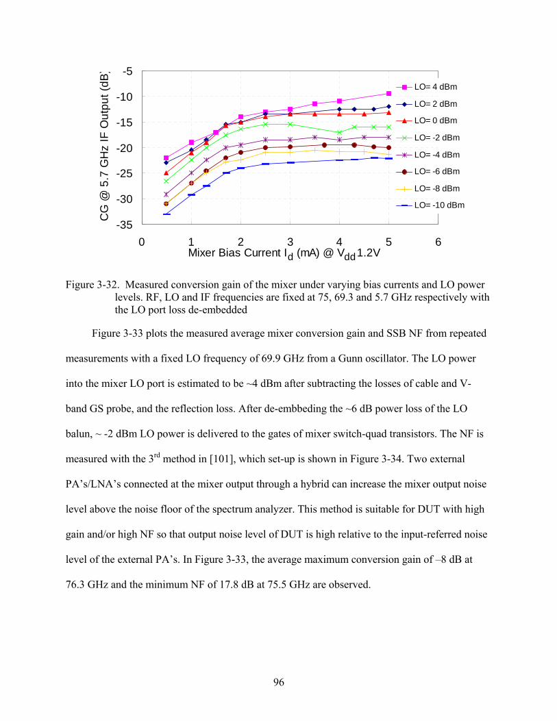
96
-35
-30
-25
-20
-15
-10
-5
0 1 2 3 4 5 6Mixer Bias Current I (mA) @ V 1.2V
CG
@ 5
.7 G
Hz
IF O
utp
ut
(dB
)
LO= 4 dBm
LO= 2 dBm
LO= 0 dBm
LO= -2 dBm
LO= -4 dBm
LO= -6 dBm
LO= -8 dBm
LO= -10 dBm
d dd
Figure 3-32. Measured conversion gain of the mixer under varying bias currents and LO power levels. RF, LO and IF frequencies are fixed at 75, 69.3 and 5.7 GHz respectively with the LO port loss de-embedded
Figure 3-33 plots the measured average mixer conversion gain and SSB NF from repeated
measurements with a fixed LO frequency of 69.9 GHz from a Gunn oscillator. The LO power
into the mixer LO port is estimated to be ~4 dBm after subtracting the losses of cable and V-
band GS probe, and the reflection loss. After de-embbeding the ~6 dB power loss of the LO
balun, ~ -2 dBm LO power is delivered to the gates of mixer switch-quad transistors. The NF is
measured with the 3rd method in [101], which set-up is shown in Figure 3-34. Two external
PA’s/LNA’s connected at the mixer output through a hybrid can increase the mixer output noise
level above the noise floor of the spectrum analyzer. This method is suitable for DUT with high
gain and/or high NF so that output noise level of DUT is high relative to the input-referred noise
level of the external PA’s. In Figure 3-33, the average maximum conversion gain of –8 dB at
76.3 GHz and the minimum NF of 17.8 dB at 75.5 GHz are observed.

97
-30
-25
-20
-15
-10
-5
73 74 75 76 77 78RF Frequency (GHz)
CG
(d
B)
10
15
20
25
30
35
NF
,NF
(d
B)
CGNFNF2
2
Figure 3-33. Measured average mixer conversion gain (CG), SSB NF and NF after de-embedding RF input balun loss (NF2) with a fixed 69.9-GHz LO provided by a Gunn oscillator. The LO power into the mixer LO port is ~4 dBm.
Figure 3-34. Measurement set-up for the 77-GHz mixer NF.
The down-conversion mixer exhibits conversion loss in both simulation and measurements
mainly due to the limited device power gain and inductor Q at mm-wave frequencies. A more
careful simulation of on-chip balun using HFSS shows two-port loss of ~6.5 dB instead of ~3 dB
as originally estimated with Fasthenry due to the mismatch at RF and LO ports. After de-
embedding the balun loss, the peak conversion gain of the mixer is ~ -1.5 dB and the NF at 75.5
GHz vary from ~10 dB to 13 dB from multiple measurements.

98
The mixer linearity is measured with the set-up plotted in Figure 3-35. The mixer has IP1dB
of -6.5 dBm at 76.3 GHz and IIP3 of 2.5 dBm (~-13 and ~-4 dBm after de-embedding the balun
loss) with two input tones at 76.3 and 76.31 GHz combined with a W-band magic-tee as shown
in Figure 3-36.
Figure 3-35. Measurement set-up for the 77-GHz mixer IIP3 (and IP1dB by using only one W-band signal source without the magic-tee).
-100
-80
-60
-40
-20
0
-30 -20 -10 0 10RF Input Power of 76.3 and 76.31 GHz (dBm)
IF O
utp
ut P
ow
er
(dB
m)
6.4 GHz IF Output6.39 GHz IF Output
IP - 6.5 dBm
IIP 2.5 dBm
1dB
3
Figure 3-36. Measured IIP3 with two input tones of 76.3 and 76.31 GHz and IP1dB with an input at 76.3 GHz under 1.2 V supply and 5 mA drain current. The power delivered into the LO port at 69.9 GHz is ~4 dBm. IIP3 of -4 dBm and IP1dB of -13 dBm are obtained after de-embedding the on-chip input balun loss.

99
Leakages (isolations) among ports are also measured from 58 to 78 GHz with the
measurement set-up similar to Figure 3-37. V-band GS/SG probes and cables, an OML V-band
harmonic mixer and an Agilent 8563E spectrum analyzer are used to detect the undesired
coupled signal power from one port to another. RF-IF, LO-IF, LO-RF and RF-LO isolations are
better than 38, 32, 21 and 31 dB respectively in the measured frequency range, as shown in
Figure 3-38.
Figure 3-37. Measurement set-up for the 77-GHz mixer LO-RF leakages.
-60
-50
-40
-30
-20
-10
55 60 65 70 75 80
RF/LO Frequency (GHz)
Leak
age
(dB
)
RF to IF Leakage
LO to IF Leakage
RF to LO Leakage
LO to RF Leakage
Figure 3-38. Measured leakages among mixer ports at VDD=1.2 V and 5 mA drain current. The power delivered into the LO port at 69.9 GHz is ~4 dBm for the RF/LO to IF leakage measurements.

100
Table 3-3 lists the performances of this mixer as well as those of other CMOS mm-wave
mixers from the literatures for comparison. Consuming only 6 mW, the highest average
conversion power gain of mixer is –1.5 dB at 76.3 GHz, the average NF is 11.3-13.5 dB between
76-77 GHz, and IIP3 and IP1dB are ~-4 and ~-13dBm after de-embedding the on-chip RF input
balun loss. Such performances are comparable to or better than other published CMOS mm-wave
down-conversion mixers at higher operating frequencies and lower LO power. This once again
suggests the feasibility of building a complete mm-wave transceiver on a single chip using low
leakage transistors in a 65-nm CMOS process for low-cost consumer-oriented applications.
Table 3-3. Performance comparisons of stand-alone CMOS mm-wave down-conversion mixer
CMOS Technol-ogy
RF/IF Freq. [GHz]
Topolo-gy
Conver-sion Gain [dB]
NF [dB]
IP1dB/ IIP3 [dBm]
LO-IF/ LO-RF Isolation [dB]
PDC [mW] @ Vdd [V]
LO Power [dBm]
Area [mm2]
130 nm, 85/135 GHz fT/fmax 8M [42]
60/ 2
Active balanced single-gate
-2 11.5 (sim)
-3.5/ N/A
10-14/ N/A
2.4 @ 1.2
0 2.72
90 nm, 150/200 GHz fT/fmax 5M [102]
62/ 2
Passive single-ended
-11.6 11.6 6/16.5 N/A 0 4 4
130 nm, 76/90 GHz fT/fmax 8M [103]
9-50/ 0.01
Active doubly balanced
>5 16.4 @15 GHz
N/A/ 4.5 @ 30 GHz
>20/ >40
97 @ 3.3
5 0.25
65 nm [104] 60/ 2
Passive singly balanced
-12.5 12.5 5/ N/A
>30 / N/A
0 8.7 0.47
130 nm, 85/90 GHz fT/fmax 8M [99]
35-65/ 3
Active doubly balanced SHM
-7.5 17.5 @40 GHz
-5 @ 60 GHz/ 9 @ 44 GHz
>50/ N/A
91 8 1
65 nm, low leakage NFET >150/ >110 GHz fT/fmax
6M (This work)
76/ 6
Active doubly balanced
-8 (-1.5 w/o balun loss)
17.8 (11.3 w/o balun loss)
-6.5 /2.5 (~-13/-4 w/o balun loss)
>32/ >21
6 @ 1.2
~4 on the LO port, ~ -2 on the mixer switch- gates w/o balun loss
0.42

101
3.5 Summary
In this chapter, several fundamental blocks in mm-wave receiver front-end implemented in
the TI 65-nm bulk CMOS process are presented. First, the design flow of an 80-GHz tuned
amplifier with six stages is given, followed by the discussion of non-ideal effects caused by on-
chip ground and supply network, and silicon substrate coupling. Measurements show the
amplifier achieves 12 dB gain at 79 GHz and NF less than 10.5 dB within the 6 GHz 3-dB
bandwidth. IP1dB of -21 dBm and IIP3 of -11 dBm are measured. Next, a compact 94-GHz LC-
type VCO with 5.8% tuning range is presented. Its output power reaches -5 dBm and the phase
noise is -106 dBc/Hz @10 MHz offset. Finally, a 76-77 GHz down-conversion mixer with
fundamental LO and 5 GHz IF is designed and implemented. Measurements show the highest
average conversion power gain of mixer is –1.5 dB at 76.3 GHz, the average noise figure is
11.3-13.5 dB between 76-77 GHz, and IIP3 and IP1dB are ~-4 and ~-13dBm after de-embedding
the on-chip RF input balun loss.
The simulated and measured results of mm-wave circuit blocks indicate the feasibility of
implementing an entire mm-wave receiver using low-leakage transistors of bulk CMOS, which
implies low-cost and high integration.

102
CHAPTER 4 APPLICATIONS FOR CMOS MILLIMETER-WAVE RECEIVER FRONT-END CIRCUITS
4.1 Introduction
The feasibility study for mm-wave receiver circuit blocks in Chapter 3 shows that it is
possible to build a complete mm-wave transceiver in the 65-nm low leakage bulk CMOS
process. Such transceiver can be used for many applications at mm-wave frequencies. Here, two
applications are considered. The first one is a mm-wave wireless interconnect system targeting to
alleviate some issues of conventional wire-based interconnect system, namely, complex I/O
wiring, larger package area and limited data bandwidth. This design is at system-level based on
circuit block performances in Chapter 3. The second application is a 77-GHz automobile radar
system. Receiver circuit design and experiments are the focus of that. In the following sections,
this application will be discussed. However, the system design details for mm-wave wireless
interconnects are given in Appendix A.
4.2 Introduction to 77-GHz Automobile Radar
Radar stands for radio detection and ranging. Radar systems are very useful in a multitude
of applications such as air defense systems, navigation, weather monitoring, and object detection
[105]. Simply put, all of these radar systems function on the same principle of radiating
electromagnetic energy away from an RF source and monitoring any reflected signals from
objects. The angle at which a receive antenna is pointed, the time delay between transmitted and
received signals, and any frequency variation between the transmitted and received signals,
together are used to determine the location, moving direction and speed of the detected object.
The received signal can also be analyzed to obtain the properties of the object such as the shape,
size, and constitutes. In recent years, radar-based driver assistance systems such as adaptive
cruise control (ACC) and collision avoidance have been introduced into the automobile market

103
to enhance the safety and comfort of driving. Most of these systems rely on microwave or mm-
wave radar to obtain the necessary information about the driving environment [106]. [107]. It is
estimated more than 10 radars per vehicle are needed for various needs, as shown in Figure 4-1.
Figure 4-1. Vehicle with multiple radar modules for various functions to make driving more safe and comfortable
Considering the sales of millions of units per year and the high probability of lowering life
and property losses on the road, it is not surprising that the automobile radar applications attract

104
strong interests from both the car and electronics manufacturers. Compared to the radar system at
lower frequency bands such as 5 GHz and 24 GHz, mm-wave system will need a smaller antenna
to obtain the needed directivity for higher angular resolution, thus making the radar more
compact and easier for installation in limited space available in a car, such as the space behind
the front bumper. Cost could also be lowered. On the other hand, higher frequencies in the EM
wave spectrum, such as infrared and optical wavelengths, would allow even narrower beam
width than at mm-wave frequencies for the same size of antenna. However, these shorter
wavelengths waves suffer from much larger attenuation during propagation especially from fog,
dust, smoke and others. 76-77 GHz in the mm-wave region is one frequency band designated for
automobile radar applications, which has relatively low excess propagation loss, as can be seen
in 1-2 of Chapter 1. More recently, a short-range wide band radar system (SRR) using 77-81
GHz is also proposed [107]. For simplicity, we will refer the automobile radar applications in
both bands as 77-GHz radar in the following sections.
Up to now, automobile radar circuits are mostly fabricated in III-V technology, which
contributes to the high cost and impedes the wide use. With the speed improvement of CMOS
technology, low-cost digital CMOS devices have been used to demonstrate circuits operating in
mm-wave band as discussed in Chapters 2 and 3. These suggest the possibility of highly
integrated automobile radar chips with much lower cost than those based on III-V technology,
even at frequency as high as 80 GHz.
To further study this opportunity, a 77-GHz pulsed radar transceiver architecture is
proposed in this chapter and the corresponding receiver front-end circuits are designed in the TI
65-nm CMOS technology. First, an overview for the proposed radar system is presented in the
next section.

105
4.3 Overview of the 77-GHz Radar System
For the proposed 77-GHz CMOS automobile radar system, it is assumed that a multi-beam
high gain antenna from Roadeye Ltd. [108] is used for both transmission and reception. The
front and rear view of antenna and its radiation pattern are shown in Figure 4-2. The three narrow
main beams in the center are for long range coverage and the two wider side beams are for wide
angle coverage. Transmitter and receiver circuits of the radar can be mounted behind the
Roadeye antenna, forming a compact radar module.
Figure 4-2. Multi-beam antenna and its radiation pattern for the proposed 77-GHz CMOS radar system.
To lower cost and to exploit the benefits of CMOS integration, transmitter and receiver
should be built on one die. Since 76-77 GHz is the operating range of the radar system,
transmitting and receiving in the only 1 GHz band at such high frequency and close distance
between a transmitter (TX) and a receiver (RX) will require impossibly high isolation among TX
and RX in a continuous wave radar as introduced in [109] to avoid serious mutual interference,
resulting from TX output signals being so much higher than the desired reflected signal the RX
needs to detect. Hence a pulsed radar architecture is chosen for the targeted radar system, which
transmits a 77-GHz wave modulated by a short square pulse, then turns off the transmitter and

106
turns on the receiver to listen for possible reflected signals. The time division transmitting and
receiving eliminates the mutual interference problem between TX and RX. The way pulsed radar
works is similar to a time-domain reflectometer many RF designers are familiar with.
In pulsed radar, the spatial resolution is determined by the time delay between the starting
moments of transmitter radiation and receiver sensing. Thus it is ultimately bounded by the
transmitted pulse width. To reduce the potential mutual interferences among multiple working
pulsed radars in a real driving environment, pseudo-random coded sequences of pulses can be
used to distinguish different vehicles.
Based on these, the proposed radar system specification is tabulated in Table 4-1. As seen
in Table 4-1, the pulsed radar targets a detection range of 1-150 m with pulse widths between 2.5
and 25 ns depending on the object distance from the radar, which translates to an RF signal
bandwidth of 800 and 80 MHz for a pulse-transmitting rate of 10 Hz. These narrow pulses allow
resolutions of 1 m for the range of 1-35 m and 3.75 m for 35-150 m. Also, pulse averaging and a
digital signal processing techniques can be used in the system to increase the detected signal
SNR (corresponding to detection error probability). The maximum number of integrated pulses
depends on the object distance.
Table 4-1. System specification for the proposed 77-GHz pulsed radar system Features Specifications
Range (m) 1-150
Resolution (m) 1-3.75
Pulse Width (ns) 2.5 – 25
Pulse Signal Bandwidth (MHz) 80 -800
Pout (dBm) 0 – 10
Averaging Pulse Number 10-5,000
Refresh Rate (Hz) 10
Receive Time Slot (S) 1.5

107
Assuming TX output power of 0-10 dBm, RX NF of 10 dB, minimum output SNR of 13
dB (corresponding to 10-8 detection error probability), link margin of 5 dB and detected object
radar cross section area of 1 m2, the radar equation [109] is used to calculate the detection range
Equation 4-1 for far and short range scenarios respectively. The results are summarized in Table
4-2 and 4-3.
sys
t
LSNRkTBF
nGPR
min3
22
max)4(
(4-1)
Table 4-2. Pulsed radar system range calculation for long distance detection Items Values Items Values
TX output power Pt 10 dBm B (bandwidth) 79 dB-Hz
Antenna gain (G) 25 dB (receive) + 30 dB (transmit)
Pulse width 25 nS
Radar cross section(s)
0 dB F (noise factor) 10 dB
@ 77-GHz -82.1 dB SNRmin 13 dB
n (number of integrated pulses)
37 dB Link margin (Lsys) 5 dB
KT -174 dBm/Hz Max. range Rmax 157 m
Resolution 3.75 m RX received power Pr @ Rmax
-104 dBm
Table 4-3. Pulsed radar system range calculation for short distance detection
Items Values Items Values
TX output power Pt 0 dBm B (bandwidth) 89 dB-Hz
Antenna gain (G) 25 dB (receive) + 30 dB (transmit)
Pulse width 2.5 nS
Radar cross section(s)
0 dB F (noise factor) 10 dB
@ 77-GHz -82.1 dB SNRmin 13 dB
n (number of integrated pulses)
10 dB Link Margin (Lsys) 5 dB
KT -174 dBm/Hz Max. range Rmax 11 m
Resolution 1 m RX received power Pr @ Rmax
-69 dBm

108
Notice that for narrower pulses (higher spatial resolution), the signal bandwidth is larger,
implying the background thermal noise power at the RX is higher and the maximum range will
be reduced.
4.4 Design and Measurement of an 80-GHz Down-Converter
Before a further study for the 77-GHz pulsed radar transceiver architecture and receiver
circuits, an 80-GHz down-converter aiming to demonstrate the feasibility of building a 77-GHz
receiver is designed and implemented using the low leakage transistors of TI 65-nm bulk CMOS
process.
The design of the 80-GHz down-converter is as follows: A higher peak gain and narrower
3-dB bandwidth design of the 80-GHz tuned amplifier with its performance shown in Section 3.2
(Figure 3-10 (A)) is cascaded with a 77-GHz pseudo-differential down-conversion mixer [110]
similar to the double-balanced mixer described in Section 3.4. Figure 4-3 illustrates that the
interface between the circuit blocks is changed from 50- matching to a series LC matching
network where L is provided by the parasitic inductance of the relatively long interconnect. The
balun at the RF port of 77-GHz mixer in Chapter 3 is removed because of its power loss (~ 3 dB)
at mm-wave frequencies. Hence, the mixer is modified from the differential input-differential
output topology to a single-ended input-differential output topology (pseudo-differential) as
shown in Figure 4-4. Tables 4-4 and 4-5 list the component values in Figure 4-3 and Figure 4-4,
respectively.

109
Figure 4-3. Schematic of the tuned amplifier in the 80-GHz down-converter.
Figure 4-4. Schematic of the pseudo differential mixer in the 80-GHz down-converter.

110
Table 4-4. Component values of the tuned amplifier in the 80-GHz down-converter
M1-M6 (W) (m) Pad Cap. (fF) Cbypass (pF) C1 (fF)
18 80 1 190
Lg1 (pH) Ls1 (pH) Ld1 (pH) C2 (fF)
190 20 100 130
Lg2 (pH) Ls2 (pH) Ld2 (pH) C3 (fF)
110 15 90 130
Lg3 (pH) Ls3 (pH) Ld3 (pH) C4 (fF)
110 10 100 130
Lg4 (pH) Ls4 (pH) Ld4 (pH) C5 (fF)
110 10 80 130
Lg5 (pH) Ls5 (pH) Ld5 (pH) C6 (fF)
110 5 80 120
Lg6 (pH) Ls6 (pH) Ld6 (pH)
110 5 110
Table 4-5. Component values of the pseudo differential mixer in the 80-GHz down-converter
M7-M12 (W) (m) Lg_mix (pH) Cg_mix (pF) Ls_mix1,2 (pH)
32 80 1 10
Ltail (pH) Lm1,2 (pH) Lp1,2 (pH) Ct1 (fF)
200 100 120 80
Ct2 (fF) Cdif_mix1,2 (fF) Ldif_mix1,2 (pH) Cbypass_mix(pF)
140 200 360 24
Transistors M7-M12 are 32 m wide. The highest mixer conversion gain is achieved with
600 mV p-p LO swing on the gates of M9-M12. An 1:1 on-chip balun built with two overlapping
single loops in metal6 and pad aluminum layer is used at the LO port of the mixer to convert
external single-ended LO signals to differential LO signals, similar to that in [100]. The balun
has ~3 dB loss in HFSS simulations at 60 GHz. Metal capacitors (Ct1-Ct4) are used to tune the
balun to ~60 GHz. Series inductors Lp1 and Lp2 boost the LO swing at the gates of NMOS

111
switching transistors (M9-M12), compensating part of the LO power loss from the balun and
relaxing the external V-band LO signal drive requirement.
M7 and M8 work as an active balun. The tail inductor, Ltail forms a resonant tank with the
source degeneration inductors (LS_mix1 and LS_mix2) and parasitic capacitances of M7 and M8. The
tail inductor increases the common mode rejection of mixer. The inductors make the input
impedance seen at the gate of M7 higher and its gate to source voltage gain closer to the
theoretical value of ½ for increased single-ended to differential conversion gain. The simulated
amplitude imbalance between the two IF outputs is ~1.5 dB and can be compensated in
differential circuits following the mixer. Lm1 and Lm2 are inserted between M7, M8 and the
switch-quad to boost the mixer conversion gain by ~2 dB [100]. In the mixer layout, the
symmetry of signal paths is critical to lower the leakage among ports.
In simulations, the mixer shows a peak conversion gain of –3.5 dB at 79.5 GHz and 11-dB
minimum NF. For the whole down-converter, the simulated conversion gain and NF at
VDD=1.2V are 19 dB and 7.7 dB at 80 GHz with 600-mV p-p LO on the gates of NMOS
switching transistors.
A die photo of the down converter is shown in Figure 4-5. The down-converter area is
1.07X0.55 mm2 including bond pads. Figures 4-5 (A), (B) and (C) are the photographs of down-
converter, and zoom-ins for the tuned amplifier and mixer, respectively. As can be seen, line
inductors are used on the drains and sources of transistors in the tuned amplifier because of their
higher Q factor, while spiral inductors with custom dummy metal fills are used in other places
for more compact layout. The on-chip metal1-6 stacked ground plane and dense dummy metal
fills added by the foundry can also be seen in Figure 4-5.

112
A
B
Figure 4-5. The 80-GHz down-converter die photo A) The whole down-converter. B) Close-up of the tuned amplifier circuit. C) Close-up of the mixer circuit.

113
C
Figure 4-5. Continued
With measurement set-ups similar to that have been described in Chapter 3 for mixer
measurements, the down-converter is characterized on chip with a W-band GSG probe, a V-band
GS probe and a 40-GHz GSSG probe with an external hybrid connected at the IF port. The
matching characteristics at RF, LO and IF ports are measured with an Agilent PNA E8361A and
two N5260A frequency extension modules. The measurements and simulations of frequency
tuning for RF, LO and IF port matching are close, but the actual matching is not as good as the
simulated, as shown in Figure 4-6. This is likely due to underestimation of signal pad losses
through EM fields coupling to dummy fill structures underneath and around the pads, which
lowers the Q of pads and hence the matching networks, since pads are an integral part of the
matching networks. Such effects are verified with simulations. The measured |S11|, |S22| and |S33|
around 80, 60 and 20 GHz respectively are less than –8 dB.

114
-16
-12
-8
-4
0
4
0 20 40 60 80 100
Frequency (GHz)
|S11
|, |S
22| a
nd |S
33| (
dB) |S | @RF Port
|S | @LO Port|S | @IF PortSim. |S | @RF PortSim. |S | @LO PortSim. |S | @IF Port
11
22
33
11
22
33
Figure 4-6. Measured and simulated impedance matching of the down-converter.
The conversion gain of down-converter is characterized with an Agilent E4448A spectrum
analyzer at VDD=1.2 V and 1.5 V. Figure 4-7 shows the measured conversion gain and SSB NF
of the down-converter with 60-GHz LO signal generated by an N5260A extension module
cascaded with two Terabeam V-band power amplifiers. The power delivered to the LO port
measured with an OML V-band harmonic mixer and a spectrum analyzer is ~4 dBm. It is
estimated that ~1 dBm LO power is available at the output of on-chip balun. As can be seen, the
down-converter achieves maximum conversion gain of 16 dB and minimum NF of 9 dB at 80
GHz and VDD=1.2 V. The 3-dB bandwidth is ~5 GHz around 80 GHz. At 1.5 V and 63-mW
power consumption, the maximum conversion gain of 18 dB and minimum NF of 8.4 dB are
achieved. The measured peak conversion gain and lowest NF at 1.2 V supply and 53 mW power
consumption are 3 dB lower and 1.3 dB higher, respectively than the simulated results including
the non-ideal ground effects. The difference may be attributed to the component model
inaccuracy, e.g., the transistor model parameters being used are intended for low GHz
applications. Figure 4-8 plots the conversion gain at varying LO power levels. The peak

115
conversion gain increases from ~ 12 dB to ~16 dB when the power available to the LO port of
down-converter is increased from -2 dBm to 4 dBm (-5 dBm to 1 dBm after de-embedding the
on-chip balun loss of ~ 3 dB).
0
5
10
15
20
25
30
75 77 79 81 83 85RF Frequency (GHz)
Con
v. G
ain
(dB
)
7
9.5
12
14.5
17
19.5
22
NF
(dB
)
Conv.Gain @1.2V
Conv.Gain @1.5V
Sim.Conv.Gain @1.2V
NF @1.2 V
NF @1.5 V
Sim.NF @1.2V
Figure 4-7. Measured conversion gain and NF of the down-converter for fixed LO frequency of 60 GHz.
-4
0
4
8
12
16
75 77 79 81 83 85
RF Frequency (GHz)
Con
v. G
ain
(dB
)
Conv.Gain@ 4 dBm LO
Conv.Gain@ 1 dBm LO
Conv.Gain@ -2 dBm LO
Conv.Gain@ -5 dBm LO
Figure 4-8. Measured conversion gain of the down-converter at varying power levels of the 60-GHz LO delivered to the LO port.

116
For IIP3 measurement, two test tones at 81 and 81.01 GHz are gernerated using two
N5260A extension modules and combined with a DualComm W-band magic-tee. A DualComm
Gunn oscillator delivers ~4 dBm LO power at 61 GHz to the LO port of the circuit after de-
embedding the loss of V-band cables, probe and circuit return loss. Figure 4-9 shows the
measured IIP3 and IP1dB of the down-converter are -16 dBm and -26 dBm at VDD=1.2V. LO-RF
(input of tuned amplifier) and LO-IF leakages are measured to be less than -61 and -24 dB,
respectively (Figure 4-10).
-95
-75
-55
-35
-15
5
-50 -40 -30 -20 -10
RF Input Power of 81 and 81.01 GHz (dBm)
IF O
utpu
t Pow
er (
dBm
)
20.01 GHz IF Output20.02 GHz IF Output
IP1dB -26 dBm
IIP3 -16 dBm
Figure 4-9. Measured IIP3 and IP1dB of the down-converter at 81 GHz.
-95
-80
-65
-50
-35
-20
45 50 55 60 65 70 75
LO Frequency (GHz)
Leak
age
(dB
)
LO-->IF
LO-->RF
Figure 4-10. Measured LO-RF and LO-IF leakages of the down-converter.

117
Table 4-6. Comparisons of W-band CMOS receivers
W-Band Receivers
[74] [75] [76] This Work
CMOS technology
90-nm, fmax>120 GHz
65-nm, low Vth
fmax/fT 240/165 GHz @ Vds 0.7 V, 7M
65-nm, low Vth, fmax/fT 280/195 GHz @ Vds 1.2 V, 7M
65-nm, high Vth (>0.6 V), fmax/fT >110/>150 GHz, 6M (Dummy metal fills enforced on all passives)
RF/IF freq. [GHz]
57-77/0-2 75-91/0-10 76-95/0-18 77-82/17-22
Integration
RX (LNA+RF Mix. + IF Mix. + IF Amp.) + PLL
RX (LNA+ Mix. + IF Amp.)
RX (LNA+Mix. +IF Amp) +VCO +Div2
RX (LNA+Mix.)
Conversion gain [dB]
19 @ 77 GHz (voltage gain)
13 @ 80 GHz 7.5 (1.2 V)/ 2
(1.5 V) @ 85 GHz
16 (1.2 V)/18 (1.5 V) @ 80 GHz
NF [dB] N/A 8.5-10 (DSB) 7-10 (1.2 V)/6-9
(1.5 V) DSB) 9-11(1.2V)/8.4-10.5
(1.5V) (SSB)
IP1dB/ IIP3 [dBm]
-16/ N/A -16/ N/A -18/ N/A -26/-16
LO-IF/LO-RF leakage [dB]
N/A N/A /< -60 N/A <-23/<-60
LO power [dBm]
N/A 5 N/A 4 (1 dBm after de-
embedding on-chip balun loss)
PDC [mW] @ Vdd
60(RX)+72(PLL) @1.5 V
89 @1.5 V
78(RX) @1.5 V + 128 (VCO+Div2) @ 1.2 V
53 @1.2 V 63 @1.5 V
Area [mm2] 1.0x1.0 0.46x0.5 1.09x0.6 1.07x0.55
Table 4-6 summarizes the performance of this down-converter as well as those of other
published CMOS W-band receiver front-end for comparison. It shows that at lower DC supply
voltage, the down-converter in this paper fabricated using low-leakage (high Vth) transistors of a
lower cost 65-nm CMOS process with a fewer number of metal layers achieves a higher
conversion gain and better SSB NF than the two RX’s fabricated using low Vth general purpose

118
transistors in 65-nm CMOS [75], [76]. These are attributed to the use of a 6-stage tuned
amplifier, elimination of lossy balun in the RF signal path, optimization of both active and
passive components, especially the latter in the presence of dummy metal fills, and optimization
of the bandwidth for the radar application. Due to the high Vth of the transistors and relatively
high gain of the tuned amplifier, the linearity of the down-converter is lower than the RX’s in
[75], [76]. Overall, the down-converter achieves comparable performance as those fabricated
using the general purpose (low Vth) NMOS transistors of a 65-nm CMOS technology.
With the successful demonstration of the 80-GHz down-converter, we will continue to
investigate the feasibility of a more complete integration of mm-wave receiver front-end for 77-
GHz band radar application in the low-cost 65-nm CMOS technology.
4.5 Radio Architecture for the 77-GHz Pulsed Radar System
For the proposed 77-GHz pulsed radar system, high performance/cost ratio is the key to the
success in the high volume market. Integrating as many necessary circuit blocks in a single
CMOS chip should lower external component counts and packaging cost. With this goal in mind,
two basic architectures of RF transceivers, direct conversion and dual conversion are evaluated.
/2/128
51 GHz
51 GHz
25.5 GHz76.5 GHz On-chip Dipole Antenna
25.5 GHz
76.5 GHz PA
PFD
LF
RX BBOutput
TX BB Input Modulating PA
fREF
76.5 GHzOffset
Mixer
76.5 GHz LNA
25.5 GHz Tuned Amp
77-GHz Radar RF SOC in CMOS
AC Coupling Cap
/2/128
51 GHz
51 GHz
25.5 GHz76.5 GHz On-chip Dipole Antenna
25.5 GHz
76.5 GHz PA
PFD
LF
RX BBOutput
TX BB Input Modulating PA
fREF
76.5 GHzOffset
Mixer
76.5 GHz LNA
25.5 GHz Tuned Amp
77-GHz Radar RF SOC in CMOS
AC Coupling Cap
Figure 4-11. Simplified block diagram of the CMOS heterodyne radar transceiver.

119
A dual conversion heterodyne architecture utilizing a single PLL (Figure 4-11) is proposed
to alleviate several issues with the direct conversion architecture. The proposed architecture can
effectively eliminate the problems of VCO being pulled by the pulse modulated 76.5-GHz carrier
from the transmitter and the LO leakage to the receiver which can swamp out the wanted
received signal, as well as relaxing the maximum operating frequency requirement of PLL to 51
GHz, which can not only improve the tuning range and phase noise performance of the
synthesizer but also allow the use of compact and wide-locking range static dividers. For the dual
conversion architecture, potentially, there are more flexibility for the trade-off of individual
circuit block performance in the RX chain to meet the overall system requirements. This is an
important advantage due to the limited performances of CMOS mm-wave circuit blocks.
The 51-GHz PLL output can be divided by two to generate the 25.5-GHz signal as the LO
for the second frequency down-conversion in the RX. Also, the 51 and 25.5 GHz signal can be
offset-mixed to generate the 76.5 GHz carrier needed in the TX. The lower sideband resulting
from the offset mixing is 51 GHz below the wanted carrier and can be easily filtered out.
25.5 GHzLO
76.5 GHz RX Input
RX BBOutput
76.5 GHz LNA
25.5 GHz Tuned Amp
51 GHzLO
AC Coupling Cap
76.5 GHz Mixer
25.5 GHz Mixer
1
2
3
25.5 GHzLO Buffer
51 GHzLO Buffer
25.5 GHzLO
76.5 GHz RX Input
RX BBOutput
76.5 GHz LNA
25.5 GHz Tuned Amp
51 GHzLO
AC Coupling Cap
76.5 GHz Mixer
25.5 GHz Mixer
1
2
3
25.5 GHzLO Buffer
51 GHzLO Buffer
Figure 4-12. RX block diagram showing the main 25.5-GHz LO leakage paths
In the frequency plan, the received 76.5-GHz signal has image frequency at ~25.5-GHz.
Due to the high IF of 25.5-GHz for this dual conversion architecture, the received image
interference can be effectively attenuated by the band-pass filtering effect of the mm-wave LNA

120
and mixer. However, at the input of the 25.5-GHz down-conversion mixer, there is not only the
desired down-converted 25.5-GHz signal but also leakages of the 25.5-GHz LO. The 25.5-GHz
LO can take several main paths to end up at the input of the 25.5-GHz mixer (Figure 4-12): (1)
Leak to the 25.5-GHz mixer RF input due to its limited LO-RF isolation. (2) Leak to the input of
the 25.5-GHz tuned amplifier. (3) Leak to the input of the 76.5 GHz mixer, and mix with the 51-
GHz LO to generate the 25.5 GHz signal. These leakages may be from the EM near-field
coupling and EM wave radiation through the signal paths of circuits, conductive silicon substrate
and non-ideal on-chip power and ground lines. For several of these cases, the problem is
compounded by the subsequent amplification of the IF amplifier. This is a serious concern that
must be addressed during the design of the receiver circuit.
Notice that in our actual circuit design in the following three sections, all the circuit blocks
are intentionally designed to operate at ~10% higher frequencies than those shown in Figure 4-11
to provide an adequate margin for frequency tuning down due to variations and underestimated
parasitic capacitances.
FRONT VIEW TOP VIEW
FRONT VIEW
AN
TE
NN
A L
EN
GT
H
50 LUMPED PORT
AIR BOX
RECTANGULARWAVEGUIDE
TO HIGH GAIN ANTENNA
METAL PLANE BENEATHTHE SUBSTRATE
PCB SUBSTRATE
SILICON SUBSTRATE
ANT WIDTH
50 WAVEPORT
BIRD’S EYE VIEW
FRONT VIEW TOP VIEW
FRONT VIEW
AN
TE
NN
A L
EN
GT
H
50 LUMPED PORT
AIR BOX
RECTANGULARWAVEGUIDE
TO HIGH GAIN ANTENNA
METAL PLANE BENEATHTHE SUBSTRATE
PCB SUBSTRATE
SILICON SUBSTRATE
ANT WIDTH
50 WAVEPORT
BIRD’S EYE VIEW
Figure 4-13. Three-dimension modeling of the transition from the 76.5-GHz on-chip dipole feed to the waveguide section of a high gain antenna

121
As discussed, it is expected that a T/R switch in the TI 65-nm process at 77-GHz will have
an insertion loss 4-5 dB based on the measured insertion loss of ~4.5 dB at 67 GHz. This
insertion loss is fundamentally limited by the relatively large losses in passive components such
as inductors and capacitors, and PN junctions of drain and source of transistors in the low-cost
digital process. This degrades the TX output power and RX sensitivity, limiting the link margin
of the system. To avoid the switch loss, in the radio architecture proposed in Figure 4-11,
separate on-chip feeds (dipoles) for waveguides at 76.5 GHz are integrated for TX/RX. As
shown in Figure 4-13, the TX feed transmits signal to and the RX feed receives signal from a
waveguide of the high gain Roadeye antenna [108] in Figure 4-2. For this approach, there is no
need for mm-wave off-chip connections through a package and a substrate. This eases the
assembly of the radar module and lowers the cost. Studies of this on-chip feed (dipole) to
waveguide transition have been conducted and EM simulations show ~3.5 dB loss for the dipole
feed-to-waveguide transition around 77-GHz. This loss is expected to be ~0.5 dB different from
that of a system using the best mm-wave T/R switch and off-chip waveguide feeds connected
through bond wires-transmission lines [111].
4.6 Design of Receiver Chain for the 77-GHz Pulsed Radar Transceiver
The 77-GHz radar receiver chain is designed in the TI 65-nm CMOS process, which
includes a 82.5-GHz RF tuned amplifier and an active down-conversion mixer (Figure 4-14)
followed by a 27.5-GHz IF tuned amplifier and a passive down-conversion mixer, and finally
baseband HPF and current buffer (Figure 4-15).
A differential (pseudo-differential) topology is desirable for its rejection of common mode
noise and non-ideal ground/supply effects as discussed in Chapter 3. This feature is especially
important in the noisy on-chip environment where circuit blocks can interfere with each other
through undesired coupling. Besides, the on-chip dipole feed can be conveniently connected with

122
the first differential amplifier stage of the receiver front-end and there is no need for single-
ended to differential conversion. However, since only single-ended (SE) probes are available at
77-GHz, for the first RF amplifier, it is designed as three SE CS amplifier stages cascading with
Figure 4-14. Receiver mm-wave front-end schematic (RF stages) of the 77-GHz radar system
three differential CS amplifier stages with the SE to differential conversion accomplished by a
77GHz line balun discussed in Chapter 2. The primary winding of the line balun serves as an
inductive load for the third stage SE CS amplifier. The first three stages of SE CS amplifiers
facilitate SE GSG probe testing and suppress the RX NF degradation from the line balun loss.
The SE CS amplifiers can be changed to differential CS amplifiers and the line balun can be
removed if the receiver chain is integrated with an on-chip dipole feed.
All the CS amplifier design follows the method discussed in Chapter 3. The common-
mode rejection ratio (CMRR) of the 3 differential CS amplifier stages are enhanced by inserting
inductors between the common source of CS amplifier and on-chip ground. In simulations, the
RF amplifier achieves a differential voltage gain of ~14 dB and good input match is obtained
between 77 and 85 GHz. The CMRR is simulated to be ~40 dB and reverse gain is ~ -50 dB. The

123
amplitude imbalance between the two differential output is less than 0.5 dB and the phase error
is less than 10 degree.
Figure 4-15. Receiver IF and BB stages schematic of the 77-GHz radar system
The RF down-conversion mixer is a double-balanced Gilbert cell and its design is similar
to the 77-GHz down-conversion mixer core design in Chapter 3. The LO frequency for the mixer
is ~55 GHz. There is no need for an on-chip balun at the RF input of the mixer since the
amplifier preceding it already provides differential signals, but the LO input of the mixer still
requires an on-chip balun if the receiver is tested with an external LO. Notice that the mixer
switch quad transistor sizes should not be excessively large so that he drive requirement of mm-
wave LO can be lowered. In simulations, this mixer obtains a voltage conversion gain of ~ -2.5
dB, LO-RF isolation of ~20 dB and CMRR of ~20 dB. The RF amplifier and mixer combination
shows NF of ~ 8.7 dB in simulations.
The IF amplifier is a cascade of 4 stages of differential cascode amplifiers, which should
increase the reverse isolation at 26 GHz. The transistor sizes are selected for high gain and low
NF. The whole IF amplifier can provide ~20 dB voltage gain and its CMRR is more than 60 dB.

124
The block following the IF amplifier is an IF mixer, which down-converts the incoming
signal centering at ~27 GHz to baseband. A double-balanced passive mixer topology is chosen
for the IF mixer. By trading off conversion gain, the relatively high linearity and low flicker
noise of the passive mixer compared to active mixer help maintain the output signal quality at
baseband. In simulations, the 26 GHz passive mixer achieves voltage conversion gain of ~-6 dB
The baseband differential signal output from the passive mixer will then enter a simple
HPF consisting of a series metal coupling capacitor and a resistor shunt to ground, and then to a
current source follower that acts as a signal buffer to an external load. The HPF 3-dB bandwidth
is set to ~1 MHz to filter out any other DC offset and low frequency noise present. The desired
received signal will only lose a very small portion of its energy through the HPF because the
signal is supposed to occupy at least 40 MHz baseband bandwidth (for pulse width of 25-ns)
according to the pulsed radar system design in Section 4.3.
The coupling cap and shunt resistor values are co-optimized with the current source
follower to obtain the best signal gain from the passive mixer to the off-chip 50- load
emulating the input resistance of test equipment. The transistor sizes of current source follower
are selected for a good compromise between large driving current and small loading to the
passive mixer. In simulations, the combination of baseband HPF and current source buffer
driving 50 ohm load shows ~ -10 dB voltage gain and bandpass characteristics between ~1MHz
and 3 GHz.
For the entire receiver chain, the conversion gain is ~15 dB and the NF is ~ 10.5 dB in
simulations, assuming the 55 and 27.5 GHz LO signal swings are both 600 mV peak-to-peak.
With the preliminary RX chain circuit designs and simulations in place, we are ready to
look back at the 27.5 GHz LO leakage problem discussed in the previous section. The amplitude

125
Table 4-7. Estimation of 27.5-GHz local oscillation leakage at the input of 27.5-GHz down-conversion mixer
Simulated circuit block Forward gain/ conversion gain (dB)
Reverse loss/LO-RF isolation (dB)
82.5-GHz LNA -50 @27.5 GHz 100 @27.5 GHz
82.5-GHz down-conversion mixer (Mixer 1)
-26 @27.5 GHz (CMRR 20 dB)
100 @27.5 GHz
27.5-GHz tuned amplifier (Tuned Amp)
21 @27.5 GHz (CMRR 50 dB) 40 @ 27.5 GHz
27.5-GHz down-conversion mixer (Mixer 2)
-6 @ 27.5 GHz (IV1dB ~0.8 V) 30 @27.5 GHz
Estimated coupling loss (dB) 24 (from 27.5 GHz LO buffer output to the 27.5-GHz tuned amplifier input)
30 (from 27.5 GHz LO buffer output to the 76.5-GHz mixer input)
Simulated 27.5-GHz LO buffer output amplitude
0 dBV (1 V)
27.5-GHz LO leakage of Path 1LO buffer output Mixer 2 LO port Mixer 2 input
0-30 = -30 dBV
27.5-GHz LO leakage of Path 2LO buffer outputTuned Amp inputMixer 2 input
0-24-20+21 = -23 dBV Assume 1/10th of the coupled voltage are differential signal
27.5-GHz LO leakage of Path 3: LO buffer output Mixer 1 inputTuned Amp inputMixer 2 input
0-30-6-26+21= -47 dBV Assume 1/10th of the coupled voltage are differential signal
27.5-GHz LO total leakage of Path 1,2 & 3
Amplitude 0.07 V < 0.8 V (IV1dB of Mixer 2)
of total 27.5-GHz LO leakage at the input of 27.5-GHz mixer can be roughly estimated to be ~ -
23 dBV (0.07 V) based on the simulated circuit performances and estimated coupling losses
from the past measurements on circuits fabricated in the 65-nm process (Table 4-7). The 27.5-

126
GHz mixer has a simulated IV1dB of ~0.8 V and the leaked 27.5-GHz signal at the input of the
mixer will be down-converted to become DC offset/low frequency noise with a bandwidth of ~1-
MHz at the output of the mixer, which is easily removed by the RC HPF at the baseband. So this
leakage should not cause nonlinear distortion to the down-conversion process.
This analysis shows that the 27.5-GHz LO leakage should not affect the operation of RX
chain, and the frequency plan introduced in the previous section should work. However,
measurements will ultimately determine the viability of the frequency plan. A new frequency
plan may be needed in case the original plan is found to degrade the RX performance. E.g., a 60-
GHz LO and its divided-by-4 product (15 GHz) could be used to realize the radar RX and
mitigate the LO leakage and image problems.
4.7 Design of Frequency Generation System for the 77-GHz Pulsed Radar Transceiver
In the 77-GHz radar transceiver architecture discussed above, a mm-wave frequency
generation system (synthesizer) is a vital circuit block providing high frequency LO signals for
Figure 4-16. Block diagram of the 51-GHz PLL frequency synthesizer (in dash box) in the proposed 77-GHz radar transceiver

127
both generating pulses of carrier around 76.5 GHz in the pseudo direct conversion TX and
down-converting the received pulses to baseband in the dual conversion RX. As shown in Figure
4-16, the frequency synthesizer consists of a 51-GHz PLL, multiple buffers tuned at different
frequencies and an up-conversion offset mixer.
At the core of synthesizer, the 51-GHz PLL is a 4th-order loop with a charge pump, where
the RC loop filter bandwidth is set to ~250 kHz and the reference frequency is ~225 MHz. With
this arrangement, the severe reference spurs shown in mm-wave PLL such as the one in [112]
hopefully can be attenuated to more than 40 dBc. Only divide-by-2 frequency dividers [113] are
needed in the PLL, which mitigates the complexity of mm-wave PLL design. As mentioned in
Section 4.5, all circuit blocks are intentionally designed at ~10% higher frequencies than those
shown in Figure 4-16 to provide a margin for frequency tuning down due to variations and
underestimated parasitic capacitances.
In the loop, a 55-GHz VCO with a cross-coupled NMOS pair similar to the 94-GHz VCO
discussed in Chapter 3 is utilized. In simulations, the VCO is tuned from 55 to 61 GHz to cover
the possible frequency shifting caused by process and temperature variations. The operating
frequencies of all other components for the synthesizer are tuned higher accordingly in
simulations.
A chain of asynchronous divide-by-2 static frequency dividers provides a division ratio of
256. A 2-stage tapered buffer (Buffer 1) isolates the VCO core from the 1st frequency divider,
and Buffers 2 and 3 for driving the LO port of the 1st mixer in the RX chain and the RF port of
the up-conversion offset mixer. ~2-m wide differential top metal lines compromising parasitic
resistance and capacitance at ~60 GHz are used to distribute the VCO buffer output signal to the

128
three circuit blocks. The parasitic inductances of these interconnects are exploited to form series
peaking networks to mitigate signal attenuation.
The first divide-by-2 circuit plays a critical role in determining the maximum operating
frequency of the PLL, and it is the most challenging design among the dividers. An injection-
locked frequency divider (ILFD) can be used as the first divider as in [112]. ILFD can operate at
very high frequencies, but its locking range usually is narrow and hence its robustness over
process and temperature variations is a concern. From this point of view, the current mode logic
(CML) type static dividers with a wider locking bandwidth and greater tolerance to the variations
are preferred. With the scaling of CMOS technology into nano-scale, MOS transistors are
becoming faster and it should be possible to use a CML type static divider instead of the ILFD as
the first divider stage for the 51-GHz PLL [112]. With the TI 65-nm CMOS process low leakage
transistors, a latch-biased static divider modified from [114] for low voltage operation, as shown
in Figure 4-17, is designed and optimized to achieve the necessary locking frequency.
A
Figure 4-17. Latch-biased static frequency divider used for the 1st and 2nd stage of divider. A) The schematic. B) The 1st divider layout with custom metal6 dummy fills and dummy blocks to reduce the parasitic capacitive load for the divider.

129
B
Figure 4-17. Continued
For this latch-biased divider, the gate of the latch tail current source transistor is connected
to a constant bias instead of the input high frequency clock signal. In this way, the divider
capacitive load to the previous stage is reduced. The biased latch also provides regenerative gain
for the divided-down signal without the need for waiting to be switched on by the mm-wave
clock signal. This decreases the signal transition times and enhances the divider speed. A small
sized PMOS transistor is used as a resistive load in the divider because of the relatively large
polysilicon resistor variation in the TI process. Also, the parasitic capacitive load added by the
PMOS load in the TI 65-nm CMOS is smaller and the impact on the maximum locking
frequency is small in simulations.
Due to the short distances between the back-end metal layers and substrate, and the dense
metal dummy fills in the TI process, the parasitic capacitances from the wiring within the divider
and between divider blocks, and the floating metal dummy fills above the divider are non-
negligible portion of the total capacitive load of divider. For a divider working at high
frequencies, these parasitics should be considered in the divider design. Besides, since such
parasitics from wirings and dummy fills do not scale with divider transistor sizes in the first

130
order, to maintain a certain swing at the divider output and to minimize the RC delay in the
positive feedback loop of these flip-flop style static dividers, the transistors need to be sized-up
to drive more current into the load. This must be balanced by the fact that the larger the transistor
size in the first divider, smaller the input swing set by the preceding VCO buffer.
In the implementation, custom metal6 (M6) dummy fills and dummy blocks are juxtaposed
with the power supply lines and bypass capacitors (Figure 4-17(B)) to satisfy the metal density
rules. This reduces the parasitic loading of divider by ~8 fF and increases the maximum dividing
frequency by ~10%, as shown by the simulated input sensitivity curves in Figure 4-18. A 2-stage
tapered buffer (Buffer 4) is inserted between the first two dividers to increase the 1st divider
output swing for driving the 2nd divider, and Buffers 5 and 6, hence improving the robustness of
divider chain.
The 2nd divider in the divider chain probably is as important as the first one for setting the
maximum operating frequencies. The input transistors of the 2nd divider contributes a large
portion of the capacitive load to the first divider, which then limits the transistor sizing of the 2nd
divider. Since the 2nd divider actually works at quite high frequency (~27-30 GHz). Its transistor
sizes cannot be too small. Since each divider presents loading to the previous stage, and the
cascading of these dividers (DC coupled) changes the bias points of individual divider, it is
necessary to co-optimize the VCO and the divider chain as a whole to make sure the divider
chain works properly.
In simulations, the first stage latch-biased divider achieves a locking range between 52 and
71 GHz for a sinusoidal clock input with 600 mV peak-to-peak swing and the whole divider
chain can successfully divide the VCO output within the tuning range.

131
-6
-5
-4
-3
-2
-1
0
1
40 50 60 70 80
Input Frequency (GHz)
Inp
ut
Po
we
r (d
Bm
)
w/ Custom Dummy Block
w/o Custom Dummy Block
Figure 4-18. Simulated input sensitivity plot of the 1st latch-biased static frequency divider.
Following the divider chain, a dead-zone free, three-state phase-frequency detector (PFD)
and charge-pump (CP) use the same topology as that in [115] and [116]. The transistor sizes of
charge-pump PMOS/NMOS output current sources are optimized to obtain charge/discharge
current matching to reduce the reference spurs in simulations. A 3rd order RC loop filter [115] is
used to set the loop bandwidth to ~250 kHz. This along with the relatively high reference
frequency of ~225 MHz further attenuates the reference spurs.
All the tapered buffers (Buffers 1-7) use the balanced common source tuned amplifier
topology for improved operation at low voltage. Their LC resonant tank loads use spiral
inductors optimized with custom dummy metal fills and dummy blocks as discussed in Chapter
2. This reduces the chip area and makes the necessary connections easier. Notice that the 3-dB
gain bandwidth of these buffers should not be too narrow. Otherwise, if the buffers are mistuned,

132
they may adversely affect the whole synthesizer operation. Just like the divider chain, the multi-
stage buffer should be optimized as a whole once the transistor size and inductor load values are
roughly decided. Finally, as in the design of amplifier, the stability of these buffers should be
maintained.
A double balanced Gilbert cell topology, which is the same as the core circuit of the down-
conversion mixer discussed in Chapter 3, is used in the offset mixer for up-converting the ~55
GHz output from VCO to ~83 GHz. It is designed to maximize the conversion gain for an RF
input of 55 GHz and LO input of 27.5 GHz coming from the VCO output buffer and the first
stage divider output buffer, respectively. The simulated mixer conversion gain is ~–10 dB at ~83
GHz assuming a 600 mV p-p LO signal at ~27-GHz. This LO signal is from the 1st frequency
divider output, which can be more easily amplified compared to the ~55-GHz signal. A 4-stage
tapered buffer (Buffer 7) following the offset mixer provides the input to the PA in TX. It
amplifies the desired ~83-GHz signal by ~8 dB and attenuates the ~27-GHz image and ~55-GHz
leakage by more than 30 dB. For single-ended measurement, one side of the Buffer 7 outputs is
terminated by an on-chip 50- resistor. The whole up-conversion mixer chain including all the
related buffers consumes ~60 mW in simulations.
The frequency synthesizer and receiver chain of the radar discussed above should be
integrated to form a complete mm-wave radar receiver front-end. The desired LO signals at 55
and 27.5 GHz generated by the synthesizer will need to be delivered with sufficient amplitudes
to the two down-conversion mixers in the receiver chain. Multi-stage buffers (Buffer 2 and 3) are
needed to drive the LO signals through the relatively long interconnects to the mixer. In
simulations, Buffer 2 has ~9 dB voltage gain at 55 GHz while Buffer 3 has ~ 14 dB voltage gain
at 27.5 GHz. Each buffer consumes ~20 mW.

133
4.8 Measurements of the Radar Receiver Front-End Integrated with the Frequency Generation System
The receiver chain integrated with the frequency generation system and the frequency
generation system itself discussed in the previous sections are implemented using the low
leakage transistors of TI 65-nm CMOS process. In this section, we will talk about the
measurement of the frequency generation system first, and then that of the receiver chain.
Measurement of the frequency generation system: A die photo of the frequency
generation system is shown in Figure 4-19. The active circuit area is 0.98X 0.95 mm2 excluding
bond-pads. The differential frequency generation chip is mounted on a printed circuit board and
measured on-chip with GGB W-band and V-band GS/SG probes and Agilent 11970W and
11970U harmonic mixers, as shown in Figure 4-20. An HP 8640B signal generator is used to
provide the ~215-236 MHz reference signal to the PLL. The first frequency divider with Buffer
4, and the offset mixer with Buffer 3 and 7 draw 10 and 54 mA at VDD=1.4 V. The other circuits
draw 75 mA at VDD=1.2 V (~60 mA for buffers). The PLL is locked from 55.4-58.2 GHz (low
band) and 57.8-60.3 GHz (high band) with the VCO bias current (including 1st stage of Buffer 1)
set at 13 and 10 mA. The locking range is limited by the VCO tuning range and charge pump
supply voltage.
Figure 4-21 plots the output frequencies and single-ended output power of VCO and offset
mixer in the lower tuning range. The locked output spectrum and phase noise at 55.5 GHz
measured with an Agilent E4448A spectrum analyzer are shown in Figures 4-22 and 4-23. The
phase noise is –65, –87 and –112 dBc/Hz at 0.25, 1 and 10 MHz offsets. Figure 4-24 plots the
spectrum of corresponding 83.3-GHz output of the offset mixer. Its phase noise is –63 dBc/Hz at
0.25-MHz offset. The phase noise at higher offsets could not be reliably measured due to the
measurement set-up loss of ~55 dB. The output power levels of PLL and offset mixer are ~ –10

134
and –18 dBm at ~55 and ~83 GHz respectively. The corresponding differential output power
should be ~ –7 and –15 dBm. Figure 4-25 shows that in the entire locking range, the PLL output
shows phase noise varies from –87 to –80 dBc/Hz at 1 MHz offset and the reference spur varies
from -40 to -35 dBc.
This work demonstrates the feasibility of using low leakage transistors of a low-cost 65-nm
CMOS process for manufacturing cell phone chips to build a wide-locking range frequency
generation system for the proposed 77-GHz radar transceiver. Compared to [112] and [117]-
[119] in Table 4-8, This frequency generation system employs an inductor-less static divider
capable of dividing at 60 GHz and an offset mixer extending the carrier frequency to ~90 GHz to
overcome the limitation of high frequency performance of the low leakage transistors being used.
It achieves a wider output frequency range, better phase noise with lower (20-30%) core power
consumption at similar frequencies. Tables 4-9 and 4-10 summarize the power consumption and
measured performance of this system.
Figure 4-19. 77-GHz radar frequency generation system die photo.

135
Figure 4-20. Measurement set-up for the 77-GHz radar frequency generation system.
Figure 4-21. Frequency tuning and single-ended output power of VCO and offset mixer after de-embedding the measurement set-up loss. The differential output power should be 3-dB higher.
50
60
70
80
90
-0.2 0.2 0.6 1 1.4
Vtune (V)
Fre
q (
GH
z)
-40
-30
-20
-10
0
Sin
gle
-en
ded
Po
wer
(d
Bm
)VCO output
Offset Mixer Output

136
Ref 0dBm Norm Log 10 dB/ LgAv V1 S2 S3 FC A AA £ ( f ): FT un Swp
Mkr1 55.542 473 1 GHz -10.16 dBm
Center 55.542 400 GHz Span 4 MHz Res BW 51 kHz VBW 5 Hz #Sweep 6.12 s
1
A
Ref 0dBm Norm Log 10 dB/ LgAv V1 S2 S3 FC A AA £ ( f ): FT un Swp
Center 55.545 125 GHz Span 500 MHzRes BW 1 MHz VBW 510 Hz #Sweep 0.76 s
39.80 dBc
40.50 dBc
B
Figure 4-22. Spectrum of the PLL 55.5 GHz output A) Span of 4 MHz B) Span of 500 MHz

137
Carrier Freq 55.5 GHz DANL off T rig Free Carrier Power -42.21 dBm Mkr1 1.000 MHz Ref -40 dBc/Hz -86.79 dBc/Hz 20 dB/
1 kHz Frequency Offset 100 MHz
1
Figure 4-23. Phase noise of the PLL 55.5 GHz output.
Ref -10dBm Norm Log 10 dB / LgAv V1 S2 S3 FC A AA £ ( f ): FT un Swp
Mkr1 83.313 705 1 GHz -18.25 dBm
Center 83.313 785 GHz Span 2 MHz Res BW 51 kHz VBW 5 Hz #Sweep 6.12 s
1
Figure 4-24. Up-converted 83.3 GHz spectrum at the offset mixer output corresponding to 55.5 GHz output of the PLL, showing the loop bandwidth of about 250 kHz.

138
-91
-89
-87
-85
-83
-81
54 56 58 60 62Locking Freq (GHz)
Ph
as
e N
ois
e (
dB
c/H
z) @
1 M
Hz
Off
se
t
-41
-39
-37
-35
-33
-31
Re
f. S
pu
r (d
Bc
)
Low Band
High Band
Figure 4-25. Phase noise at 1 MHz offset and reference spur.
Table 4-8. Performances of CMOS phase-locked loop above 50 GHz with fundamental VCO.
mm-wave PLLs
[112] [117] [118] [119] This Work
Frequency locking range (GHz)
45.9-50.5 58-60.4 73.4-73.72 61.1-63.1 55.4-60.3,83.1-90.4
Supply (V) 1.5/1.2 1.2 1.45 1.2 1.4/1.2
PLL core power (mW)
57 80 88 (without
buffers)
78 46
Phase noise (dBc/Hz) @ frequency offset (Hz)
At 46 GHz
-63.5@100k
-72@1M
-99@10M
At 60.4 GHz
-85.1@1M
-95 @ 2M
-100.4 @10M
At 73.5 GHz
-88@100 k
-108 @ 10M
(Estimated
by author)
At 61.4 GHz
-72@100k
-80 @ 1M
-110@ 10 M
(Estimated
from plot)
At 55.5 GHz
-65 @ 250 k
-87 @ 1M
-112@ 10 M
At 83.1 GHz
-63 @ 250 k

139
Table 4-8. Continued
Ref spurs -40 ~ -27 -53~ -50 <-72
(Estimated
by author)
-49
@61.4 GHz
-40~-35
Differential output power (dBm)
-10
@ 46 GHz
N/A -27
@ 73.5 GHz
-7
@ 61.4 GHz
-7.5
@55.5 GHz
-15.2
@ 83.1 GHz
Technology 130 nm 90 nm 90 nm 90 nm 65 nm (low
leakage
transistors)
Area (mm2) 1.16 X 0.75 0.95 X 1 1 X0.8 1.2X0.7(core) 1.75 X 1.31
0.98X0.95 (core)
Table 4-9. Summary of power consumption of the frequency generation system
Circuit block Supply voltage (V)
Supply current (mA)
DC power (mW)
Only PLL core operating
VCO & 1st stage of Buffer 1
1.2 13(low band) /10(high band)
15.6 (low band) /12(high band)
2nd stage of Buffer 1 1.2 3 3.6
Buffer 2 1.2 8 9.6
1st divider 1.4 5 7
Buffer 4 1.4 5 7
2nd divider 1.2 1 1.2
Other dividers 1.2 1 1.2
PFD, charge pump & inverters
1.2 1 1.2
PLL core total 1.4/1.2 25 46.4/42.8
Whole frequency generation system operating
Offset up-conversion mixer
1.4 7 9.8
Buffer 3 & 7 1.4 47 65.8
Buffer 5 1.2 18 21.6

140
Table 4-9. Continued
Buffer 6 1.2 18 21.6
2nd stage of Buffer 1 1.2 6 7.2
Buffer 4 1.4 8 11.2
Frequency generation system total
1.4/1.2 133 173/170
Table 4-10. Frequency generation performance summary
Features Specifications
PLL locking range (GHz) 55.4-58.2(low band) 57.8-60.3(high band) 83.1-90.4(offset mixer output)
Loop bandwidth (MHz) 0.25
Division ratio 256
Phase noise (dBc/Hz) @ frequency offset -87~ -84.2 @ 1 MHz (low band) -83.3 ~ -80.1 @ 1 MHz (high band) At 83.1 GHz -62.9 @ 250 k
Reference spurs (dBc) -40~ -37 (low band) -38.3~ -35 (high band)
Differential output power (dBm) -9.1~ -7.1 (low band) -13.8~ -10.9 (high band) -14.9~-20.4 (offset mixer output)
PLL core power consumption (mW) 46.4 (low band)/42.8(high band)
Frequency generation system power consumption (mW)
173 (low band)/170 (high band)
Technology TI 65-nm low leakage bulk CMOS
Chip area (mm) 1.75 X 1.31 0.98X0.95 (core)
Measurement of the receiver chain integrated with frequency generation system: A
die photo of the receiver chain integrated with the frequency generation system is shown in
Figure 4-26, which occupies a total area of 2.55 X1.38 mm2 including bond pads. The receiver

141
chain occupies 1 X1.38 mm2 Figures 4-26 (A) and (B) are the photographs of the whole chip and
the zoom-in for the receiver chain portion respectively. The differential interconnect lines are ~
250 m and ~ 760 m long between the frequency generation system LO buffers (Buffer 2 and
3) and the 1st and 2nd down-conversion mixer LO inputs respectively. The width and spacings of
these lines are optimized to have ~1 dB propagation loss for differential LO signals at
corresponding frequencies in HFSS simulations. In the circuit design, these lines are modeled as
multiple lumped line inductors with the 2- model introduced in Chapter 2.
With measurement set-ups similar to that discussed in Chapter 3 for mixer measurements
(Figure 4-27), the receiver chain is characterized on chip with a W-band GSG probe providing
RX input signal, a hybrid probe with DC and AC pins with AC pins landed on circuit baseband
(BB) output pads, and a 40-GHz GS probe for connecting an HP 8640B signal generator to
provide reference clock for the frequency generation system.
A
Figure 4-26. Die photos of the W-band receiver front-end. A) Receiver front-end. B) Receiver chain close-in.

142
B
Figure 4-26. Continued
Figure 4-27. Measurement set-up for the receiver front-end.

143
The receiver input matching characteristic is measured with an Agilent PNA E8361A with
two N5260A frequency extension modules. The measurements and simulations of the matching
are close as shown in Figure 4-28.The measured |S11| centered around 83 GHz is less than –10
dB from 78.8 to 88.3 GHz and less than –8 dB from 77 to 90 GHz.
-25
-20
-15
-10
-5
0
70 75 80 85 90 95
Measured |S |Simulated |S |
11
11
Figure 4-28. Measured and simulated input matching |S11| of the receiver front-end.
The conversion gain of receiver is characterized with an Agilent E4448A spectrum
analyzer single-endedly with one differential output terminated with a bias-tee and an external
50- load. Not having a low frequency external balun down to ~MHz range and the concern for
phase mismatching of the flexible soft cable attached to the hybrid probe AC pins make this
necessary. VDD of 1.2 V is used for the receiver chain circuit blocks expect for the RF and IF
amplifiers that use 1.4 V VDD for better performance. To enhance the LO swing at the mixer, 1.5-
V VDD is used for the two corresponding LO buffers (Buffer 2 and 5). Figure 4-29 shows the
differential conversion gain (adding 3 dB to the single-ended measurement results) of the
receiver front-end for an input frequency range of ~78-88 GHz with a 55.5-GHz 1st LO signal
and a 27.75-GHz 2nd LO signal generated by the on-chip frequency generation system. The

144
simulated conversion gain with 55.5-GHz 1st LO signal and a 27.75-GHz 2nd LO signal in the
original design is also shown for comparison. At the baseband, the down-converted signal
frequency is from 50 MHz to 5 GHz. The receiver SSB NF is measured from 50 MHz to 3 GHz
at the baseband with the method described in Section 3.4. This NF measurement range is limited
by the bandwidth of external baseband low noise amplifier in the measurement set-up. The NF
data are shifted up from baseband to the 83.25 GHz for easy comparison with simulated SSB NF.
-16
-8
0
8
16
76.5 78.5 80.5 82.5 84.5 86.5 88.5
Frequency (GHz)
Co
nv.
Gai
n (
dB
)
8
16
24
32
40
SS
B N
F(d
B)
Measured Results
Simulated Results
Figure 4-29. Measured and simulated conversion gain and SSB NF of the receiver front-end.
As can be seen, the receiver chain achieves maximum conversion gain of ~7 dB and
minimum SSB NF of ~13.8 dB at 84 GHz RF input under a total power consumption of 187 mW
(90 mW for the receiver chain and 97 mW for the frequency generation system). The 3-dB gain
bandwidth is ~5 GHz from 80.5 to 85.5 GHz.
Notice that in the proposed pulsed radar application, the received signal should be a DSB
signal around 83 GHz. Thus DSB NF of the receiver should be used for the communication link
calculation. Theoretically, DSB NF is 3 dB lower than SSB NF if the receiver conversion gain is
the same for the two sideband of the signal. As can be seen in Figure 4-29, within ~ 1 GHz

145
bandwidth around 83 GHz, the receiver conversion gain has less than 0.6 dB variation. This
indicates it is valid to use DSB NF that is 3 dB lower than SSB NF in this range. Hence the
minimum DSB NF should be ~ 10.8 dB.
For IIP3 measurement, two test tones at 84 and 84.01 GHz are generated using two
N5260A extension modules and combined with a DualComm W-band magic-tee. Figure 4-30
shows the measured IIP3 and IP1dB of the receiver are -12 dBm and -21 dBm. Table 4-11
summarizes the detailed power consumption of this 83-GHz radar receiver.
-95
-75
-55
-35
-15
5
-40 -30 -20 -10
RF Input Power of 84 and 84.01 GHz (dBm)
BB
Ou
tpu
t P
ow
er
(dB
m) 750 MHz BB Output
760 MHz BB Output
IP -21 dBm 1dB
IIP -12 dBm 3
Figure 4-30. Measured IIP3 and IP1dB of the receiver front-end.
Table 4-11. Summary of power consumption of the 83-GHz receiver front-end Circuit block Voltage supply (V) Supply current (mA) DC power (mW)
RF amplifier 1.4 35 49
RF mixer 1.2 5 6
IF amplifier 1.4 20 28
BB buffer 1.2 7 8.4
Whole RX chain 1.4/1.2 68 89.6

146
Table 4-11. Continued
PLL core w/o LO buffers and offset mixer chain
1.4/1.2 17 36.8
RX LO buffers (Buffer 2 and 5)
1.5 40 60
Operating RX w/ on-chip LO’s
1.5/1.4/1.2 133 187
In summary, the receiver is measured to have input matching better than –8 dB from 77 to
90 GHz. Its peak conversion gain is ~ 7 dB around 83 GHz, and the lowest SSB NF is ~ 13.8 dB.
Its IIP3 and IP1dB are -12 dBm and -21 dBm.
The measured peak conversion gain and lowest NF of the receiver chain are ~8 dB lower
and ~3.3 dB higher respectively than the simulated results. Through simulations, the differences
are mainly attributed to two factors assuming the RF down-converter gain is close to the
designed value based on previous mm-wave circuit design and measurement experience.
First, on-chip LO swing at the mixer is smaller than the 600 mV p-p as designed.
According to simulations, the over-estimated inductor Q, parasitic source degeneration inductor
and dummy metal loadings to the inter-stage interconnects in the LO buffer layout reduces the
on-chip LO swing by at least 6-dB at both 55 GHz and 27.5 GHz. Such a reduction of LO signal
swing at the LO ports of the 1st and 2nd down-conversion mixer degrades their peak conversion
gain by ~2.5 dB and ~1.5 dB, respectively.
Second, there are ~ 300 m interconnect lines connecting the 2nd mixer output to the high
pass filter in the circuit layout, which forms a ~200-fF capacitive load to the IF cascode
amplifier. This is not accounted for in the original design. After adding this parasitic capacitance
in the simulation, the cascode amplifier gain drops by more than 3 dB.

147
The gain reduction of the above circuit blocks increases the receiver NF by ~1.5 dB in
simulations. The rest of the differences of conversion gain and NF are attributed to the on-chip
ground parasitics and component model inaccuracy as discussed in the 80-GHz down-converter
design in Section 4.4.
The above analysis points out the direction of improving the receiver performance, which
includes enhancing LO drive and retuning circuit blocks with more careful attention to the layout
parasitics and more accurate models.
4.9 Summary
In this chapter, a mm-wave pulsed radar system operating at 76-77 GHz is proposed for
collision avoidance and adaptive cruise control in vehicles. The mm-wave receiver circuits of
radar transceiver are designed in the TI 65-nm CMOS process to demonstrate the feasibility of
using low-cost digital bulk CMOS to build compact mm-wave automobile radar modules
affordable by average consumers. First, an 80-GHz down converter consisting of a single-ended
multi-stage tuned amplifier and a single-ended pseudo-differential down-conversion mixer is
implemented. No on-chip balun is needed on the received signal path and the single-ended to
differential conversion is done in the mixer. The down-converter obtains ~16 dB conversion gain
and ~ 9 dB NF in measurements.
A dual conversion heterodyne architecture for the radar transceiver is proposed, where two
on-chip dipole antennas will be used as mm-wave feeds to an external high gain antenna. After
that, the designs of 77-GHz receiver chain and the accompanying frequency generation system
based on a 51-GHz PLL are presented. The test structures of frequency generation system and
the receiver front-end are implemented with low leakage transistors in the low-cost 65-nm bulk
CMOS process measured once again.

148
The frequency generation system employs an inductor-less static divider capable of
dividing up to 60 GHz and an offset mixer extending the carrier frequency to ~90 GHz. Phase
noise of –87 dBc/Hz at 1 MHz offset for 55 GHz carrier and -63 dBc/Hz at 250 kHz offset for
83 GHz carrier are measured. The differential output powers are –7 and –15 dBm for the two
carriers, respectively. The system consumes ~170 mW power.
A heterodyne receiver front-end including the receiver chain and frequency generation
system is successfully demonstrated. It achieves ~7 dB peak conversion gain and ~13.8 dB
lowest NF in the input frequency range of 83-86 GHz with LO’s being generated on-chip. Its
IP1dB and IIP3 are –21 and –12 dBm. The receiver consumes ~190 mW power.
The circuit works in this chapter suggests the feasibility of using low leakage transistors of
a low-cost 65-nm CMOS process to build a complete receiver front-end integrating a wide-
locking range frequency generation system for the proposed 77-GHz radar transceiver.

149
CHAPTER 5 SUMMARY AND FUTURE WORK
5.1 Summary
Millimeter-wave receiver front-end circuits in digital bulk CMOS and their applications
were studied. It is recognized that with CMOS scaling and device performance improvements,
mm-wave circuits fabricated in CMOS are possible and this can provide a low-cost, high-
integration alternative to those based on other IC technologies. Some general trends for CMOS
technology as it is scaled down to nano-meter regime are reviewed. Based on these, circuit
design challenges including keeping the circuit simple and dealing with low voltage are
identified. A low-cost 65-nm digital bulk CMOS technology with low leakage MOSFETs
offered by TI is used as the platform to demonstrate the feasibility of building mm-wave front-
end circuits. Essential active devices and passive devices in this process including their models
are discussed.
An 80-GHz tuned amplifier, a 94-GHz VCO and a 77-GHz down-conversion mixer are
designed and experimentally demonstrated. Non-ideal on-chip ground effect and substrate
coupling effect are examined, and critical mm-wave measurement set-ups are described.
Measurements show that the 80-GHz amplifier is able to reach 12 dB gain at 79 GHz and ~10 dB
NF. Its IIP3 and IP1dB are ~-21 and ~-11dBm. The 94-GHz VCO achieves –87 dBc/Hz phase
noise at 1 MHz offset and 5.8% tuning range. After deembeding the on-chip RF input balun loss,
the 77-GHz mixer shows ~–1.5 dB conversion gain at 76.3 GHz and NF of ~12 dB between 76-
77 GHz. Its IIP3 and IP1dB are ~-4 and ~-13dBm.
Based on the performances of these mm-wave circuit blocks, two applications are
considered including a mm-wave wireless interconnect system to alleviate issues of conventional
wire-based interconnect system such as complex I/O wiring, larger package area and limited data

150
bandwidth, and a 77-GHz automobile radar system. The wireless interconnects system
architecture, multiple access, duplex and modulation scheme, radio circuit architecture and
associated frequency plan are explored and presented in the appendix.
The 77-GHz radar application has been chosen as the focus of this research. A 77-GHz
pulsed radar system for automobile is proposed and its radio architecture is presented. The radio
integrates a transmitter and a receiver on one chip, with two on-chip dipole antennas for mm-
wave feeds for an external antenna. As the first step towards a more complete 77-GHz radar
receiver front-end in the low-cost TI 65-nm CMOS technology, an 80-GHz down-converter
consisting of a tuned amplifier and a mixer is demonstrated. The down-converter shows ~16-dB
conversion gain and 9-dB NF at 80 GHz, and IIP3 and IP1dB of ~-16 and –26 dBm. Next, a
receiver chain and a frequency generation system for the radar system are demonstrated in the
same technology.
Measurements show that the frequency generation system achieves phase noise of –87
dBc/Hz at 1 MHz offset at 55 GHz and -63 dBc/Hz at 250 kHz offset at 83 GHz. Its differential
output power is –7 and –15 dBm at the two output frequencies while consuming ~170 mW
power. The heterodyne receiver front-end integrating the receiver chain and frequency
generation system achieves ~7 dB peak conversion gain and ~13.8 dB minimum SSB NF (~10.8
dB minimum DSB NF) in the input frequency range of 83-86 GHz with LO’s being generated
on-chip. Its IP1dB and IIP3 are –21 and –12 dBm respectively while consuming ~190 mW power
excluding that for the offset mixer and related buffers in the frequency generation system. The
successful demonstration of these two circuits fulfils the goal of this PhD research work,
demonstrating the feasibility of using low-cost low leakage CMOS technology to realize a
complete receiver front-end for 77- GHz automobile radar systems (and other mm-wave

151
applications). It is a significant step towards a complete mm-wave radar transceiver in such low-
cost technologies.
Although the goal of this research is successfully met, additional efforts are needed to
improve the receiver performance and enhance the robustness of the circuit and system towards a
real low-cost product.
5.2 Future Work
First, to improve the 77-GHz receiver front-end performance, a better LO buffer design is
needed to increase LO signal swing, together with re-optimized interconnect lines and floor plan.
The IF cascode amplifier will be better frequency tuned. On-chip antennas will be integrated and
co-optimized with RX. The targeted radar module including chip, package, PCB cavity, the
waveguide transitions and external high-gain antennas should be designed and demonstrated.
Second, improved wide-band modeling including not only at the fundamental frequency
band but also in sub-harmonic and harmonic frequency bands is needed for passive components
such as inductors, capacitors, transmission lines, ground and even the passive parts of transistors
and varactors. Equivalent circuit models should not only be compared to 3-D EM simulation
results but also to the actual measurement results of test structures. Also, it is critical to develop a
rapid, user-friendly design flow that can verify the physical layouts of the planar structures at
such high frequencies against their models used in simulations to ensure the consistency between
the design and implementation. In addition, alternative structures and layout techniques of on-
chip components should be explored for better performance, e.g., using flux capacitor instead of
metal plate capacitor to obtain higher Q.
In the long run, alternate frequency plans and associated frequency generation circuits and
systems should be explored. Baseband amplifier and filter will be added to enhance the signal
strength and quality to make the signal acceptable for ADC circuits following the receiver front-

152
end. A narrow-pulse-generator circuit and pulse-modulated mm-wave power amplifiers should
be studied and integrated with the receiver front-end and whole radar module. Also, DC bias
generation, self-testing, calibration and tuning/compensation circuits, DAC/ADC circuits, digital
signal processing and control circuits should be integrated with the radar transceiver front-end to
fully integrate the radar function. All mm-wave/RF/analog circuit blocks will be re-optimized
together focusing on circuit robustness over process/temperature/voltage variations, low
voltage/low power operation, tunability and reliability.

153
APPENDIX SYSTEM LEVEL STUDY FOR WIRELESS INTERCHIP INTERCONNECT IN MM-WAVE
BAND
A.1 Interconnect Bottleneck
Based on 2006 International Technology Roadmap for Semiconductors (ITRS), at the 35-
nm technology generation around year 2012, the number of pins in packaged chips will be on the
order of 1000-5000. ~35% of these pins (~ 350 to 1750) will be input/output (I/O) pins [124]. At
that time, a ball grid array (BGA), which is a popular package type for VLSI circuits with many
I/O’s, is expected to reach the manufacturing precision of ~0.5 mm pitch among the soldering
balls on the package. Hence, the BGA area needed to accommodate all the pins is around 3.5 cm
x 3.5 cm. Since each I/O pin requires a wire to connect to other chips/components for data
communication in an electronics system consisting of multiple chips/modules, an even larger PC
board area is required to accommodate the I/O wires. This is expected to increase the overall cost
of an electronic system drastically and package/board expense is expected to be dominant in the
cost structure.
Packaging complexity, package and board area increase and the associated rising cost are
just some facets of the problems for the traditional wire-based inter-chip interconnects.
Bandwidth, latency and cross-talk are also serious issues for wire-based interconnects.
The baseband data bandwidth in modern personal computer systems already reached
beyond 64-Gbps thanks to the successful scaling of CMOS technology, and this trend is expected
to continue at a quick pace. Meanwhile, the associated clock rate for the high-speed data
processing is becoming higher and reaches up to several GHz these days.
With this rapid increase of data rate and clock rate, the traditional interconnect has become
the bottleneck for inter-chip communication. The inherent low pass filter response of
interconnect channel (even with relays) will ultimately limit the data rate, while the latency

154
experienced by a signal propagating on the wire is bounded by the wave propagation speed in the
package/board medium for the interconnect system. Moreover, the cross-talk among the ultra
dense I/O wires degrades signal integrity and can fail the communication link. Obviously, these
problems will become more severe when the digital circuits in future generations of CMOS
technology operate at even faster speed.
Some potential alternatives to traditional wire interconnect, including system-in-a-
package (SIP) [125], 3-D integration with wires and vias [126], or with wireless proximity
communication technology [127], optical interconnect [128], and RF interconnects (on
transmission-line) using microwaves [129], try to address the traditional wire interconnect
problem from the basic ideas of reducing interconnect distances and enhancing interconnect
bandwidth and propagation speed. Table A-1 lists the pros and cons of these options.
Table A-1. Some possible solutions for the wire interconnection bottle-neck Possible solutions for wire interconnection problem
Features
System-In-A-Package (SIP) [125] Need new process, new material and research still in conceptual phase
3-D integration, chip stacking, vias through chips [126], wireless proximity interconnection [127]
Need additional process steps such as substrate thinning, chip alignment and adhesive/bonding, heat dissipation problem, reliability and repeatability problem and for very short distance (<20 m)
Optical interconnection [128] Difficult to integrate with silicon CMOS and silicon optics research just started
RF interconnection using t-line [129] Still rely on t-line for interconnection
Wireless interconnection proposed In this thesis
No wire interconnection needed and data transmitted by EM-wave
The SIP technology requires increased complexity and cost of a variety of materials and
process technologies needed to integrate all the required functions in a package. Heterogeneous
integration using 3-D technology has to deal with the problems of cost, heat management,

155
robustness and circuit architecture paradigm shift. The chip stacking and proximity
communications have the similar heat removal concern as the 3-D circuits, besides requiring a
robust and inexpensive stacking process compatible with mainstream IC manufacturing process.
The interconnect challenge can also be addressed using optical interconnects. This approach
however present the challenges of either integrate light-emitting optical devices in III-V
technology on silicon dies, or develop innovative silicon optical devices. Either way, this
technology remains challenging and expensive. Lastly, wireless interconnect, seems to the one
that is the most compatible with mainstream CMOS technology and it will be examined more
closely.
A.2 Wireless Interconnect
In a wireless interconnect system, both RF transmitter (TX) and receiver (RX), and
radiation structure (such as an on-chip dipole antenna) are integrated with digital circuits.
Baseband high speed signal is modulated onto an EM wave by the transmitter and radiated out to
the medium. Then it is picked up by a receiver on the other side of the interconnect and
translated back to the original data. One RF transmitter/receiver pair thus functions as one pair of
I/O pins in wire interconnect and can be shared by multiple I/O pairs as shown in Figure A-1.
A wireless interconnect has the potential advantage that the signal propagating is no longer
limited by the package/board medium, since the medium now can be just air for example. The
wire interconnect latency is greatly alleviated and communication synchronization could be
obtained in fewer clock cycles. The interconnect bandwidth is also drastically expanded in the
sense that a frequency spectrum far beyond DC-tens of GHz as used by high-speed wireline
serial links can now be employed for data transmission.
The interconnect speed bottle-neck is shifted back from the prorogating medium/channel to
the circuits and devices (including antennas) to a certain degree. This has very important

156
implications in the big picture: Wireless interconnect bandwidth scales together with CMOS
device speed.
PackagePackagePackage
ChipChipChip
Wired Inter-chipInterconnectionWired Inter-chipInterconnectionWired Inter-chipInterconnection
Package
Chip
Wireless Inter-chipInterconnection
With On-chip/boardAntennas
Package
Chip
Wireless Inter-chipInterconnection
With On-chip/boardAntennas
Smaller package areaLess I/O wiring
Lower packaging cost
Smaller package areaLess I/O wiring
Lower packaging cost
Figure A-1. Wireless interconnects help reduce multi-chip package area and I/O wiring complexity
By 2012, with CMOS RF circuits possibly able to work up to 130 GHz (1/3~1/4 of fT), 100
GHz or even larger bandwidth can be used by wireless interconnect circuits [124]. That
translates to a data bandwidth of 50-100 Gbps assuming a moderate bandwidth efficiency of 0.5-
1 bit/sec-Hz. Such data rate implies a inter-chip wireless interconnect may be better suited for
systems with a moderate data rate and a more stringent requirement for size and cost such as
“smart” mobile devices in consumer applications. Suppose a wireless interconnect system
provides 50 Gbps data bandwidth, then it can replace 200 I/O pins in traditional wired
interconnect with 250 Mbps data rate each (as a reasonable number for the moderate data rate
applications). This means a significant reduction of I/O pin counts, wires and package/board
area. Actually, with an intelligent design of multiple access/multiplexing scheme and
communication network protocol supporting dynamic resource sharing among multiple I/O data
paths, the data throughput can be increased in a wireless interconnect system, resembling a
wireless cellular network. This will further reduce I/O pin counts, etc. In addition, the
broadcasting capability and reconfiguration flexibility inherent with wireless communications

157
are inherited by wireless interconnects. As a simple example, by just switching RF carrier
frequencies, the wireless I/O pairing can be changed if frequency division multiple access is
used.
With many potential advantages said above, wireless interconnects face tough challenges
from circuit to system: high data rate (~ Gbps), low latency, low bit error rate (BER, ~10-16),
integration of antennas in a lossy silicon substrate, management of noise and unwanted signal
coupling, and fabrication of low power, robust CMOS high frequency circuits, just name a few.
All these challenges must be overcome before a practical wireless interconnects system can be
realized. Not all of the questions of such a complex system could be answered by a single
dissertation. In the following sections, a system-level design for a wireless interconnects system
operating in the 60-80 GHz band is described for chip-to-chip communication within a multi-
chip module (MCM).
A.3 Wireless Interconnect at 60-80 GHz
There are several reasons for studying wireless interconnects at 60-80 GHz instead of
lower or higher band in this proposal:
First, due to the short wavelengths in this band, small size antenna can be built on-chip or
with the package, and the antenna efficiency can be improved. A half-wave dipole at 60 GHz is
only ~1.2 mm long on a silicon die. On-chip passive resonant components on-chip are also be
smaller at such high frequencies. Second, for RF tuned circuits, absolute frequency bandwidth is
larger at higher carrier frequencies. Even with similar design as those used for narrow band
communication in low GHz range, the circuits at 60-80 GHz can easily obtain ~GHz bandwidth,
which suits the need of ~Gbps data links. Third, at 60-80 GHz, the wireless interconnects should
be less vulnerable to the multiple GHz noise coupled from the baseband high-speed data and
clock circuitry. Lastly, the circuits developed in this band could demonstrate the feasibility of

158
low-cost mm-wave circuits in digital bulk CMOS and be used for other mm-wave applications as
well.
The wireless interconnect system should be synchronized as is done in systems
employing conventional interconnects. A synchronization system, as an indispensable part in
modern digital communication, is itself a broad area with many active researches. An in-depth
study is beyond the scope of this proposal. For this research, a system clock is assumed to be
distributed among multiple chips using transmission lines printed on the PC board, which greatly
simplifies the radio implementation by eliminating the synchronization and frequency offset
problems.
Next, different aspects of the wireless interconnect system in 60-80 GHz will be discussed
by first looking at the system architecture, specification and the wireless channel. Then, link
margin will be calculated. After that, radio circuit architecture, and circuit block specification
will be studied.
A.4 System Architecture and Specification
Before system architecture and specification can be conceived, basic features and design
directions of the wireless interconnect system are identified.
First, the maximum communication distance is assumed to ~10 cm, which is consistent
with the general size range of portable electronics. Second, multiple I/O data paths are to be
supported by multiple wireless interconnects, and a multiple access scheme. Third, aggregate
data rate is to be ~ Gbps to support moderate data rate devices, either large bandwidth or high
bandwidth efficiency modulation is needed. Fourth, BER is to be ~10-16, this requires relatively
high power from transmitter, a relatively low loss signal propagation path and high sensitivity on
the receiver side. Fifth, low latency, low power, small area and small circuit overhead are

159
desired. These point to a simple system and circuit architecture. Lastly, a way to integrate on-
chip/package/board antenna is needed.
For multiple access schemes, generally there are choices of FDMA, CDMA and TDMA.
FDMA is the most straightforward, but a multiple carrier generation method should be found in
mm-wave band and careful frequency planning is needed to avoid mutual interference and
linearity problem from multiple TX/RX pairs in an FDMA system. Simple TDMA can be
implemented with MUX and DEMUX circuits, while simple CDMA using orthogonal codes
needs spreader and de-spreader. They both can be used with frequency division multiplexing
(FDM) to increase the number of I/O data paths sharing one frequency channel (and hence
remove more I/O pins). In addition, CDMA provides the potential flexibility of switching I/O
pairs by just changing the spreading code of a data path with software. The spreading to a certain
degree also can alleviate possible multi-path effect in the channel. However, both TDMA and
CDMA add latency, circuit overheads and synchronization complexity to the system.
Here, FDMA is chosen for further exploration because of its simplicity and effectiveness.
Besides, TDMA+FDM and CDMA+FDM could both benefit from the FDMA study since their
FDM portion has no difference virtually from FDMA. Figure A-2 illustrates an FDMA wireless
interconnect system, its simple radio architecture can be seen.
A wireless interconnect can be either uni-directional or bi-directional, just as traditional
wire interconnects. There are mainly two types of duplex schemes for bi-directional
communication: frequency division duplex (FDD) and time division duplex (TDD). The main
difference between these two is that FDD uses two frequency bands for transmitting and
receiving, while TDD transmits and receives in different time slots with TX/RX sharing the same
frequency band. What should be noted is that these two can actually be used together to achieve

160
better isolation among multiple TX/RX I/O pairs co-existing on the same chip. Besides both
schemes do not have to share the same antenna, although that may cause larger area
consumption. For the time being, TDD is selected as the duplex scheme for the system due to its
relatively easy frequency planning, ability to integrate TX/RX with one T/R switch, and
relatively high spectrum efficiency. However as will be seen later, TDD alone may not be
sufficient due to the mutual coupling among antennas in the system.
Figure A-2. FDMA wireless inter-chip interconnection system architecture
When it comes to the choice of modulation scheme, although a higher order modulation
could reach higher bandwidth efficiency, their SNR requirements are higher to achieve the same
BER and their circuit overheads are larger compared to the lower order ones. As previously
described, large bandwidth resources are available at mm-wave frequencies and simple circuits
and system architecture are preferred. With these, several low order modulation methods have
been examined; some of their salient features and circuit implementation considerations are
summarized in Table A-2.

161
Table A-2. Comparison of several low order modulation schemes Modulation scheme
Bandwidth efficiency (Rb/RFBW) (bps/Hz)
Power efficiency (Eb/N0) (dB)@ Pe=10-6
Receiver detection coherent/non-coherent
TX power amplifier (PA) linearity requirement
Minimum ADC # of bits required
BPSK 0.5 10.5 Simple/DPSK Moderate 1-bit
CPBFSK (orthogonal)
0.4 13.5 Multiple mixer/ matched filters
Low 1-bit
BFSK (non-orthogonal)
0.5 ~21 Multiple mixer/ matched filters
Low 1-bit
OOK 0.5 13.5 Simple/envelope detector
Low 1-bit
GMSK ~1 for BT = 0.5
~12 for BT = 0.5
I/Q demodulator/ frequency discriminator
Low 1-bit
Examinations of the modulation schemes in the tables show that BPSK has the advantages
of low SNR requirement, simplicity and compatibility with FDMA architecture. By simply
adding differential encoder and decoder, BPSK signal could be detected differentially (DPSK),
which adds some immunity to imperfect synchronization and phase offset between the
communication pair. In the case where high phase noise is presenting the local oscillator (LO)
signals for up/down-conversion such as this mm-wave wireless interconnect application. DPSK
should perform better than BPSK.
Interestingly, for the same low BER (high SNR) as 10-16, the minimum SNR requirement
of DPSK is almost equal to that of BPSK, in contrast to the common impression that incoherent
detection must need ~3 dB higher SNR for the same BER compared to coherent detection. This
gives a decisive edge for selecting DPSK as the modulation scheme for the wireless interconnect
system. As discussed in Chapter 2, it is difficult to obtain high output power from a single mm-
wave power amplifier in CMOS technology. This limits the achievable output power from the

162
transmitter of wireless interconnects. Thus an antenna with higher efficiency and low loss EM
wave propagation path are highly desirable to enhance the received power level and link quality.
This will be presented in the next section.
A.5 Low Loss Propagation Path and Efficient Antenna in a Package
As shown in Figure A-3, multiple chips/components are assembled within a multi-chip
module (MCM), which then can be incorporated into a larger electronic system. Within this
package, chips can communicate with each other through wireless interconnects. EM wave
radiated out of antennas propagates between the top of package and the bottom multi-layer
substrate. Such a propagation environment is a fixed channel. But, obviously there will be
multiple reflections and scattering from all the components, hence multi-path fading and time
spreading effects from the channel are still present. Received signal strength could be harmed
and inter-symbol-interference (ISI) could rise to the degree intolerable to ~Gbps data. Besides,
mutual interference among chips could be serious. Moreover, path loss of mm-wave signals
propagating in the package is expected to be high even at such short distances because of the
high frequencies.
Figure A-3. Multiple chips/components in an MCM

163
To alleviate such issues without resorting to a complex rake receiver or equalizers, the
propagation environment may be modified in reasonable ways that do not require dramatic
changes. Figure A-4 illustrates such a way.
Figure A-4. Enhanced wave propagation environment for an MCM
Conceptually, metal trace can be placed on a multi-layer substrate inside the MCM under
the chips, and use the top conductive package cover to form basically a parallel plate waveguide
to reduce EM wave propagation loss. Actually, metal shields or enclosures will need to be added
anyways to avoid any spectral usage violation of regulations from FCC or other agencies.
Meanwhile wave absorbing material, e.g., lossy silicon slabs can be filled in the package
alongside the bottom metal trace to reduce wave EM reflections, multi-path effects and unwanted
coupling. Such modifications should be relatively easy and inexpensive.
Multiple structures capable of radiation are explored as antennas for the wireless
interconnects. Among them, on-chip dipole and slot antennas mainly radiate electric field (E-
field) in the horizontal direction and have relatively weak vertical E-field, thus they are not
optimal for use in the proposed parallel-plate waveguide-type channel. Flip-chip bumps for the
chip packaging have very low efficiency for the targeted 60-80 GHz band. Bond wires for the
chip, as could be obtained from standard low-cost packaging process, actually behave like a
monopole and have stronger vertical E-field [130]. HFSS simulations show that an ~ 1-mm long

164
bond wire could be an effective radiator for the proposed waveguide channel at 60-80 GHz. As
an example, in Figure A-5 [130], simulated |S11| for a bond wire of about 1-mm long shows that
it is well matched around 60 GHz.
Frequency (GHz)
58 59 60 61 62 6357 64
-26
-24
-22
-20
-18
-16
-14
-12
-28
-10|S
11|
(dB
)
Figure A-5. Simulated input return loss of a bond wire antenna around 60 GHz [130].
A series of test structures consisting of silicon chips, gold bond wires and bond pads on
FR-4 board is fabricated as shown in Figure A-6 [130].
Figure A-6. Bond wire antenna test structures consisting of silicon chips, gold bond wires and bond pads on FR-4 board [130].
The antenna pair gains for a pair of bond wires separated by a variety of distances and
angles are characterized with or without a metal cover on them. The measurement (Figure A-7
[130]) show that bond wire antennas are suitable for use at ~ 60 GHz and have antenna pair gain

165
(Ga) of ~ –41 dB at 10-cm separation with a metal cover placed 2 mm above the PCB. With the
efficiency degradation due to the match variations and coupling loss to nearby metal structures
such as other bond wires, Ga is found to be ~ –52 dB at 10-cm separation in the worst case.
Finally, it is observed that adding metal cover above the FR-4 board did increase the antenna pair
gain by ~10 dB.
1 2 3 4 5 6 7 8 9 10 -60
-55
-50
-45
-40
-35
-30
-25
Distance (cm)
Ga (
dB
)
w/o cover
w/ cover at 2-mm height
Friis formula (path loss)
Figure A-7. Measured antenna pair gains of bond wire antennas with and without metal cover [130].
A.6 Initial System Specification and Simple Link Budget Analysis
With the above discussions on system architecture, modulation and antenna pair gain, we
reach an initial system specification (Table A-3) for the FDMA wireless interconnects in the
MCM. The channel frequency spacing is set to 3 GHz, which satisfies the spectrum need of 1-
Gbps DPSK signal per channel and leaves 1 GHz guard band between channels to alleviate
adjacent channel interference. This frequency plan facilitates a compact multiple LO generation
scheme that will be discussed later. The link budget for the wireless interconnect with bond wire
antenna is calculated from Equation A-1 and A-2 based on data in Table A-3 and A-4. The
results are shown in Table A-4.

166
Table A-3. System specification for the frequency division multiple access wireless interconnect system around 60 GHz
Features Specifications
Data I/O path # 3
Multiple access FDMA
FDMA channel # 3
Data rate/ channel (Gbps) 1
Modulation DPSK
Duplex TDD
RF BW/ channel (GHz) 2
Channel spacing (GHz) 3
Channel freq (GHz) 60,63,66
Bit error rate 10-16
SNR required (dB) 13.5
Total data rate (Gbps) 3
RX Sensitivity (dBm) = -174(dBm) + RX NF(dB) + SNR Req’(dB) + RF BW(dB) (A-1)
Link Margin (dB) = TX Power(dBm) + Ant. Pair Gain(dB) – RX Sensitivity(dBm) (A-2)
Table A-4. Link budget analysis for one wireless I/O path for a FDMA wireless interconnect system operating around 60 GHz
Features Specifications
Channel bandwidth (RF BW) (GHz) 2
Bit error rate (BER) 10-16
Modulation scheme DPSK
SNR required (dB) 13.5
Background noise level (dBm/Hz) -174
Transmitter (TX) output power (dBm) 3
Wireless channel length (cm) 10
Antenna pair gain (dB) (best/worst) ~ -41/-52
Receiver sensitivity (dBm) -58
Receiver noise figure (NF) (dB) 10
Link margin (dB) (best/worst) ~19.5/8.5

167
In the link budget analysis, a receiver with ~10 dB NF and a power amplifier (PA) with ~3
dBm linear output power around 60 GHz are assumed based on the amplifier work in Chapter 3
These are reasonable performance target for circuits that can be implemented using TI 65-nm
CMOS.
A 9-dB link margin in Table A-4 is obtained with the worst bond wire antenna pair gain,
most likely the antenna pair gain will be several dB’s better than -52 dB. This will give
additional link margin, which hopefully would be able to cover the SNR degradation from some
practical implementation factors like the insertion loss of T/R switch, adjacent channel
interference, noise contribution from stages following the RX front-end, phase noise of RX LO,
and additional antenna coupling loss etc. To more carefully look at these issues, the radio circuit
architecture will be discussed next.
A.7 Radio Architecture
Direct conversion (homodyne) is selected as the radio circuit architecture for the wireless
interconnect system proposed here due to several advantages over dual conversion (heterodyne)
for this specific application.
First of all, it needs fewer circuit blocks to obtain high data rate communication,
potentially making the TX/RX circuit and the whole interconnect system simpler and consuming
less power and silicon area. The image problem is eliminated without resorting to a mm-wave
image rejection filter and mixer, and IF filter. The LNA and mixer in the receiver can cover the
targeted 8-GHz band around 60 GHz relatively easily; Baseband LPF and amplifier acting as a
channel filter together, can be constructed and handle the 1 Gbps data. The multiple carrier
generation scheme is simpler in direct conversion because only three LO’s are needed. They can
be shared for the TX and RX mixers (in the TDD scheme) corresponding to the three FDMA

168
channels. I/O data path switching could be accomplished by switching LO’s among different
TX/RX pairs. The three FDMA channels in the system can share the same mm-wave circuits.
Use of direction conversion architecture does present design challenges. PA pulling in the
transmitter can be resolved by having a frequency offset between the VCO output frequency and
the PA operating frequency in the carrier generation scheme [58]. Excessive low frequency
flicker noise and DC offset can be filtered out by using a high pass filter or a DC offset
cancellation loop.
Figure A-8 shows block diagrams for a single direct conversion transceiver with TDD
scheme that can be used for the wireless interconnect. At the baseband, a simple RC HPF after
the LPF and amplifier combination can remove the low frequency (below several MHz) flicker
noise and DC offset (from both the circuits and LO self-mixing), before the 1 Gbps signal
entering the final amplifier stage and being sampled by ADC. Since the data bandwidth is wide,
the 3-dB BW of HPF can be set up to several MHz without degrading the signal quality much.
LO leakage/radiation problem should be manageable based on the high isolation measured in the
tuned amplifier block in Chapter 3.
A phase-locked loop (PLL) frequency synthesizer needed to implement the FDMA system
is presented in Figure A-8. Key considerations for this synthesizer architecture will be explained
briefly in the following paragraphs due to the vital importance of this circuit for the success of
the entire wireless FDMA interconnect system.
As shown, the frequency synthesizer architecture allows the simultaneous generation of
three needed carriers at 60, 63 and 66 GHz in one phase locked loop (PLL), avoiding multiple
VCO’s and multiple loops on one die, which in turn lowers area and power consumption, and
eliminate the potential mutual interference problem among the VCO’s.

169
In this synthesizer, there is no need for a low power efficiency and area consuming
frequency tripler or doubler as in [36], [42], and the potential harmonic pulling of VCO is
avoided. LO frequencies are placed at least 6 GHz away from the VCO frequency by a minimal
number of offset mixers. This mitigates the PA pulling problem is mitigated. The relatively large
offset frequency also makes it easier to remove the image frequency generated in the mixing
process without using a single-side-band (SSB) mixer [131].
A
B
Figure A-8. Radio circuit architectures: A) Direct-conversion transceiver architecture with T/R switch that can be used by the FDMA wireless interconnect operating around 60 GHz. B) 60 GHz band frequency synthesizer architecture for the transceiver.

170
The buffers before and after the mixers could amplify desired signals, isolate different
stages, and help filter out unwanted images, harmonics and intermodulation products that may
arise. Notch filters can be inserted to attenuate images and some potentially strong spurs around
60-GHz band more. Such as the mixing products of the 54 GHz from VCO and the harmonics of
6, 9 and 12 GHz signals. In practice, mm-wave notch filters may require multiple test runs to
properly tune the frequency right and their insertion loss may not be low. The bandpass response
of multi-stage tuned buffers should provide sufficient suppression.
Through careful frequency planning, only divide-by-2 and divide-by-1.5 frequency
dividers are needed in the PLL, which eases the CMOS divider design at high frequencies. It is
preferable that all the dividers are implemented as a flip-flop style static divider that has wider
locking range than a dynamic divider, and can potentially lower area and power consumption.
However, the CMOS technology available will ultimately determine whether mm-
wave/microwave static dividers can be used. In this respect, the first divide-by-2 circuit and the
two following divide-by-1.5 dividers are expected to be the bottlenecks of this loop design. High
frequency dynamic divider remains an option for these critical dividers here.
High data rate and low BER wireless communication system as the one discussed here
requires low phase noise and low spur power levels in the LO signals. Advanced design system
(ADS) simulations shows that an LO with -85 dBc/Hz phase noise @ 1 MHz offset is needed at
the RX to achieve the 1 Gbps BPSK data link without degrading BER.
The phase noise of CMOS mm-wave VCO has always been a concern [132]. Fortunately,
the 94-GHz VCO design presented in Chapter 3 shed some light on the feasibility of satisfying
the phase noise requirement using the TI 65-nm process. In addition, a PLL surely can help
suppress VCO in-band (loop bandwidth) phase noise.

171
Generally speaking, in a simple integer-N PLL, reference spurs suppression can be
increased by choosing a smaller loop filter (LF) bandwidth and lower division ratio, but the VCO
in-band phase noise suppression is degraded and LF area is increased. Lastly, the final carriers
output from the synthesizer will suffer from additional phase noise and thermal noise from the
mixing, amplifying and filtering.
A.8 Duplex Scheme and System Architecture Reconsideration
Due to the advantage of easy frequency planning, ability to integrate TX/RX on the same
carrier frequency with one T/R switch, and potential spectrum usage efficiency increase, TDD is
initially selected for the wireless interconnect system. Incidentally, a TDD system does not
necessarily need to use a T/R switch and share one antenna. The TX/RX time slot switching
could also be accomplished by other means, such as controlling the TX PA and RX LNA power
supply on/off.
Figure A-9. Bilateral wireless FDMA interconnect in TDD scheme is realized with three RF transceivers and bond wire antennas on each chip

172
To implement bidirectional communication in the three FDMA channels as planned, three
TX’s/RX’s should be integrated on one die, which are challenging. One possible TDD scheme is
to build three TX/RX pairs with three bond wire antennas (Figure A-9) on each side. This gives
independence to the three I/O data paths trading off hardware sharing. The PA in each TX only
needs to deal with one channel signal and the requirements on it are relaxed.
Theoretically, a T/R switch allows one TX/RX working in their own time slots without
interfering each other. But when three such transceivers are put together on one chip, there could
be a situation when one transceiver is receiving while the other two are transmitting, which
presents the worst scenario for the one transceiver trying to retrieve information from incoming
signal, as shown in Figure A-10. The data rate is assumed to be 1 Gbps.
Figure A-10. Adjacent bond wire antenna coupling causes serious adjacent channel interference problem and degrades received signal SNR.
Signals (interference) coupled from TX1 (Channel 1) and TX3 (Channel 3) to RX2
(Channel-2) are stronger than the desired Channel 2 signals. They constitute severe interferences
and cause a multitude of problems in the system in Figure A-10. The coupling could be from the
bond wire antenna, or through on-chip wiring or silicon substrate. Among them, the bond wire
antenna coupling probably will contribute the most while the other two seem to be more

173
manageable from the previous amplifier study in Chapter 3. A bond wire antenna coupling study
shows that the coupling gain between two bond wire antennas with a separation of 300 m are ~
–8 dB around 60 GHz. Based on this, in-channel (Channel 2) SNR degradation caused by the
coupling can be analyzed. From ADS simulations, a third order elliptical LPF at TX baseband is
able to suppress the 2nd side lobe of the TX output BPSK signal to ~48 dB below the main lobe.
Within the channel 2 in receiving mode, power coupled (PCW) from the TX1 and TX3 is
estimated to be Equation A-3.
PCW = TX1 Main Lobe Power + Coupling Gain -2nd Side Lobe Difference From Main Lobe After LPF Suppression-One Side Lobe Factor + TX3 Coupling Factor
= 3-8-48-3+3 = -53 dBm (A-3)
This relatively large coupled interference power forces the desired received signal power to
be at least -40 dBm to maintain the 13-dB SNR needed for the 10-16 BER. This consumes a large
portion of the link margin (~20 dB) available at the best antenna pair gain. Interestingly, the in-
channel coupled interference actually puts the interconnect system output SNR (before ADC)
limited by the interference instead of thermal noise, similar to the situation in crowded cellular
networks. In-channel SNR degradation can also be caused by reciprocal mixing between the
Channel 2 LO carrier and the coupled main lobes of Channel 1 and Channel 3 signals. Figure A-
11 illustrates such an issue.
The coupled main lobe power in dB is estimated in Equation A-4.
PCW = TX1 Main Lobe Power + Coupling Gain + TX3 Coupling Factor = 3-8-48-3+3 = -53 dBm (A-4)
When Channel 2 is used for reception, the required phase noise (PN) floor (dBc/Hz) of
LO2 @ 2 GHz frequency offset can be estimated conservatively assuming the phase noise
linearly reduces 6-dB from 2 to 4 GHz offset, as estimated in Equation A-5.
PN<PChannel2(best case) – SNRmin – 10log(RF BW) - PCW
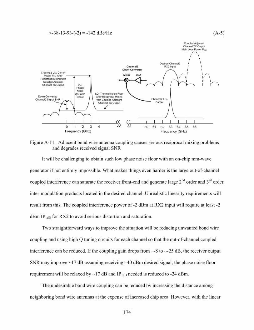
174
<-38-13-93-(-2) = -142 dBc/Hz (A-5)
Figure A-11. Adjacent bond wire antenna coupling causes serious reciprocal mixing problems and degrades received signal SNR
It will be challenging to obtain such low phase noise floor with an on-chip mm-wave
generator if not entirely impossible. What makes things even harder is the large out-of-channel
coupled interference can saturate the receiver front-end and generate large 2nd order and 3rd order
inter-modulation products located in the desired channel. Unrealistic linearity requirements will
result from this. The coupled interference power of -2 dBm at RX2 input will require at least -2
dBm IP1dB for RX2 to avoid serious distortion and saturation.
Two straightforward ways to improve the situation will be reducing unwanted bond wire
coupling and using high Q tuning circuits for each channel so that the out-of-channel coupled
interference can be reduced. If the coupling gain drops from ~-8 to ~-25 dB, the receiver output
SNR may improve ~17 dB assuming receiving –40 dBm desired signal, the phase noise floor
requirement will be relaxed by ~17 dB and IP1dB needed is reduced to -24 dBm.
The undesirable bond wire coupling can be reduced by increasing the distance among
neighboring bond wire antennas at the expense of increased chip area. However, with the linear

175
dimension of modern VLSI chip reaching ~cm range, it is possible to separate the bond-wire
antennas further than the 300 m assumed in previous discussion. The coupling can also be
reduced by increasing the resonant frequency separations among bond wire antennas and
Figure A-12. Alternative wireless FDMA interconnect architecture increases hardware sharing
and mitigates undesirable bond wire antenna coupling utilizing the bandpass filtering response of
mm-wave TX/RX front-ends to attenuate unwanted signals. To obtain maximal hardware
sharing, an alternate TDD interconnect circuit system shown in Figure A-12 could be utilized.
Only one PA and one LNA are needed for the three pairs of TX and RX, and only one bond wire
antenna is required on each side. This reduces the total number of antennas and also allows the
spacings among antennas to be increased. Thus, the mutual coupling among nearby bond wire
antennas in the architecture of Figure A-9 can be reduced. Nevertheless, this system can only be
used for the case where the three I/O data paths provided by the three wireless FDMA channels

176
are synchronized in terms of transmission and reception. The PA at mm-wave frequencies may
have difficulty of supporting linearity and output power for the three channels at the same time.
Three individual PA for each channel may have to be built and combined at the outputs.
One key component for TDD scheme is the mm-wave T/R switch. So far, it is assumed an
ideal component in the above discussions. At this point, according to mm-wave T/R switch
works done in our group using the TI CMOS process, ~60-70 GHz T/R switches have ~4 dB
insertion loss (IL) and ~20 dB isolation. The IL is going to dissipate a large portion of PA output
power and increase RX NF. This moderate performance of T/R switch is a serious concern for
the system in Figure A-12.
A.9 Alternate Architecture with Frequency Division Duplex Scheme
Alternate system architecture based on FDD scheme and the associated radio circuit
architecture for the wireless interconnects is also possible (Figure A-13).
The system does not need the non-ideal mm-wave T/R switch. The bidirectional
communication in the system is supported using two different frequency bands. On one side, 60
GHz band (low band) as reception and 80 GHz band (high band) for transmission. On the other
side, the use of the frequency bands is reversed. For the radio circuit system architecture, PA and
LNA can still be shared by three TX’s/RX’s. Unlike the TDD scheme in Figure A-12, real-time
bidirectional communication for three independent I/O data paths is possible with this
architecture. Constructing bond wire antenna that covers both the low and high bands with more
than 16-GHz bandwidth seems to be challenging. A high quality factor duplexer filter at mm-
wave is also a challenge. So instead of sharing one antenna, two bond wire antennas can be
shared by the three TX’s and the three corresponding RX’s respectively. If the PA cannot be
shared by the three channels because of its performance limits, then each TX will have to use its
own PA and antenna. An antenna and an LNA in RX however can still be shared. All the TX’s

177
and their antennas on one chip can be tuned to a different band from RX’s. Hence the
interference problem through bond wire antennas can be alleviated. Such an FDD scheme needs
Figure A-13. Wireless FDMA interconnect system using an FDD scheme utilizes two frequency bands for bidirectional communication, removes the T/R switch and reduces undesirable bond wire antenna coupling.
more bond wire antennas and occupies two frequency bands instead of one compared to the TDD
scheme shown in Figure A-12. Fortunately, adding bond wires should be straightforward, while
the frequency spectrum within the package (shielded) is ample to allow the usage of two bands.
The on-chip carrier generation scheme can be modified to provide carriers for two separate bands
by adding multiple buffers, offset mixers and notch filters (Figure A-14) to the synthesizer
architecture shown in Figure A-8 (B). Three LO signals at 78, 81 and 84 GHz (80 GHz band)
will be generated. The 80 GHz band will have ~18 GHz difference from the original 60 GHz

178
band consisting of 60, 63 and 66 GHz carrier frequencies. Inferred from the bond wire antenna
coupling study that two antennas resonant 6 GHz apart could have a coupling gain of ~ –16 dB,
the coupling gain between two bond wire antennas resonant at 18 GHz away (300 m apart)
could be as low as ~-25 dB. Combining with the frequency tuning response of active circuits
following the antenna, the isolation between the TX’s and RX’s could be higher than 40 dB. This
high isolation should alleviate all the issues facing TDD schemes described in the last section.
Table A-5 shows the system specification reflecting the adaptation of FDD scheme.
Figure A-14. Multiple buffers, notch filters and offset mixers can be added to the 60-GHz band frequency synthesizer in Figure A-8 (B) to generate the 80-GHz band LO signals needed by the FDD scheme

179
Table A-5. Wireless inter-chip interconnect system specification reflecting the adaptation of FDD scheme
Features Specifications
Data I/O path # 3
Multiple access FDMA
FDMA channel # 3
Data rate/ channel (Gbps) 1
Modulation DPSK
Duplex FDD
RF BW/ channel (GHz) 2
Channel spacing (GHz) 3
Channel freq (GHz) 60,63,66,78,81,84
Bit error rate 10-16
SNR required (dB) 13.5
Total data rate (Gbps) 3
A.10 Summary
In this chapter, a wireless interconnect system is proposed, targeting to alleviate the
package and interconnect problems for future large scale computing circuits. First, the package
and traditional wire interconnect challenges facing the digital circuits with increasingly higher
speed and higher integration are presented. These challenges motivate multiple potential
solutions and wireless interconnect is the one more compatible with mainstream CMOS
technology and bringing lower cost. To evaluate the feasibility of wireless interconnects in
digital bulk CMOS, a mm-wave band FDMA interconnect system in a multi-chip module is
proposed and studied. The system architecture, specification, and modulation scheme are
discussed, and the EM propagation channel and radiation structures are introduced. Specifically,
based on bond wire antennas measured characteristics, the interconnect link margin is estimated.
Following this, direct-conversion radio circuit architecture for the interconnect system is

180
examined and the considerations for a multiple output frequency synthesizer architecture design
are discussed. The system duplex scheme in the context of the direct-conversion architecture is
re-examined. It is found that the system based on TDD scheme could perform poorly due to non-
ideal performances of mm-wave T/R switches and undesirable coupling among bond wire
antennas. Hence an alternate architecture using FDD scheme is proposed to mitigate these issues.
The study in this chapter intends to identify general directions and potential issues of
designing a wireless interconnect system. More detailed works in system simulation and circuit
design are needed towards the realization of such a system.

181
LIST OF REFERENCES
[1] Institute of Electrical and Electronics Engineers, IEEE WLAN Standard, Piscataway, NJ: IEEE, 2008.
[2] Institute of Electrical and Electronics Engineers, IEEE WPAN Standard, Piscataway, NJ: IEEE, 2008.
[3] Institute of Electrical and Electronics Engineers, IEEE WBAN Standard, Piscataway, NJ: IEEE, 2008.
[4] G.E. Moore, “Cramming more components onto integrated circuits,” Electronics, vol. 38, no. 8, pp. 114-117, Apr. 1965.
[5] Semiconductor Industry Association, ©2007 ITRS, Int. Technol. Roadmap For Semiconductors, 2007 Edition, System Drivers, San Jose, CA: SIA, 2009.
[6] K. X. Zhang, “The challenges and opportunities in GHz microprocessor design on 0.13 m and beyond technologies,” in Proc. of 6th Int. Conf. on Solid-State and Integrated-Circuit Tech., Oct. 2001, pp. 1102-1106.
[7] J.-H. Park, “8 Gb MLC (multi-level cell) NAND flash memory using 63 nm process technology,” in IEEE IEDM Tech. Dig., Dec. 2004, pp 873- 876.
[8] V. Balan, “A 4.8–6.4-Gb/s Serial Link for Backplane Applications Using Decision Feedback Equalization,” IEEE J. Solid-State Circuits, vol. 40, no. 9, pp 1957-1967, Sep. 2005.
[9] R. B. Staszewski, “A 24mm2 Quad-Band Single-Chip GSM Radio with Transmitter Calibration in 90nm Digital CMOS,” in IEEE ISSCC Tech. Dig., Feb. 2008, pp 208-300.
[10] D. Seippel, M. Hammes, A. Hanke, and J. Kissing, “GSM/GPRS Single-Chip in 130nm CMOS: Challenges on RF for SoC Integration,” in IEEE RFIC Symp. Tech. Dig., Jun., 2006, pp. 4-180.
[11] M.-C. F. Chang, “Impact of CMOS Scaling on RF/Mixed-Signal Circuit Designs,” in Proc. of 8th Int. Conf. on Solid-State and Integrated Circuit Tech., May 2006, pp. 200-204.
[12] R. B. Staszewski, K. Muhammad and D. Leipold , “Digital RF Processor Techniques for Single-Chip Radios (Invited),” in IEEE CICC Tech. Dig., Sep. 2006, pp 789-796.
[13] J. Mitola, “The Software Radio Architecture,” IEEE Comm. Magazine, vol. 33, no. 5, pp. 26-38, May 1995.

182
[14] M. Feng, “Device Technologies for RF Front-End Circuits in Next-Generation Wireless Communications,” Proc of IEEE, vol. 92, no. 2, pp 354-375, Feb. 2004.
[15] H. S. Bennett, “Device and Technology Evolution for Si-Based RF Integrated Circuits,” IEEE Trans. Electron Dev., vol. 52, no. 7, pp. 1009-1019, Jul. 2005
[16] S. K. Yong and C.-C. Chong, “An Overview of Multigigabit Wireless through Millimeter Wave: Technology: Potentials and Technical Challenges,” EURASIP J. Wireless Comm. Networking, vol. 2007, pp 101-121, Dec. 2007.
[17] T. Cutler, “Unlicensed Wireless Data Communications,” Compliance Engineering Magazine, pp. 12-16, Jan. 2002.
[18] D. Cabric, M. S.W. Chen, D. A. Sobel, S. Wang, J. Yang, and R. W. Brodersen, ”Novel Radio Architectures for UWB, 60 GHz, and Cognitive Wireless Systems,” EURASIP J. Wireless Comm. Networking, vol. 2006, pp. 21-41, Dec. 2007.
[19] System Support Solutions Inc., BridgeWave 60-GHz Products Brochure, Orono, MN: SSS, 2008.
[20] N. Guo, R. C. Qiu, S. S. Mo, and K. Takahashi, “60-GHz Millimeter-Wave Radio: Principle, Technology, and New Results,” EURASIP J. Wireless Comm. Networking, vol. 2007, pp. 51-81, Dec. 2007.
[21] P. Smulders, “Exploiting the 60 GHz Band for Local Wireless Multimedia Access: Prospects and Future Directions,” IEEE Comm. Magazine, vol. 33, no. 5, pp. 140-147, Jan, 2002.
[22] J. W, Meyer, Millimeter Wave Research: Past, Present and Future, Lincoln Laboratory Technical Report 389, Boston, MA: MIT, May 1965.
[23] A. Hajimiri, “mm-Wave Silicon ICs: Challenges and Opportunities,” in IEEE CICC Tech. Dig., Sep. 2007, pp. 741-747.
[24] R. A. Pucel, “Design Considerations for Monolithic Microwave Circuits,” IEEE Trans. Microw. Theory Tech., vol. 29, no. 6, pp 513-534, Jun. 1981.
[25] D. Yu, “Ultra High-Speed 0.25-μm Emitter InP-InGaAs SHBTs with fmax of 687 GHz,” in IEEE IEDM Tech. Dig., Dec.,2004, pp. 557-560.
[26] K. Ohata, “1.25Gbps Wireless Gigabit Ethernet Link at 60 GHz-Band,” in IEEE IMS Tech. Dig., Jun. 2003, pp. 373-376.
[27] H. Zirath, C. Fager, M. Garcia, P. Sakalas, L. Landen, and A. Alping, “Analog MMICs for Millimeter-Wave Applications Based on a Commercial 0.14-m pHEMT Technology”, IEEE Trans. Microw. Theory Tech., vol. 49, no. 11, pp. 1312-1322, Nov. 2001

183
[28] S. E. Gunnarsson, “Highly Integrated 60 GHz Transmitter and Receiver MMICs in a GaAs pHEMT Technology”, IEEE J. Solid-State Circuits, vol. 40, no. 11, pp 2174-2186, Nov. 2005.
[29] E. Laskin, “170-GHz Transceiver with On-Chip Antennas in SiGe Technology,” in IEEE RFIC Symp. Tech. Dig., Jun. 2008, pp. 637-640.
[30] S. T. Nicolson, “A 1.2V, 140GHz receiver with on-die antenna in 65nm CMOS”, in IEEE RFIC Symp. Tech. Dig., Jun. 2008, pp 229-232.
[31] J. S. Kilby, “Miniaturized Electronic Circuits,” United States Patent 3138743, issued on Jun. 23, 1964.
[32] J. S. Kilby, “Method of Making Miniaturized Electronic Circuits,” United States Patent 3261081, issued on Jul. 19, 1966.
[33] R. N. Noyce, "Microelectronics," Scientific American, vol. 237, no. 3, pp. 62-69, Sep. 1977.
[34] E. Laskin and S. Voinigescu, “Towards 100+ GHz Electronics”, in CMOSET Tech. Dig., Sep., 2007, pp 150-153.
[35] B. Gaucher, “Progress in SiGe Technology Toward Fully Integrated mmWave Ics,” in IEEE ISTDM Tech. Dig., Oct. 2006, pp. 1-2.
[36] B. Floyd, S. Reynolds, U. Pfeiffer, T. Zwick, T. Beukema, and B. Gaucher, “SiGe Bipolar Transceiver Circuits Operating at 60GHz,” IEEE J. Solid-State Circuits, vol. 40, no. 1, pp. 156-167, Jan. 2005.
[37] A Babakhani, X Guan, A Komijani, A Natarajan, and A. Hajimiri, “A 77-GHz Phased-Array Transceiver with On-Chip antennas in silicon: Receiver and Antennas,” IEEE J. Solid-State Circuits, vol. 41, no. 12, pp. 2795-2806, Dec. 2006.
[38] S. Reynolds, “Second Generation 60-GHz Transceiver Chipset Supporting Multiple Modulations at Gb/s data rates (Invited),” in IEEE BCTM Tech. Dig., Sep. 2007, pp. 192-197.
[39] J. Pekarik, ‘‘RF CMOS Technology from 0.25 m to 65 nm: The State of the Art,’’ in IEEE CICC Tech. Dig., Sep. 2004, pp. 217-224.
[40] C. H. Doan, “Millimeter-wave CMOS design,” IEEE J. Solid-State Circuits, vol. 40, no. 3, pp. 144 -155, Jun. 2005.
[41] T. Yao, “60-GHz PA and LNA in 90-nm RF-CMOS,” in IEEE RFIC Symp. Tech. Dig., Jun., 2006, pp. 100-103.

184
[42] S. Emami, C.H. Doan, A.M. Niknejad, R. W. Brodersen, “A 60-GHz Down-Converting CMOS Single-gate Mixer”, in RFIC Symp. Tech. Dig., June, 2005, pp. 163-166.
[43] B. Razavi, “CMOS Transceivers for the 60-GHz Band,” in IEEE RFIC Symp. Tech. Dig., Jun., 2006, pp. 106-109.
[44] Semiconductor Industry Association, Int. Technol. Roadmap For Semiconductors, 2005 Edition, Radio Frequency And Analog/Mixed-Signal Technologies For Wireless Communications, San Jose, CA: SIA, 2005.
[45] S. E. Thompson, “A 90-nm Logic Technology Featuring Strained-Silicon,” IEEE Trans. Electron Dev., vol.51, no. 3, pp.1790-1797, May 2004.
[46] T. O. Dickson, “The Invariance of Characteristic Current Densities in Nanoscale MOSFETs and Its Impact on Algorithmic Design Methodologies and Design Porting of Si(Ge) (Bi)CMOS High-Speed Building Blocks,“ IEEE J. Solid-State Circuits, vol. 41, no. 8, pp. 1006-1016, Aug. 2006.
[47] R. Dennard, “Design of ion-implanted MOSFETs with very small physical dimensions,” IEEE J. Solid-State Circuits, vol. 9, no. 5, pp. 256-268, Oct. 1974.
[48] Y. Taur and T. H. Ning, Modern VLSI Devices, New York, NY: Cambridge University Press, 1998.
[49] L. M. Franca-Neto, “Fully Integrated CMOS Radios from RF to Millimeter Wave Frequencies,” Intel Tech. J., vol 08, issue 03, pp. 1-10, Aug. 2004.
[50] BSIM Group, BSIM 4.3.0 MOSFET Model-User’s Manual, Berkeley, CA: University of California, 2003.
[51] S. F. Tin, A. A. Osman, K. Mayaram, and C. Hu, “A Simple Subcircuit Extension of the BSIM3v3 Model for CMOS RF Design,” IEEE J. Solid-State Circuits, vol. 35, no. 4, pp.612-624, Apr. 2000.
[52] C. H. Doan, S. Emami, A. M. Niknejad, and R. W. Brodersen, “Millimeter-Wave CMOS Device Modeling And Simulation,” in IEEE ISCAS Tech. Dig., May. 2004, pp. 524-527.
[53] C. H. Doan, S. Emami, A. M. Niknejad, and R. W. Brodersen, “Design of CMOS for 60 GHz applications,” in IEEE ISSCC Tech. Dig., Feb. 2004, pp. 440-538.
[54] M. W. Pospieszalski, “On the measurement of noise parameters of microwave two-ports,” in IEEE IMS Tech. Dig., Apr. 1986, pp.456-458.
[55] C. H. Doan, S. Emami, A. M. Niknejad, and R. W. Brodersen, “Millimeter-Wave CMOS Design,” IEEE J. Solid-State Circuits, vol. 40, no. 1, pp. 144-155, Jan. 2005.

185
[56] C. Enz, and Y. Cheng, “MOS Transistor Modeling for RF IC Design,” IEEE Trans. Solid-State Circuits, vol.35, no.2, pp 186-123, Feb. 2000.
[57] S.-M. Yim, “ COMPONENTS AND CIRCUIT ANALYSIS TECHNIQUES FOR A MULTI-BAND WIRELESS RECEIVER”, PhD Thesis, UNIVERSITY OF FLORIDA, Gainesville, FL, 2003.
[58] T. H. Lee, The Design of CMOS Radio-Frequency Integrated Circuits, New York, NY: Cambridge University Press, 1998.
[59] Ansoft LLC., HFSS User Guide, Version 10.0, Pittsburgh, PA: Ansoft LLC., 2005.
[60] C-M. Hung, Y.-C. Ho, I.-C. Wu, and K. K. O, “High-Q capacitors implemented in a CMOS low-power wireless applications,” IEEE Trans. Microw. Theory Tech., vol. 46, no. 5, pp. 505–511, May 1998.
[61] N. Zhang and K. K. O, “ 94 GHz Voltage Controlled Oscillator with 5.8 % Tuning Range in Bulk CMOS,” IEEE Microw. Wireless Compon. Lett., vol. 15, no. 8, pp.493-495, Aug. 2008.
[62] C. P. Yue and S. S. Wong, “On-Chip Spiral Inductors with Patterned Ground Shields for Si-Based RF IC’s,” IEEE J. Solid-State Circuits, vol. 33, no. 5, pp. 743-752, May 1998.
[63] FastHenry Group, FastHenry User’s Guide, Version 3.0, Boston, MA: MIT, 1996.
[64] K. K. O, “Wireless Communication Using Integrated Antennas,” in Proc. Int. Interconnect Technol.. Conf., Jun. 2003, pp.111-113.
[65] B. A. Floyd, “A CMOS WIRELESS INTERCONNECT SYSTEM FOR MULTI-GIGAHERTZ CLOCK DISTRIBUTION,” Ph.D. Thesis, UNIVERSITY OF FLORIDA, Gainesville, FL, May 2001.
[66] U. R. Pfeiffer, “Low-loss Contact Pad with Tuned Impedance for Operation at Millimeter Wave Frequencies,” in SPI Tech. Dig., May 2005, pp 61-64.
[67] G. Gonzalez, Microwave Transistor Amplifier: Analysis and Design, 2nd edition, New York, NY, Pearson Print on Demand, 1996.
[68] D. K. Shaeffer and T. H. Lee, “A 1.5-V, 1.5-GHz CMOS low noise amplifier,” IEEE J. Solid-State Circuits, vol. 32, no.5, pp. 745-759, May. 1997.
[69] Y.-C. Ho, M. Biyani, J. Colvin, C. Smithhisler, and K. K. O, “A 3-V Low Noise Amplifier Implemented Using a 0.8-m CMOS Process with Three Metal Layers for 900 MHz Operation,” IEE Electronics Lett., vol. 32, no. 13, pp. 1191-1193, Jun. 1996.

186
[70] C. H. Doan, S. Emami, A. M. Niknejad, and R. W. Brodersen, “Design of CMOS for 60 GHz applications,” in IEEE ISSCC Tech. Dig., Feb. 2004, pp. 440–441.
[71] C.-M. Lo, C.-S. Lin, and H. Wang, “A Miniature V-band 3-Stage Cascode LNA in 0.13µm CMOS,” in IEEE ISSCC Tech. Dig., Feb. 2006, pp 1254-1255.
[72] S. Emami, C.H. Doan, A.M. Niknejad and R.W. Brodersen, “A highly integrated 60 GHz CMOS front-end receiver,” in IEEE ISSCC Tech. Dig., Feb. 2007, pp. 190–191.
[73] T. Mitomo, R. Fujimoto, N. Ono, R. Tachibana, H. Hoshino, Y. Yoshihara, Y. Tsutsumi, and I. Seto, “A 60-GHz CMOS Receiver Front-End With Frequency Synthesizer,” IEEE J. Solid-State Circuits, vol. 43, no. 4, pp. 1030–1037, April 2008.
[74] K.-H. Chen, C. Lee and S.-I. Liu, “A Dual-band 61.4~63GHz/75.5~77.5GHz CMOS Receiver in a 90nm Technology,” in VLSI Symp. on Circuits Tech. Dig., June 2008, pp. 160–161.
[75] M. Khanpour, K. W. Tang, P. Garcia, and S. P. Voinigescu, “A Wideband W-Band Receiver Front-End in 65-nm CMOS,” IEEE J. Solid-State Circuits, vol. 43, no. 8, pp. 1717–1730, Aug. 2008.
[76] E. Laskin, M. Khanpour, R. Aroca, K.W. Tang, P. Garcia, and S. P. Voinigescu, “ A 95GHz receiver with fundamental-frequency VCO and static frequency divider in 65nm digital CMOS, ” in IEEE ISSCC Tech. Dig, Feb. 2008, pp. 180–605.
[77] N. Zhang, C.-M. Hung, and K. K. O, “80-GHz Tuned Amplifier in Bulk CMOS,” IEEE Microw. Wireless Compon Lett., vol.18, no.2, pp. 121-123, Feb. 2008.
[78] B. A. Floyd, J. Mehta, C. Gamero, and K. K. O, “ A 900-MHz, 0.8-m CMOS low noise amplifier with 1.2-dB noise figure,” in IEEE CICC Tech. Dig., May, 1999, pp. 661-664.
[79] Jri Lee, “High-Speed Circuit Designs for Transmitters in Broadband Data Links,” IEEE J. Solid-State Circuits, vol. 41, no. 5, pp 1004-1015, May 2006.
[80] B. Razavi, RF Microelectronics, Pearson Education Asia Limited, 2003, pp. 212.
[81] F. Y. Yuan, “Electromagnetic Modeling and Signal Integrity Simulation of Power/Ground Networks in High Speed Digital Packages and Printed Circuit Boards,” in DAC Tech. Dig. , Jun. 1998, pp. 300–303.
[82] T. Blalack, J. Lau, F. J. R. Clement, and B. A. Wooley, “Experimental results and modeling of noise coupling in a lightly doped substrate,” in IEEE IEDM Tech. Dig., Dec. 1996, pp. 623–626.
[83] A. Samavedam, A. Sadate, K. Mayaram, and T. S. Fiez, “A scalable substrate noise coupling model for design of mixed-signal IC’s,” IEEE J. Solid-State Circuits, vol. 35, no. 6, pp. 895–904, Jun. 2000.

187
[84] T. Blalack, Y. Leclercq, and C.P. Yue, “On-Chip RF Isolation Techniques,” in IEEE BCTM Tech. Dig., Oct. 2002, pp. 205–211.
[85] Agilent Inc., Agilent PNA E8361A Manual, Santa Clara, CA: Agilent Inc., 2008.
[86] Z. Shen, “Advanced Microwave/Millimeter-Wave Imaging Technology,” J. Plasma Fusion Research, vol. 2, pp. 1019-1023, May 2007.
[87] L. M. Franca-Neto, R. Bishop, and B. Bloechel, “64 GHz and 100 GHz VCOs in 90 nm Using Optimum Pumping Method,” in IEEE ISSCC Tech. Dig., Feb.2004, pp. 444-445.
[88] C. Cao and K.K.O, “A 90-GHz voltage-controlled oscillator with a 2.2-GHz tuning range in 130-nm CMOS technology,” in Symp. VLSI Circuits Tech. Dig., Jun. 2005, pp. 242–243.
[89] C. Cao and K.K.O, “ Millimeter-Wave Voltage-Controlled Oscillators in 0.13 m CMOS Technology,” IEEE J. Solid-State Circuits, vol. 41, no. 6, pp 1297-1304, Jun. 2006.
[90] C. Cao and K.K.O, “A 140-GHz Fundamental Mode Voltage-Controlled Oscillator in 90-nm CMOS Technology,” IEEE Microw. Wireless Compon. Lett., vol. 16, no. 10, pp 555-557, Oct. 2006.
[91] Z.-M. Tsai; C.-S. Lin; Huang, C.F. Chern, and H. Wang, “A Fundamental 90-GHz CMOS VCO Using New Ring-Coupled Quad,” IEEE Microw. Wireless Compon. Lett., vol. 17, no. 3, pp 226-228, Mar. 2007,
[92] P.-C. Huang, M.-D. Tsai, H. Wang, C.-H. Chen, and C.-S. Chang, “A 114 GHz VCO in 0.13 m CMOS technology,” in IEEE ISSCC Tech. Dig., Feb.2005, pp. 404-405.
[93] P. C. Huang, R.-C. Liu, H.-Y. Chang, C.-S. Lin, M.-F. Lei, H. Wang, C.-Y. Su, and C.-L. Chang, “A 131 GHz push-push VCO in 90-nm CMOS technology,” in IEEE RFIC Symp. Tech. Dig., Jun. 2005, pp 613–616.
[94] C. Cao, E. Seok and K.K.O, “ 192 GHz push-push VCO in 0.13 m CMOS,” IEE Electronics Lett., vol. 42, no.4, pp 208-210, Feb 2006.
[95] K. Ishibashi, M. Motoyoshi, N. Kobayashi, and M. Fujishima “76 GHz CMOS Voltage-Controlled Oscillator with 7% Frequency Tuning Range,” in Symp. VLSI Circuits Tech. Dig., Jun. 2007, pp. 176–177.
[96] C, Lam, “Phase-locked loop with self-selecting multi-band VCO,” United States Patent 6806786, issued on Oct. 19, 2004.
[97] J. J. Hung, T. M. Hancock, and G.M. Rebeiz, “A 77 GHz SiGe Sub-Harmonic Balanced Mixer,” IEEE J. Solid-State Circuits, vol. 49, no.11, pp. 2167-2173, Nov. 2005.
188
[98] R. M. Kodkani and L.E. Larson, “An Integrated 50-GHz SiGe Sub-Harmonic Mixer/Downconverter with a Quadrature Ring VCO,” in IEEE Topical Meeting Si. Mono. Integr. Circuits in RF Systems Dig., , Jan. 2007, pp 223-226.
[99] J. -H. Tsai and T. -W. Huang, “35-65-GHz CMOS Broadband Modulator and Demodulator with Sub-harmonic Pumping for MMW Wireless Gigabit Applications,” IEEE Trans. Microw. Theory Tech., vol. 55, no. 10, pp.2075-2085, Oct, 2007.
[100] N. Zhang, H. Xu, H.-T. Wu, and K. K. O, “W-band Active Down-Conversion Mixer in Bulk CMOS,” IEEE Microw. Wireless Compon Lett., vol. 19, no. 2, pp. 98-100, Feb. 2009.
[101] Maxim Integrated Products Inc., “Three Methods of Noise Measurement,” Application Note 2875, Dallas, TX, Nov. 21, 2003.
[102] B. M. Motlagh S. E. Gunnarsson, M. Ferndanl, and H. Zirath, “Fully Integrated 60-GHz Single-ended Resistive Mixer in 90-nm CMOS Technology,” IEEE Microw. Wireless Compon. Lett., vol.16, no.1, pp 25-27, Jan. 2006.
[103] C.-S Lin, P.-S Wu, H.-Y Chang, and H. Wang, “A 9-50-GHz Gilbert-cell Down-conversion Mixer in 0.13-m CMOS Technology,” IEEE Microw Wireless Compon. Lett., vol.16, no.5, pp 293-295, May. 2006.
[104] M. Varonen, M. Karkkainen, and K. Halonen, “V-band Balanced Resistive Mixer in 65-nm CMOS,” in Europe. Solid-State Circ. Conf. Tech. Dig., Sep, 2007, pp 360-363.
[105] Institute of Electrical and Electronics Engineers, Virtual Museum Radar Introduction, Piscataway, NJ: IEEE, 2008.
[106] H. Rohling, “Research Activities In Automotive Radar,” in Symp. MSMW Tech. Dig., Jun., 2001, pp. 155-158.
[107] K.M. Strohm, H.-L. Bloecher, R. Schneider, and J. Wenger, “Development of future short range radar technology,” in Proc. Europe. Radar Conf., Oct. 2005, pp. 165-168.
[108] Directorate General Information Society, “A 2nd Generation Forward Looking Radar Sensor News for Adaptive Cruise Control,” The Directorate C Lett. Mini. Embed. Systems App., vol.2, no.4, pp 2, May 2004.
[109] W. L. Stutzman and G. A. Thiele, Antenna Theory and Design, 2nd Edition, New York, NY: Wiley, 1998.
[110] X. Li, T. Brogan, M. Esposito, B. Myers and K. K. O, “ A Comparison of CMOS and SiGe LNA’s and Mixers for Wireless LAN Application,” in IEEE CICC Tech. Dig., May, 2001, pp. 531-534.

189
[111] Y. Deguchi, K. Sakakibara, N. Kikuma, and H. Hirayama, “Millimeter-wave microstrip-to-waveguide transition operating over broad frequency bandwidth,” in IEEE IMS Tech. Dig., Jun. 2005, pp. 2107-2110.
[112] C. Cao, Y. Ding, and K. K. O, “A 50-GHz Phase-Locked Loop in 0.13-m CMOS,” IEEE J. Solid-State Circuits, vol. 42, no. 8, pp 1649-1656, Aug. 2007.
[113] C. Cao and K. K. O, “A Power Efficient 26-GHz 32:1 Static Frequency Divider in 130-nm Bulk CMOS”, IEEE Microw Wireless Compon. Lett., vol. 15, no. 11, pp 233-235, Nov. 2005.
[114] R. Mohanavelu and P. Heydari, “A Novel 40-GHz Flip-Flop-Based Frequency Divider in 0.18 mm CMOS,” in Proc. of ESSCIRC, Sep. 2005, pp. 185-188.
[115] Yanping Ding, “CMOS SYNTHESIZERS FOR 24-GHZ RADIO,” Ph.D. Thesis, UNIVERSITY OF FLORIDA, Gainesville, FL, 2007.
[116] C. Cao, “A 24-GHz FULLY-INTEGRATED CMOS TRANSMITTER WITH ON-CHIP ANTENNA,” Ph.D. Thesis, UNIVERSITY OF FLORIDA, Gainesville, FL, 2006.
[117] C. Lee and S.I. Liu, “A 58-to-60.4GHz Frequency Synthesizer in 90nm CMOS,” in IEEE ISSCC Tech. Dig., Feb. 2007, pp. 196-197.
[118] H. Hoshino et al., “A 60-GHz Phase-Locked Loop with Inductor-less Prescaler in 90-nm CMOS,” in Proc. of ESSCIRC, pp. 472-475, Sep. 2007.
[119] J. Lee, M. Liu and H. Wang, “A 75-GHz Phase-Locked Loop in 90-nm CMOS Technology,” IEEE J. Solid-State Circuits, vol. 43, no. 6, pp. 1414-1426, June 2008.
[120] K.-H. Tsai and Shen-Iuan Liu, “A 43.7mW 96GHz PLL in 65nm CMOS,”, in IEEE ISSCC Tech. Dig., Feb. 2009, pp. 276-277.
[121] K. Scheir, G. Vandersteen, Y. Rolain, and P. Wambacq, “A 57-to-66GHz Quadrature PLL in 45nm Digital CMOS,” in IEEE ISSCC Tech. Dig., Feb. 2009, pp. 494-495.
[122] Vipul Jain, Fred Tzeng, Lei Zhou and Payam Heydari, “A Single-Chip Dual-Band 22-to-29GHz/77-to-81GHz BiCMOS Transceiver for Automotive Radars,” in IEEE ISSCC Tech. Dig., Feb. 2009, pp. 308-309.
[123] Yoichi Kawano et al, “A 77GHz Transceiver in 90nm CMOS,” in IEEE ISSCC Tech. Dig., Feb. 2009, pp. 310-311.
[124] K. K. O, “Wireless Inter-chip Interconnect System,” Proposal to NSF, UNIVERSITY OF FLORIDA, Gainesville, FL, 2004.
[125] H. K. Kwon, “SIP solution for high-end multimedia cellular phone,” in IEEE IMAPS Tech. Dig., Sep. 2003, pp.165-169.

190
[126] T. Oka, “System-In-a-Package Stacked Flash Memory and Logic LSI,” in Semicon Japan, 2000.
[127] N. Miura, “An 11Gb/s Inductive-Coupling Link with Burst Transmission,” in IEEE ISSCC Tech. Dig., Feb. 2008, pp 298-614.
[128] A. V. Krishnamoorthy, “Optical interconnects for commodity silicon technologies,” in IEEE Int. Conf. Innovative Systems In Silicon Tech. Dig., Oct 1997, pp 201-202.
[129] J. Ko, J. Kim, Z. Xu, Q. Gu, C. Chien, and M.F. Chang, “An RF/Baseband FDMA-Interconnect Transceiver for Reconfigurable Multiple Access Chip-to-Chip Communication,” in IEEE ISSCC Tech. Dig., Feb. 2005, pp 208-211.
[130] H.-T. Wu, M. Tekle, C.S. Nallani, N. Zhang and K. K. O, “Bond Wire Antennas for Operations Near 60 GHz,” IEEE Trans. Microwave Theo. Tech., Submitted.
[131] C. Sandner and A. Wiesbauer, “A 3 GHz to 7 GHz fast-hopping frequency synthesizer for UWB,” in Proc. Int. Ultra Wideband Syst. Workshop, 2004, pp. 405–409.
[132] D. Huang, “A 60GHz CMOS VCO Using On-Chip Resonator with Embedded Artificial Dielectric for Size, Loss and Noise Reduction,” in IEEE ISSCC Tech. Dig., Feb. 2006, pp 314-315.

BIOGRAPHICAL SKETCH
Ning Zhang received his B.S. degree from the Dept. of Electronics and Communication
Engineering, South China University of Technology, Guangzhou, China in 2001 and his M.S.
degree from the Dept. of Electrical and Computer Engineering, University of Wisconsin-
Madison in 2004 with research in THz micro-vacuum devices design. He received his Ph.D.
degree from the Dept. of Electrical and Computer Engineering, University of Florida in August
2009, focusing on CMOS millimeter-wave/RF circuits and systems and their applications. He
worked on inductor extraction, circuit simulators benchmarking, and power amplifier package
modeling as an intern in Wireless Branch of Conexant Inc. Melbourne, Florida in 2007.


